CN116015022A - Drive circuit and related control chip circuit, power adapter and electronic equipment - Google Patents
Drive circuit and related control chip circuit, power adapter and electronic equipment Download PDFInfo
- Publication number
- CN116015022A CN116015022A CN202210109729.7A CN202210109729A CN116015022A CN 116015022 A CN116015022 A CN 116015022A CN 202210109729 A CN202210109729 A CN 202210109729A CN 116015022 A CN116015022 A CN 116015022A
- Authority
- CN
- China
- Prior art keywords
- circuit
- resistor
- tube
- nmos tube
- nmos
- Prior art date
- Legal status (The legal status is an assumption and is not a legal conclusion. Google has not performed a legal analysis and makes no representation as to the accuracy of the status listed.)
- Granted
Links
Images




Classifications
-
- H—ELECTRICITY
- H02—GENERATION; CONVERSION OR DISTRIBUTION OF ELECTRIC POWER
- H02M—APPARATUS FOR CONVERSION BETWEEN AC AND AC, BETWEEN AC AND DC, OR BETWEEN DC AND DC, AND FOR USE WITH MAINS OR SIMILAR POWER SUPPLY SYSTEMS; CONVERSION OF DC OR AC INPUT POWER INTO SURGE OUTPUT POWER; CONTROL OR REGULATION THEREOF
- H02M1/00—Details of apparatus for conversion
- H02M1/08—Circuits specially adapted for the generation of control voltages for semiconductor devices incorporated in static converters
-
- H—ELECTRICITY
- H02—GENERATION; CONVERSION OR DISTRIBUTION OF ELECTRIC POWER
- H02M—APPARATUS FOR CONVERSION BETWEEN AC AND AC, BETWEEN AC AND DC, OR BETWEEN DC AND DC, AND FOR USE WITH MAINS OR SIMILAR POWER SUPPLY SYSTEMS; CONVERSION OF DC OR AC INPUT POWER INTO SURGE OUTPUT POWER; CONTROL OR REGULATION THEREOF
- H02M1/00—Details of apparatus for conversion
- H02M1/44—Circuits or arrangements for compensating for electromagnetic interference in converters or inverters
-
- Y—GENERAL TAGGING OF NEW TECHNOLOGICAL DEVELOPMENTS; GENERAL TAGGING OF CROSS-SECTIONAL TECHNOLOGIES SPANNING OVER SEVERAL SECTIONS OF THE IPC; TECHNICAL SUBJECTS COVERED BY FORMER USPC CROSS-REFERENCE ART COLLECTIONS [XRACs] AND DIGESTS
- Y02—TECHNOLOGIES OR APPLICATIONS FOR MITIGATION OR ADAPTATION AGAINST CLIMATE CHANGE
- Y02B—CLIMATE CHANGE MITIGATION TECHNOLOGIES RELATED TO BUILDINGS, e.g. HOUSING, HOUSE APPLIANCES OR RELATED END-USER APPLICATIONS
- Y02B70/00—Technologies for an efficient end-user side electric power management and consumption
- Y02B70/10—Technologies improving the efficiency by using switched-mode power supplies [SMPS], i.e. efficient power electronics conversion e.g. power factor correction or reduction of losses in power supplies or efficient standby modes
Landscapes
- Engineering & Computer Science (AREA)
- Power Engineering (AREA)
- Physics & Mathematics (AREA)
- Electromagnetism (AREA)
- Electronic Switches (AREA)
Abstract
本申请提供了一种驱动电路和相关的控制芯片电路、电源适配器及电子设备,该驱动电路包括:运放电路、比较器、第一NMOS管、第二NMOS管、第三NMOS管、第一PMOS管、第二PMOS管、第一驱动控制模块、第二驱动控制模块,其中,所述第一电阻、所述第二电阻、所述第一NMOS管用于形成LDO负反馈系统。采用本申请实施例能够解决在充电应用中,由于GaN功率管导致的EMI问题和满足GaN功率管驱动电压的精度要求。

The present application provides a driving circuit, a related control chip circuit, a power adapter and electronic equipment, the driving circuit includes: an operational amplifier circuit, a comparator, a first NMOS transistor, a second NMOS transistor, a third NMOS transistor, a first A PMOS transistor, a second PMOS transistor, a first drive control module, and a second drive control module, wherein the first resistor, the second resistor, and the first NMOS transistor are used to form an LDO negative feedback system. The embodiment of the present application can solve the EMI problem caused by the GaN power tube in the charging application and satisfy the accuracy requirement of the driving voltage of the GaN power tube.
Description
技术领域technical field
本申请涉及电子技术领域,具体涉及一种驱动电路和相关的控制芯片电路、电源适配器及电子设备。The present application relates to the field of electronic technology, in particular to a drive circuit and related control chip circuits, power adapters and electronic equipment.
背景技术Background technique
随着工艺的进步和缺陷率的不断降低,氮化镓(GaN)在交直流电力转换、改变电压电平、并且以一定数量的函数确保可靠电力供应的电子电源中的优势越来越明显。With the advancement of technology and the continuous reduction of defect rate, the advantages of gallium nitride (GaN) in electronic power supplies for AC and DC power conversion, changing voltage levels, and ensuring reliable power supply with a certain number of functions are becoming more and more obvious.
进而,实际应用中,会考虑将GaN用于作为GaN功率管的材料,但是,在充电过程中,由于GaN工作在较高的频率,会存在较大的di/dt,进而会引起严重的电磁干扰(electromagnetic interference,EMI),因此,如何解决在充电应用中,由于GaN功率管导致的EMI问题亟待解决。Furthermore, in practical applications, GaN will be considered as the material of GaN power tubes. However, during the charging process, because GaN works at a higher frequency, there will be a large di/dt, which will cause serious electromagnetic waves. Electromagnetic interference (EMI), therefore, how to solve the EMI problem caused by the GaN power tube in the charging application needs to be solved urgently.
发明内容Contents of the invention
本申请实施例提供了一种驱动电路和相关的控制芯片电路、电源适配器及电子设备,能够解决在充电应用中,由于GaN功率管导致的EMI问题和满足GaN功率管驱动电压的精度要求。The embodiment of the present application provides a driving circuit, related control chip circuit, power adapter and electronic equipment, which can solve the EMI problem caused by the GaN power tube in the charging application and meet the accuracy requirement of the driving voltage of the GaN power tube.
第一方面,本申请实施例提供一种驱动电路,所述驱动电路包括:运放电路、比较器、第一NMOS管、第二NMOS管、第三NMOS管、第一PMOS管、第二PMOS管、第一驱动控制模块、第二驱动控制模块,其中,In the first aspect, the embodiment of the present application provides a driving circuit, the driving circuit includes: an operational amplifier circuit, a comparator, a first NMOS transistor, a second NMOS transistor, a third NMOS transistor, a first PMOS transistor, a second PMOS transistor tube, the first drive control module, and the second drive control module, wherein,
所述运放电路的同相输入端连接第一电源,所述运放电路的输出端连接所述第一NMOS管的第一端,所述第一NMOS管的第三端连接第二电源,所述第一MOS管的第二端连接第一电阻的一端,所述第一电阻的另一端连接所述运放电路的反相输入端以及通过第二电阻进行接地;The non-inverting input end of the operational amplifier circuit is connected to the first power supply, the output end of the operational amplifier circuit is connected to the first end of the first NMOS transistor, and the third end of the first NMOS transistor is connected to the second power supply, so The second end of the first MOS transistor is connected to one end of the first resistor, and the other end of the first resistor is connected to the inverting input end of the operational amplifier circuit and grounded through the second resistor;
所述比较器的同相输入端连接第三电源,所述比较器的输出端连接或门电路的第一输入端,所述或门电路的第二输入端用于接入驱动信号,所述驱动信号还被输入所述第一驱动控制模块的第一端;The non-inverting input terminal of the comparator is connected to the third power supply, the output terminal of the comparator is connected to the first input terminal of the OR gate circuit, the second input terminal of the OR gate circuit is used to access the driving signal, and the driving The signal is also input into the first end of the first drive control module;
所述或门电路的输出端连接所述第二驱动控制模块的第一端,所述第二驱动控制模块的第二端连接第二PMOS管的第一端;所述第二PMOS管的第二端连接所述第一PMOS管的第二端以及所述第二NMOS端的第二端,所述第二PMOS管的第三端连接驱动端口,所述驱动端口用于驱动GaN功率管;所述第二NMOS管的第三端还连接第三电阻的一端,第三电阻的另一端连接第四电阻的一端以及所述比较器的反相输入端;The output end of the OR gate circuit is connected to the first end of the second drive control module, and the second end of the second drive control module is connected to the first end of the second PMOS transistor; the first end of the second PMOS transistor The two ends are connected to the second end of the first PMOS transistor and the second end of the second NMOS end, the third end of the second PMOS transistor is connected to a driving port, and the driving port is used to drive a GaN power transistor; The third end of the second NMOS transistor is also connected to one end of the third resistor, and the other end of the third resistor is connected to one end of the fourth resistor and the inverting input end of the comparator;
所述第二NMOS管的第一端连接第五电阻的一端,所述第五电阻的另一端连接所述第一NMOS管的第一端以及通过第一电容进行接地;所述第二NMOS管的第三端连接所述第二电源;The first end of the second NMOS transistor is connected to one end of the fifth resistor, and the other end of the fifth resistor is connected to the first end of the first NMOS transistor and grounded through the first capacitor; the second NMOS transistor the third end of which is connected to the second power supply;
所述第一驱动控制模块的第二端连接所述第一PMOS管的第一端,所述第一驱动控制模块的第三端连接所述第三NMOS管的第一端以及所述第二驱动控制模块的第三端,所述第三NMOS管连接所述第二PMOS管的第三端,所述第三NMOS管的第二端接地。The second end of the first drive control module is connected to the first end of the first PMOS transistor, and the third end of the first drive control module is connected to the first end of the third NMOS transistor and the second end of the second NMOS transistor. The third end of the drive control module, the third NMOS transistor is connected to the third end of the second PMOS transistor, and the second end of the third NMOS transistor is grounded.
第二方面,本申请实施例提供一种控制芯片电路,所述控制芯片电路包括如上述第一方面所描述的驱动电路。In a second aspect, an embodiment of the present application provides a control chip circuit, and the control chip circuit includes the driving circuit as described in the first aspect above.
第三方面,本申请实施例提供一种电源适配器,所述电源适配器包括如第一方面所描述的驱动电路,或者,如第二方面所描述的控制芯片电路。In a third aspect, an embodiment of the present application provides a power adapter, the power adapter includes the drive circuit described in the first aspect, or the control chip circuit described in the second aspect.
第四方面,本申请实施例提供一种电子设备,所述电子设备包括如第一方面所描述的驱动电路,或者,如第二方面所描述的控制芯片电路,或者,如第三方面所描述的电源适配器。In the fourth aspect, the embodiment of the present application provides an electronic device, the electronic device includes the driving circuit as described in the first aspect, or, the control chip circuit as described in the second aspect, or, as described in the third aspect power adapter.
实施本申请实施例,具备如下有益效果:Implementing the embodiment of the present application has the following beneficial effects:
可以看出,本申请实施例中所描述的驱动电路、芯片控制电路、电源适配器及电子设备,其中,驱动电路包括:运放电路、比较器、第一NMOS管、第二NMOS管、第三NMOS管、第一PMOS管、第二PMOS管、第一驱动控制模块、第二驱动控制模块,其中,运放电路的同相输入端连接第一电源,运放电路的输出端连接第一NMOS管的第一端,第一NMOS管的第三端连接第二电源,第一MOS管的第二端连接第一电阻的一端,第一电阻的另一端连接运放电路的反相输入端以及通过第二电阻进行接地;比较器的同相输入端连接第三电源,比较器的输出端连接或门电路的第一输入端,或门电路的第二输入端用于接入驱动信号,驱动信号还被输入第一驱动控制模块的第一端,或门电路的输出端连接第二驱动控制模块的第一端,第二驱动控制模块的第二端连接第二PMOS管的第一端;第二PMOS管的第二端连接第一PMOS管的第二端以及第二NMOS端的第二端,第二PMOS管的第三端连接驱动端口,驱动端口用于驱动GaN功率管;第二NMOS管的第三端还连接第三电阻的一端,第三电阻的另一端连接第四电阻的一端以及比较器的反相输入端,第二NMOS管的第一端连接第五电阻的一端,第五电阻的另一端连接第一NMOS管的第一端以及通过第一电容进行接地;第二NMOS管的第三端连接第二电源,第一驱动控制模块的第二端连接第一PMOS管的第一端,第一驱动控制模块的第三端连接第三NMOS管的第一端以及第二驱动控制模块的第三端,第三NMOS管连接第二PMOS管的第三端,第三NMOS管的第二端接地,能够针对GaN器件的驱动要求,采用LDO运放钳位输出驱动电压上限的控制方法,确保输出驱动电压上线严格的钳位在6V左右。同时,采用检测输出驱动电压的大小2段驱动的方法,改善EMI效果。It can be seen that in the driving circuit, chip control circuit, power adapter and electronic equipment described in the embodiments of the present application, the driving circuit includes: an operational amplifier circuit, a comparator, a first NMOS transistor, a second NMOS transistor, a third NMOS transistor, a first PMOS transistor, a second PMOS transistor, a first drive control module, and a second drive control module, wherein the non-inverting input end of the operational amplifier circuit is connected to the first power supply, and the output end of the operational amplifier circuit is connected to the first NMOS transistor The first end of the first NMOS transistor is connected to the second power supply, the second end of the first MOS transistor is connected to one end of the first resistor, and the other end of the first resistor is connected to the inverting input end of the operational amplifier circuit and through The second resistor is grounded; the non-inverting input terminal of the comparator is connected to the third power supply, the output terminal of the comparator is connected to the first input terminal of the OR gate circuit, and the second input terminal of the OR gate circuit is used to access the drive signal, and the drive signal is also It is input to the first end of the first drive control module, the output end of the OR gate circuit is connected to the first end of the second drive control module, and the second end of the second drive control module is connected to the first end of the second PMOS transistor; the second The second end of the PMOS transistor is connected to the second end of the first PMOS transistor and the second end of the second NMOS end, the third end of the second PMOS transistor is connected to the drive port, and the drive port is used to drive the GaN power transistor; the second NMOS transistor The third end is also connected to one end of the third resistor, the other end of the third resistor is connected to one end of the fourth resistor and the inverting input end of the comparator, the first end of the second NMOS transistor is connected to one end of the fifth resistor, and the fifth resistor The other end of the first NMOS transistor is connected to the first end of the first NMOS transistor and grounded through the first capacitor; the third end of the second NMOS transistor is connected to the second power supply, and the second end of the first drive control module is connected to the first end of the first PMOS transistor. end, the third end of the first drive control module is connected to the first end of the third NMOS transistor and the third end of the second drive control module, the third NMOS transistor is connected to the third end of the second PMOS transistor, the third NMOS transistor The second terminal is grounded. According to the driving requirements of GaN devices, the control method of LDO operational amplifier clamping the upper limit of the output driving voltage can be used to ensure that the upper line of the output driving voltage is strictly clamped at about 6V. At the same time, the EMI effect is improved by using the method of detecting the magnitude of the output driving voltage and driving in two stages.
附图说明Description of drawings
为了更清楚地说明本申请实施例或现有技术中的技术方案,下面将对实施例或现有技术描述中所需要使用的附图作简单地介绍,显而易见地,下面描述中的附图仅仅是本申请的一些实施例,对于本领域普通技术人员来讲,在不付出创造性劳动的前提下,还可以根据这些附图获得其他的附图。In order to more clearly illustrate the technical solutions in the embodiments of the present application or the prior art, the following will briefly introduce the drawings that need to be used in the description of the embodiments or the prior art. Obviously, the accompanying drawings in the following description are only These are some embodiments of the present application. Those skilled in the art can also obtain other drawings based on these drawings without creative work.
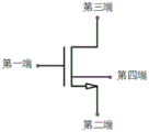
图1是本申请实施例提供的一种NMOS管的结构示意图;FIG. 1 is a schematic structural diagram of an NMOS transistor provided in an embodiment of the present application;
图2是本申请实施例提供的一种PMOS管的结构示意图;FIG. 2 is a schematic structural diagram of a PMOS transistor provided in an embodiment of the present application;
图3是本申请实施例提供的一种驱动电路的结构示意图;FIG. 3 is a schematic structural diagram of a driving circuit provided in an embodiment of the present application;
图4是本申请实施例提供的一种驱动电路的另一结构示意图;FIG. 4 is another structural schematic diagram of a driving circuit provided by an embodiment of the present application;
图5是本申请实施例提供的一种驱动电路的另一结构示意图;FIG. 5 is another structural schematic diagram of a driving circuit provided by an embodiment of the present application;
图6是本申请实施例提供的一种驱动控制电路的结构示意图;FIG. 6 is a schematic structural diagram of a drive control circuit provided by an embodiment of the present application;
图7是本申请实施例提供的另一种驱动控制电路的结构示意图;FIG. 7 is a schematic structural diagram of another driving control circuit provided by an embodiment of the present application;
图8是本申请实施例提供的基于图5的驱动电路的信号的波形示意图。FIG. 8 is a schematic waveform diagram of signals based on the driving circuit in FIG. 5 provided by the embodiment of the present application.
具体实施方式Detailed ways
为了本技术领域人员更好理解本申请的技术方案,下面结合本申请实施例中的附图,对本申请实施例中的技术方案进行清楚、完整地描述,显然,所描述的实施例仅是本申请的部分实施例,而并非全部的实施例。基于本申请实施例的描述,本领域技术人员在没有做出创造性劳动前提下所获得的所有其他实施例,都属于本申请所保护的范围。In order for those skilled in the art to better understand the technical solutions of the present application, the technical solutions in the embodiments of the present application are clearly and completely described below in conjunction with the drawings in the embodiments of the present application. Obviously, the described embodiments are only the present invention. Some, but not all, embodiments of the application. Based on the description of the embodiments of the present application, all other embodiments obtained by those skilled in the art without making creative efforts fall within the protection scope of the present application.
本申请的说明书和权利要求书及上述附图中的术语“第一”、“第二”等是用于区别不同对象,而不是用于描述特定顺序。此外,术语“包括”和“具有”以及它们任何变形,意图在于覆盖不排他的包含。例如,包含了一系列步骤或单元的过程、方法、软件、产品或设备没有限定于已列出的步骤或单元,而是还包括没有列出的步骤或单元,或还包括对于这些过程、方法、产品或设备固有的其他步骤或单元。The terms "first", "second" and the like in the specification and claims of the present application and the above drawings are used to distinguish different objects, rather than to describe a specific order. Furthermore, the terms "include" and "have", as well as any variations thereof, are intended to cover a non-exclusive inclusion. For example, a process, method, software, product, or device that includes a series of steps or units is not limited to the listed steps or units, but also includes steps or units that are not listed, or includes , other steps or units inherent in the product or equipment.
在本文中提及“实施例”意味着,结合实施例描述的特定特征、结构或特性可以包含在本申请的至少一个实施例中。在说明书中的各个位置出现该短语并不一定均是指相同的实施例,也不是与其它实施例互斥的独立的或备选的实施例。本领域技术人员显式地和隐式地理解的是,本文所描述的实施例可以与其它实施例相结合。Reference herein to an "embodiment" means that a particular feature, structure, or characteristic described in connection with the embodiment can be included in at least one embodiment of the present application. The occurrences of this phrase in various places in the specification are not necessarily all referring to the same embodiment, nor are separate or alternative embodiments mutually exclusive of other embodiments. It is understood explicitly and implicitly by those skilled in the art that the embodiments described herein can be combined with other embodiments.
下面结合附图对本申请实施例进行介绍,附图中相交导线的交叉处有圆点表示导线相接,交叉处无圆点表示导线不相接。The following describes the embodiments of the present application in conjunction with the accompanying drawings. In the drawings, dots at the intersections of intersecting conductors indicate that the conductors are connected, and no dots at the intersections indicate that the conductors are not connected.
为了更好地理解本申请实施例的方案,下面先对本申请实施例可能涉及的相关术语和概念进行介绍。In order to better understand the solutions of the embodiments of the present application, the following first introduces related terms and concepts that may be involved in the embodiments of the present application.
GaN器件:具有低导通电阻、高工作频率,能满足下一代电子装备对功率器件更大功率、更高频率、更小体积和更恶劣高温工作的要求。GaN功率元件整体性能更加优异,而且可以在硅基质上外延成长,在面积与整体成本考量上,也具有比碳化硅元件更划算的可能性,因此也被运用在高功率、高频率半导体元件中。GaN devices: With low on-resistance and high operating frequency, it can meet the requirements of next-generation electronic equipment for higher power, higher frequency, smaller volume and harsher high-temperature operation of power devices. The overall performance of GaN power components is better, and it can be epitaxially grown on a silicon substrate. In terms of area and overall cost, it is also more cost-effective than silicon carbide components, so it is also used in high-power, high-frequency semiconductor components. .
随着工艺的进步和缺陷率的不断降低,GaN在交直流电力转换、改变电压电平、并且以一定数量的函数确保可靠电力供应的电子电源中的优势越来越明显。电源设计人员正在重新思考电路的设计,试图寻找能充分发挥全新GaN晶体管潜能又能避免负面影响的方法来创造电源系统。思考这类问题时通常的思路是在现有组件中寻找解决方案—GaN开关,Si开关驱动器,高速开关控制器,以及功率电感器、变压器和电容器等总体设计中的部件。生产电源产品的集成电路(IC)制造商如果能用共同设计的器件提供系统级解决方案,甚至在模块封装中集成多个芯片,就能够大大提高电源设计可能性。With the advancement of technology and the continuous reduction of defect rate, the advantages of GaN in electronic power supplies for AC and DC power conversion, changing voltage levels, and ensuring reliable power supply with a certain number of functions are becoming more and more obvious. Power designers are rethinking circuit design, trying to find ways to create power systems that can take full advantage of the potential of the new GaN transistors without negative side effects. The usual way of thinking about these kinds of problems is to look for solutions in existing components—GaN switches, Si switch drivers, high-speed switch controllers, and parts in the overall design such as power inductors, transformers, and capacitors. Integrated circuit (IC) manufacturers producing power products can greatly expand power supply design possibilities if they can provide system-level solutions with co-designed devices, or even integrate multiple chips in a module package.
与硅Si基功率电子器件相比,GaN基功率电子器件具有如下3个优点:Compared with silicon Si-based power electronic devices, GaN-based power electronic devices have the following three advantages:
1、高效节能:由于GaN材料特有的极化特性,在AlGaN/GaN异质结间存在极强的极化效应,形成迁移率高达2000和面密度高达量级的高浓度二维电子气(2DEG)。GaN基功率开关器件HFET利用AlGaN/GaN异质结2DEG工作,器件具有导通电阻小、开关速度快的优点,使器件的通态损耗和开关大大降低。1. High efficiency and energy saving: Due to the unique polarization characteristics of GaN materials, there is a strong polarization effect between AlGaN/GaN heterojunctions, forming a high-concentration two-dimensional electron gas (2DEG) with a mobility as high as 2000 and an areal density as high as an order of magnitude. ). The GaN-based power switching device HFET uses AlGaN/GaN heterojunction 2DEG to work. The device has the advantages of small on-resistance and fast switching speed, which greatly reduces the on-state loss and switching of the device.
2、可以使电力电子装置小型化、轻量化,低成本化:GaN材料比Si具有更大的禁带宽度,使GaN器件可以工作在更高温度环境,因此,可简化甚至省去散热装置。此外,由于GaN器件具有高的开关频率,使得系统的无源器件电容电感的体积大大缩小。这些都使得GaN基电力电子装置能更小型化轻量化,大大降低系统制作成本。2. Miniaturization, light weight and low cost of power electronic devices: GaN material has a larger band gap than Si, so that GaN devices can work in a higher temperature environment, so the heat dissipation device can be simplified or even omitted. In addition, because the GaN device has a high switching frequency, the volume of the passive device capacitance and inductance of the system is greatly reduced. All of these make the GaN-based power electronic device more miniaturized and lightweight, greatly reducing the system manufacturing cost.
3、输出功率密度大,驱动力强劲:由于宽禁带等特性,GaN材料的临界击穿电场高达3.4MV/cm,是Si材料的10倍,因此,GaN器件具有更高耐压能力。同时,GaN基器件利用2DEG工作,获得低导通电阻,高电流密度,因此使GaN器件可以获得更大的功率密度。3. High output power density and strong driving force: Due to the characteristics of wide bandgap and other characteristics, the critical breakdown electric field of GaN material is as high as 3.4MV/cm, which is 10 times that of Si material. Therefore, GaN devices have higher withstand voltage capability. At the same time, GaN-based devices work with 2DEG to obtain low on-resistance and high current density, so that GaN devices can obtain greater power density.
与硅MOSFET,氮化镓基场效应晶体管(GaN)运行的速度快得多在较低的栅极阈值电压。此外,对于GaN FET的内部栅极电阻更低,体二极管的反向恢复特性远优于硅MOSFET。GaNFET有一些输出电容,但它明显低于硅。实际应用中,GaN晶体管具有较低的电阻(RDS(ON))和栅极电荷QG。更重要的是,GaN晶体管不受像MOSFET那样的强负温度系数的影响。因此,对于GaN FET的驱动要求,是否正常或关闭,将完全不同与硅MOSFET。Compared to silicon MOSFETs, Gallium Nitride-based Field Effect Transistors (GaN) operate much faster at lower gate threshold voltages. In addition, for the lower internal gate resistance of GaN FETs, the reverse recovery characteristics of the body diode are much better than those of silicon MOSFETs. GaNFETs have some output capacitance, but it's significantly lower than silicon. In practice, GaN transistors have lower resistance (RDS(ON)) and gate charge QG. What's more, GaN transistors are not subject to strong negative temperature coefficients like MOSFETs. Therefore, the driving requirements for a GaN FET, whether it is normal or off, will be completely different from that of a silicon MOSFET.
与传统Si驱动相比,GaN驱动电路驱动开关频率更高,要求的驱动电压更低,效率更高。对于电源设计人员来说,驱动GaN器件需要考虑的因素:Compared with the traditional Si driver, the GaN driver circuit drives the switching frequency higher, requires lower driving voltage, and has higher efficiency. For power supply designers, factors to consider when driving GaN devices:
(1)、低阈值电压(1), low threshold voltage
GaN FET的阈值电压一般低于1.5V,最小值低至0.7V,相比很多MOSFETs低,但它随温度几乎平缓变化。The threshold voltage of GaN FET is generally lower than 1.5V, the minimum value is as low as 0.7V, which is lower than that of many MOSFETs, but it changes almost smoothly with temperature.
(2)、栅源电压上限要求严格:VGS(MAX)=6V。一方面,VGS必须被设定在5.5V以下来预留0.5V的安全余量。另一方面,从Rds(ON)与VGS曲线看出,在VGS=4.5-5.5V时,RDS(ON)可以达到最小值,意味着降低传导损耗。综合考虑,将VGS设置在5V。栅源电压设计要求带来的问题:必须对栅源电压进行严格控制,避免损坏GaN FET功率管栅极,适用于MOSFETs驱动的普通偏置不能被直接使用。(2) The upper limit of the gate-source voltage is strictly required: VGS(MAX)=6V. On the one hand, VGS must be set below 5.5V to reserve a safety margin of 0.5V. On the other hand, it can be seen from the curve of Rds(ON) and VGS that when VGS=4.5-5.5V, RDS(ON) can reach the minimum value, which means that the conduction loss is reduced. All things considered, set VGS at 5V. Problems caused by the gate-source voltage design requirements: the gate-source voltage must be strictly controlled to avoid damage to the gate of the GaN FET power tube, and the common bias suitable for driving MOSFETs cannot be used directly.
(3)、EMI问题(3), EMI problem
由于GaN可以工作在较高的频率,所以,存在较大的dV/dt。这将会引起严重的EMI问题。Since GaN can work at a higher frequency, there is a larger dV/dt. This will cause serious EMI problems.
另外,本申请实施例中,如图1所示,针对NMOS管,NMOS管的第一端为栅极,第二端为源极,第三端为漏极,第四端为衬底,第四端接地;如图2所示,针对PMOS管,PMOS管的第一端为栅极,第二端为源极,第三端为漏极,第四端为衬底,第四端用于接入电源,如VDD;针对驱动控制模块,其第一端为DR,第二端为DU,第三端为DW。In addition, in the embodiment of the present application, as shown in FIG. 1 , for the NMOS transistor, the first end of the NMOS transistor is the gate, the second end is the source, the third end is the drain, the fourth end is the substrate, and the first end is the substrate. The four terminals are grounded; as shown in Figure 2, for the PMOS transistor, the first end of the PMOS transistor is the gate, the second end is the source, the third end is the drain, the fourth end is the substrate, and the fourth end is used for Connect to the power supply, such as VDD; for the drive control module, the first terminal is DR, the second terminal is DU, and the third terminal is DW.
相关技术中,如图3所示,图3为传统驱动的驱动控制电路,其驱动模块通过反向器链逐级驱动。输出电压驱动外部MOS功率管。外部MOS功率管在栅源之间有一个不可忽略的电容。为了快速的地导通或关断漏极电流,需要较大的电流来驱动栅极电压上升或者下降。驱动采用一段控制方式,Drive信号为0时,NMOS管N1栅极电压位置高。同时,N1打开输出大电流,瞬间GATE电压变高;同理,Drive信号为1时,NMOS管N2、N3被打开,瞬间拉低GATE电压。In the related art, as shown in FIG. 3 , FIG. 3 is a drive control circuit of a conventional drive, and its drive modules are driven step by step through an inverter chain. The output voltage drives an external MOS power transistor. The external MOS power transistor has a non-negligible capacitance between the gate and the source. In order to quickly turn on or turn off the drain current, a larger current is required to drive the gate voltage up or down. The drive adopts a one-stage control method. When the Drive signal is 0, the gate voltage of the NMOS transistor N1 is high. At the same time, N1 is turned on to output a large current, and the GATE voltage becomes higher instantly; similarly, when the Drive signal is 1, the NMOS transistors N2 and N3 are turned on, and the GATE voltage is pulled down instantly.
其中,基于图1所示的驱动电路的缺点是,驱动采用一段控制方式,开关过程中存在的di/dt变化大,导致EMI效果差。同时,输出电压受VCC电压的限制,最高为VCC-VGS,输出电压随着VCC的变化而变化,对于GaN驱动管是不利的。要想使用该驱动,就需要增加额外电路对VCC进行控制,从而增加成本。Among them, the disadvantage of the drive circuit shown in Figure 1 is that the drive adopts a one-stage control mode, and the di/dt changes during the switching process are large, resulting in poor EMI effects. At the same time, the output voltage is limited by the VCC voltage, the highest is VCC-VGS, and the output voltage changes with the change of VCC, which is unfavorable for the GaN drive tube. If you want to use this driver, you need to add an additional circuit to control VCC, which increases the cost.
进一步的,图4为谐振型驱动原理图的驱动电路,其核心思想是在驱动电路中加入LC谐振电路,利用开关管内部的寄生电容与外部电感谐振来实现开关管的驱动,并对储存在谐振电感中的能量进行有效回收,从而减小驱动损耗。但该控制电路复杂,需要增加额外电路对VCC进行控制,并且谐振型驱动只有在超高频场合才能发挥其优势。对于反激结构不适用。Further, Fig. 4 is the drive circuit of the resonant drive schematic diagram, the core idea is to add an LC resonant circuit to the drive circuit, and use the parasitic capacitance inside the switch tube to resonate with the external inductance to realize the drive of the switch tube, and store in The energy in the resonant inductor is effectively recovered, thereby reducing the driving loss. However, the control circuit is complicated, and an additional circuit needs to be added to control VCC, and the resonant drive can only exert its advantages in ultra-high frequency applications. Not applicable for flyback configurations.
进而,基于上述相关技术的缺陷,本申请实施例提供了一种驱动电路、芯片控制电路、电源适配器和电子设备,用于解决上述缺陷。Furthermore, based on the defects of the above-mentioned related technologies, the embodiments of the present application provide a driving circuit, a chip control circuit, a power adapter and an electronic device for solving the above-mentioned defects.
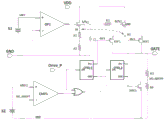
请参阅图5,图5是本申请实施例提供的一种驱动电路的结构示意图,所述驱动电路包括:运放电路OP1、比较器CMP1、第一NMOS管MN1、第二NMOS管MN2、第三NMOS管MN3、第一PMOS管MP1、第二PMOS管MP2、第一驱动控制模块CTRL1、第二驱动控制模块CTR2,其中,Please refer to FIG. 5. FIG. 5 is a schematic structural diagram of a driving circuit provided by an embodiment of the present application. The driving circuit includes: an operational amplifier circuit OP1, a comparator CMP1, a first NMOS transistor MN1, a second NMOS transistor MN2, a Three NMOS transistors MN3, the first PMOS transistor MP1, the second PMOS transistor MP2, the first drive control module CTRL1, and the second drive control module CTR2, wherein,
所述运放电路OP1的同相输入端(+)连接第一电源S1,所述运放电路OP1的输出端连接所述第一NMOS管MN1的第一端,所述第一NMOS管MN2的第三端连接第二电源VDD,所述第一MOS管MN1的第二端连接第一电阻R1的一端,所述第一电阻R1的另一端连接所述运放电路OP1的反相输入端(-)以及通过第二电阻R2进行接地;The non-inverting input terminal (+) of the operational amplifier circuit OP1 is connected to the first power supply S1, the output terminal of the operational amplifier circuit OP1 is connected to the first end of the first NMOS transistor MN1, and the first terminal of the first NMOS transistor MN2 The three terminals are connected to the second power supply VDD, the second terminal of the first MOS transistor MN1 is connected to one terminal of the first resistor R1, and the other terminal of the first resistor R1 is connected to the inverting input terminal of the operational amplifier circuit OP1 (- ) and grounding through the second resistor R2;
所述比较器CMP1的同相输入端(+)连接第三电源S2,所述比较器CMP1的输出端连接或门电路的第一输入端,所述或门电路的第二输入端用于接入驱动信号Drive_P,所述驱动信号Drive_P还被输入所述第一驱动控制模块CTRL1的第一端;The non-inverting input terminal (+) of the comparator CMP1 is connected to the third power supply S2, the output terminal of the comparator CMP1 is connected to the first input terminal of the OR gate circuit, and the second input terminal of the OR gate circuit is used to access a drive signal Drive_P, the drive signal Drive_P is also input to the first terminal of the first drive control module CTRL1;
所述或门电路的输出端连接所述第二驱动控制模块的第一端,所述第二驱动控制模块的第二端连接第二PMOS管MP2的第一端;所述第二PMOS管MP2的第二端连接所述第一PMOS管MP1的第二端以及所述第二NMOS端MN2的第二端,所述第二PMOS管MN2的第三端连接驱动端口GATE,所述驱动端口GATE用于驱动GaN功率管;所述第二NMOS管MN2的第三端还连接第三电阻R3的一端,第三电阻R3的另一端连接第四电阻R4的一端以及所述比较器CMP1的反相输入端(-);The output end of the OR gate circuit is connected to the first end of the second drive control module, and the second end of the second drive control module is connected to the first end of the second PMOS transistor MP2; the second PMOS transistor MP2 The second end of the first PMOS transistor MP1 is connected to the second end of the second NMOS end MN2, the third end of the second PMOS transistor MN2 is connected to the drive port GATE, and the drive port GATE Used to drive a GaN power transistor; the third end of the second NMOS transistor MN2 is also connected to one end of the third resistor R3, and the other end of the third resistor R3 is connected to one end of the fourth resistor R4 and the inverting phase of the comparator CMP1 input (-);
所述第二NMOS管MN2的第一端连接第五电阻R5的一端,所述第五电阻R5的另一端连接所述第一NMOS管NM1的第一端以及通过第一电容C1进行接地;所述第二NMOS管MN2的第三端连接所述第二电源VDD;The first end of the second NMOS transistor MN2 is connected to one end of the fifth resistor R5, and the other end of the fifth resistor R5 is connected to the first end of the first NMOS transistor NM1 and grounded through the first capacitor C1; The third end of the second NMOS transistor MN2 is connected to the second power supply VDD;
所述第一驱动控制模块CTRL1的第二端连接所述第一PMOS管MP1的第一端,所述第一驱动控制模块CTR1的第三端连接所述第三NMOS管MN3的第一端以及所述第二驱动控制模块CTR2的第三端,所述第三NMOS管MN3连接所述第二PMOS管MP2的第三端,所述第三NMOS管MN3的第二端接地。The second end of the first drive control module CTRL1 is connected to the first end of the first PMOS transistor MP1, the third end of the first drive control module CTR1 is connected to the first end of the third NMOS transistor MN3 and The third end of the second drive control module CTR2 and the third NMOS transistor MN3 are connected to the third end of the second PMOS transistor MP2, and the second end of the third NMOS transistor MN3 is grounded.
其中,R1、R2可以替换成一个可变电阻,通过该可变电阻调节R1与R2之间的比值。R3、R4也可以替换成一个可变电阻,通过该可变电阻调节R3与R4之间的比值。Wherein, R1 and R2 can be replaced with a variable resistor, and the ratio between R1 and R2 can be adjusted through the variable resistor. R3 and R4 can also be replaced with a variable resistor, through which the ratio between R3 and R4 can be adjusted.
可选的,所述运放电路OP1、所述第一电阻R1、所述第二电阻R2、所述第一NMOS管MN1用于形成LDO负反馈系统;Optionally, the operational amplifier circuit OP1, the first resistor R1, the second resistor R2, and the first NMOS transistor MN1 are used to form an LDO negative feedback system;
所述负反馈系统用于通过所述第一电阻R1、所述第二电阻R2之间的比值,以及所述运放电路OP1实现动态调节所述第一NMOS管MN1的电流,以得到所述第一NMOS管MN1的第二端的第一输出电压V1;The negative feedback system is used to dynamically adjust the current of the first NMOS transistor MN1 through the ratio between the first resistor R1 and the second resistor R2, and the operational amplifier circuit OP1, so as to obtain the the first output voltage V1 of the second terminal of the first NMOS transistor MN1;
当所述第一输出电压V1小于第一输出电压设计值时,所述运放电路OP1的输出变高,通过所述第一NMOS管NM1的电流增大,所述第一输出电压V1增加;When the first output voltage V1 is less than the first output voltage design value, the output of the operational amplifier circuit OP1 becomes high, the current passing through the first NMOS transistor NM1 increases, and the first output voltage V1 increases;
反之,当所述第一输出电压大于第一输出电压设计值时,所述运放电路的输出变低,通过所述第一NMOS管的电流减小,所述第一输出电压降低,从而实现动态调节所述第一NMOS管的第二端的第一输出电压。Conversely, when the first output voltage is greater than the first output voltage design value, the output of the operational amplifier circuit becomes low, the current passing through the first NMOS transistor decreases, and the first output voltage decreases, thereby realizing and dynamically adjusting the first output voltage of the second terminal of the first NMOS transistor.
其中,第一输出电压设计值可以预先设置或者系统默认,例如,第一输出电压设计值可以为设定值,即经验值。Wherein, the first design value of the output voltage may be preset or defaulted by the system, for example, the first design value of the output voltage may be a set value, that is, an empirical value.
可选的,所述第二NMOS管MN2的第二端的第二输出电压V2与所述第一输出电压V1之间的差值的绝对值小于预设阈值。Optionally, the absolute value of the difference between the second output voltage V2 of the second terminal of the second NMOS transistor MN2 and the first output voltage V1 is smaller than a preset threshold.
其中,预设阈值可以预先设置或者系统默认,预设阈值可以趋近于0,例如,预设阈值为0.01。Wherein, the preset threshold may be preset or defaulted by the system, and the preset threshold may be close to 0, for example, the preset threshold is 0.01.
可选的,所述第一输出电压V1由所述运放电路OP1的同相输入端(+)的输入电压VREF、所述第一电阻R1和所述第二电阻R2确定。具体计算公式如下:Optionally, the first output voltage V1 is determined by the input voltage VREF of the non-inverting input terminal (+) of the operational amplifier circuit OP1, the first resistor R1 and the second resistor R2. The specific calculation formula is as follows:
V1=VREF*(R1+R2)/R2V1=VREF*(R1+R2)/R2
可选的,所述第二输出电压V2由所述运放电路OP1的同相输入端(+)的输入电压VREF、所述第一电阻R1和所述第二电阻R2确定,具体计算公式如下:Optionally, the second output voltage V2 is determined by the input voltage VREF of the non-inverting input terminal (+) of the operational amplifier circuit OP1, the first resistor R1 and the second resistor R2, and the specific calculation formula is as follows:
V2=VREF*(R1+R2)/R2V2=VREF*(R1+R2)/R2
可选的,所述驱动信号Drive_P用于通过所述第一驱动控制模块CTRL1开启所述第一PMOS管MP1,且关闭所述第三NMOS管MN3,通过所述第三电阻R3和所述第四电阻R4分压,得到第三输出电压VO_ADOPT,将所述第三输出电压VO_ADOPT作为所述比较器CMP1的反相输入端(-)的第一输入信号,将所述比较器CMP1的同相输入端(+)的第二输入信号进行比较,得到驱动控制信号;将所述驱动控制信号与所述驱动信号Drive_P通过或门电路,得到输出信号,通过该输出信号开启所述第二PMOS管,由所述第一PMOS管MP1和所述第二PMOS管MP1同时充电。Optionally, the drive signal Drive_P is used to turn on the first PMOS transistor MP1 through the first drive control module CTRL1, and turn off the third NMOS transistor MN3, through the third resistor R3 and the first The four resistors R4 divide the voltage to obtain the third output voltage VO_ADOPT, and use the third output voltage VO_ADOPT as the first input signal of the inverting input terminal (-) of the comparator CMP1, and use the non-inverting input of the comparator CMP1 Compare the second input signal of terminal (+) to obtain a drive control signal; pass the drive control signal and the drive signal Drive_P through an OR gate circuit to obtain an output signal, and turn on the second PMOS transistor through the output signal, Charged simultaneously by the first PMOS transistor MP1 and the second PMOS transistor MP1.
可选的,所述第一驱动控制模块CTRL1包括M个反相器、第四NMOS管MN4、第五NMOS管MN5、第三PMOS管MP3和第四PMOS管MP4,所述M为偶数;Optionally, the first drive control module CTRL1 includes M inverters, a fourth NMOS transistor MN4, a fifth NMOS transistor MN5, a third PMOS transistor MP3, and a fourth PMOS transistor MP4, where M is an even number;
所述第一驱动控制模块CTRL1的第一端通过所述M个反相器连接所述第一驱动控制模块CTRL1的第二端以及所述第五NMOS管MN5的第一端;所述第五NMOS管MN5的第二端接地;The first end of the first drive control module CTRL1 is connected to the second end of the first drive control module CTRL1 and the first end of the fifth NMOS transistor MN5 through the M inverters; The second end of the NMOS transistor MN5 is grounded;
所述第一驱动控制模块CTRL1的第一端连接所述第四NMOS管MN4的第一端,所述第四NMOS管MN4的第二端接地,所述第四NMOS管MN4的第三端连接第六电阻R6的一端,所述第六电阻R6的另一端连接所述第三PMOS管MP3的第三端和第一端,所述第三PMOS管MP3的第一端连接所述第四PMOS管MP4的第一端;所述第四PMOS管MP4的第三端连接第七电阻R7的一端,所述第七电阻R7的另一端连接所述第一驱动控制模块CTRL1的第三端以及所述第五NMOS管MN5的第三端;所述第三PMOS管MP3的第二端和所述第四PMOS管MP4的第二端均连接所述第二电源VDD。The first end of the first drive control module CTRL1 is connected to the first end of the fourth NMOS transistor MN4, the second end of the fourth NMOS transistor MN4 is grounded, and the third end of the fourth NMOS transistor MN4 is connected to One end of the sixth resistor R6, the other end of the sixth resistor R6 is connected to the third end and the first end of the third PMOS transistor MP3, and the first end of the third PMOS transistor MP3 is connected to the fourth PMOS transistor MP3 The first end of the tube MP4; the third end of the fourth PMOS transistor MP4 is connected to one end of the seventh resistor R7, and the other end of the seventh resistor R7 is connected to the third end of the first drive control module CTRL1 and the The third end of the fifth NMOS transistor MN5; the second end of the third PMOS transistor MP3 and the second end of the fourth PMOS transistor MP4 are both connected to the second power supply VDD.
具体的,如图6所示,图6中,M=4,即以4个反相器为例进行说明,图中以三角形代表反相器。反相器一方面能够提升驱动能力,另一方面,能够实现延时效果。Specifically, as shown in FIG. 6 , in FIG. 6 , M=4, that is, four inverters are taken as an example for illustration, and the inverters are represented by triangles in the figure. On the one hand, the inverter can improve the driving ability, on the other hand, it can realize the delay effect.
可选的,所述第二驱动控制模块CTRL2包括N个反相器、第六NMOS管MN6、第七NMOS管MN7、第五PMOS管MP5和第六PMOS管MP6,所述N为偶数;Optionally, the second drive control module CTRL2 includes N inverters, a sixth NMOS transistor MN6, a seventh NMOS transistor MN7, a fifth PMOS transistor MP5, and a sixth PMOS transistor MP6, where N is an even number;
所述第二驱动控制模块CTRL2的第一端通过所述N个反相器连接所述第二驱动控制模块CTRL2的第二端以及所述第七NMOS管MN7的第一端;所述第七NMOS管MN7的第二端接地;The first end of the second drive control module CTRL2 is connected to the second end of the second drive control module CTRL2 and the first end of the seventh NMOS transistor MN7 through the N inverters; the seventh The second end of the NMOS transistor MN7 is grounded;
所述第二驱动控制模块CTRL的第一端连接所述第六NMOS管MN6的第一端,所述第六NMOS管MN6的第二端接地,所述第六NMOS管MN6的第三端连接第八电阻R8的一端,所述第八电阻R8的另一端连接所述第五PMOS管MP5的第三端和第一端,所述第五PMOS管MP5的第一端连接所述第六PMOS管MP6的第一端;所述第六PMOS管MP6的第三端连接第九电阻R9的一端,所述第九电阻R9的另一端连接所述第二驱动控制模块CTRL2的第三端以及所述第七NMOS管MN7的第三端;所述第五PMOS管MP5的第二端和所述第六PMOS管MP6的第二端均连接所述第二电源VDD。The first end of the second drive control module CTRL is connected to the first end of the sixth NMOS transistor MN6, the second end of the sixth NMOS transistor MN6 is grounded, and the third end of the sixth NMOS transistor MN6 is connected to One end of the eighth resistor R8, the other end of the eighth resistor R8 is connected to the third end and the first end of the fifth PMOS transistor MP5, and the first end of the fifth PMOS transistor MP5 is connected to the sixth PMOS transistor MP5 The first end of the transistor MP6; the third end of the sixth PMOS transistor MP6 is connected to one end of the ninth resistor R9, and the other end of the ninth resistor R9 is connected to the third end of the second drive control module CTRL2 and the The third end of the seventh NMOS transistor MN7; the second end of the fifth PMOS transistor MP5 and the second end of the sixth PMOS transistor MP6 are both connected to the second power supply VDD.
具体的,如图7所示,图7中,N=4,即以4个反相器为例进行说明,图中以三角形代表反相器。反相器一方面能够提升驱动能力,另一方面,能够实现延时效果。Specifically, as shown in FIG. 7 , in FIG. 7 , N=4, that is, four inverters are taken as an example for illustration, and the inverters are represented by triangles in the figure. On the one hand, the inverter can improve the driving ability, on the other hand, it can realize the delay effect.
本申请实施例,由于或门电路的控制,实现不同时段分别控制第一驱动控制电路和第二驱动控制电路进行工作,进而,形成两段驱动控制,采用两段驱动控制和LDO运放钳位输出驱动电压上限技术,既改善了EMI,又提高了芯片驱动电压的精确值,避免了因为输出电压值的波动而损坏GaN器件。进而,能够在满足GaN驱动要求的基础上,又改善芯片EMI的效果。In the embodiment of the present application, due to the control of the OR gate circuit, the first drive control circuit and the second drive control circuit are respectively controlled to work in different periods, and then two-stage drive control is formed, and the two-stage drive control and LDO operational amplifier are used to clamp The upper limit technology of the output driving voltage not only improves the EMI, but also improves the precise value of the chip driving voltage, avoiding damage to the GaN device due to the fluctuation of the output voltage value. Furthermore, the effect of chip EMI can be improved on the basis of satisfying GaN driving requirements.
具体实现中,运放OP1、电阻R1和R2,NMOS管MN1构成了LDO电路。In specific implementation, the operational amplifier OP1, the resistors R1 and R2, and the NMOS tube MN1 form an LDO circuit.
针对上述驱动电路,其具体工作原理:LDO是一个负反馈的系统,利用R1和R2的比值,以及运放动态调节通过MN1的电流,可以实现输出电压(V1)精确值。当输出电压V1小于设计值时,OP1输出变高,通过MN1的电流增大,输出电压V1增加,当输出电压V1大于设计值时,OP1输出变低,通过MN1的电流减小,输出电压V1减小。从而实现V1电压输出维持在设计值。同样的,将MN2和MN1的第一端口接在一起,两者尽量匹配,可以实现输出电压V2维持在设计值,即V1与V2两者相等或者几乎相等。电容C1的作用是稳定MOS管栅级的电压,降低LDO的带宽,增加LDO系统的稳定性。同时,C1和R5组成了一个低通滤波器,可以减少MN2栅极电压对MN1栅极电压的影响。For the above drive circuit, its specific working principle: LDO is a negative feedback system, using the ratio of R1 and R2, and the op amp to dynamically adjust the current through MN1, the precise value of the output voltage (V1) can be achieved. When the output voltage V1 is lower than the design value, the output of OP1 becomes high, the current through MN1 increases, and the output voltage V1 increases. When the output voltage V1 is greater than the design value, the output of OP1 becomes low, the current through MN1 decreases, and the output voltage V1 decrease. In this way, the voltage output of V1 is maintained at the design value. Similarly, the first ports of MN2 and MN1 are connected together, and the two are matched as much as possible, so that the output voltage V2 can be maintained at the design value, that is, V1 and V2 are equal or almost equal. The function of the capacitor C1 is to stabilize the voltage of the gate of the MOS transistor, reduce the bandwidth of the LDO, and increase the stability of the LDO system. At the same time, C1 and R5 form a low-pass filter, which can reduce the influence of the gate voltage of MN2 on the gate voltage of MN1.
其中,上述设定值可以根据需要驱动的设备的GAN功放的驱动电压确定。Wherein, the above set value may be determined according to the driving voltage of the GAN power amplifier of the device to be driven.
具体实现中,两段驱动工作原理:首先,驱动信号Drive_P通过驱动控制模块CTRL1(电路如图6所示),开启MP1,关闭MN3,使输出电压上升。然后,通过电阻R3和R4分压,采样输出电压。采样后的输出电压通过比较器CMP1与基准电压VREF1比较输出2段驱动控制信号。再和信号Drive_P相或,通过控制模块CTRL2开启PM2,最后由MP1和MP2同时给出充电。这样使驱动电流由小到大变化,驱动电压从低到高有一个缓慢渐变的过程。降低了di/dt尖冲,改善了EMI效果。In the specific implementation, the working principle of the two-stage drive is: first, the drive signal Drive_P passes through the drive control module CTRL1 (the circuit is shown in Figure 6), turns on MP1, turns off MN3, and increases the output voltage. Then, divide the voltage through resistors R3 and R4 to sample the output voltage. The sampled output voltage is compared with the reference voltage VREF1 by the comparator CMP1 to output 2-stage drive control signals. Then it is ORed with the signal Drive_P, PM2 is turned on through the control module CTRL2, and finally MP1 and MP2 give charging at the same time. In this way, the driving current changes from small to large, and the driving voltage has a slow and gradual process from low to high. Reduced di/dt spike and improved EMI effect.
本申请实施例中,针对GaN器件的驱动要求,采用LDO运放钳位输出驱动电压上限的控制方法,确保输出驱动电压上线严格的钳位在6V左右。同时,采用检测输出驱动电压的大小2段驱动的方法,改善EMI效果。即能够满足GaN驱动要求,使输出驱动电压很好的维持在6V,避免输出电压波动对GaN造成损坏,又改善芯片EMI的效果。图5所示的驱动电路与图3所示的驱动电路相比较,本申请实施例具备EMI更小,且成本更低;图5所示的驱动电路与图4所示的驱动电路相比较,本申请实施例具备EMI更小,而且能够适用于反激结构。In the embodiment of this application, according to the driving requirements of the GaN device, the control method of clamping the upper limit of the output driving voltage of the LDO operational amplifier is adopted to ensure that the upper line of the output driving voltage is strictly clamped at about 6V. At the same time, the EMI effect is improved by using the method of detecting the magnitude of the output driving voltage and driving in two stages. That is, it can meet the driving requirements of GaN, so that the output driving voltage can be well maintained at 6V, avoiding damage to GaN caused by output voltage fluctuations, and improving the effect of chip EMI. Compared with the driving circuit shown in Figure 5, the driving circuit shown in Figure 5 has a smaller EMI and lower cost in the embodiment of the present application; the driving circuit shown in Figure 5 is compared with the driving circuit shown in Figure 4, The embodiment of the present application has lower EMI and is applicable to a flyback structure.
其中,第一电源、第三电源均可以是AC/DC电源、DC/DC电源、稳压电源、通信电源、模块电源、变频电源、逆变电源、交流稳压电源、直流稳压电源等,本申请实施例对此不做限定。第一电源、第二电源可以为相同的电源或者不同的电源。Wherein, both the first power supply and the third power supply can be AC/DC power supply, DC/DC power supply, regulated power supply, communication power supply, module power supply, variable frequency power supply, inverter power supply, AC regulated power supply, DC regulated power supply, etc. This embodiment of the present application does not limit it. The first power supply and the second power supply may be the same power supply or different power supplies.
进一步地,通过GaN功率管输出给用电设备,用于实现对用电设备进行充电,用电设备可以理解为需要用户进行充电的设备,用户设备可以包括但不仅限于:智能手机、平板电脑、智能机器人、智能电梯、车载设备、可穿戴设备、智能家居设备、计算设备或连接到无线调制解调器的其他处理设备,以及各种形式的用户设备(user equipment,UE),移动台(mobile station,MS),终端设备(terminaldevice)等等。Further, the GaN power tube is used to output to the electric device to charge the electric device. The electric device can be understood as a device that needs to be charged by the user. The user device can include but not limited to: smart phones, tablet computers, Smart robots, smart elevators, in-vehicle devices, wearable devices, smart home devices, computing devices or other processing devices connected to wireless modems, and various forms of user equipment (user equipment, UE), mobile station (mobile station, MS ), terminal device (terminaldevice) and so on.
具体实现中,如图8所示,其中,示出了Drive_P、DU1、DU2以及GATE信号的波形图,可以看到能够使驱动电流由小到大变化,驱动电压从低到高有一个缓慢渐变的过程。降低了di/dt尖冲,改善了EMI效果。In the specific implementation, as shown in Figure 8, which shows the waveform diagram of Drive_P, DU1, DU2 and GATE signals, it can be seen that the driving current can be changed from small to large, and the driving voltage has a slow gradient from low to high the process of. Reduced di/dt spike and improved EMI effect.
进一步的,上述驱动电路可以应用于控制芯片电路,该控制芯片电路可以包括以下至少一种:AC-DC芯片控制电路、DC-DC芯片控制电路,在此不做限定,AC-DC芯片控制电路可以为反激AC-DC芯片控制电路或者非反激AC-DC芯片控制电路。Further, the above driving circuit can be applied to a control chip circuit, and the control chip circuit can include at least one of the following: AC-DC chip control circuit, DC-DC chip control circuit, which is not limited here, AC-DC chip control circuit It can be a flyback AC-DC chip control circuit or a non-flyback AC-DC chip control circuit.
如此,具体实现中,采用两段驱动控制和LDO运放钳位输出驱动电压上限技术,既改善了EMI,又提高了芯片驱动电压的精确值,避免了因为输出电压值的波动而损坏GaN器件。例如,将该驱动用在反激ACDC控制芯片电路中,实现对GaN功率管的驱动。In this way, in the specific implementation, the two-stage drive control and LDO operational amplifier clamp output drive voltage upper limit technology are used, which not only improves EMI, but also improves the precise value of the chip drive voltage, avoiding damage to GaN devices due to fluctuations in output voltage values . For example, the driver is used in the flyback ACDC control chip circuit to realize the driving of the GaN power tube.
再进一步的,上述驱动电路以及上述控制芯片电路均可以应用于电源适配器。Still further, both the above-mentioned drive circuit and the above-mentioned control chip circuit can be applied to a power adapter.
当然,本申请实施例还提供一种电子设备,该电子设备可以包括如图5所描述的驱动电路或者芯片控制电路或者电源适配器,例如,电子设备可以为充电宝或者充电器。Certainly, the embodiment of the present application also provides an electronic device, which may include a drive circuit or a chip control circuit or a power adapter as described in FIG. 5 , for example, the electronic device may be a power bank or a charger.
以上是本申请实施例的实施方式,应当指出,对于本技术领域的普通技术人员来说,在不脱离本申请实施例原理的前提下,还可以做出若干改进和润饰,这些改进和润饰也视为本申请的保护范围。The above is the implementation of the embodiment of the present application. It should be pointed out that for those of ordinary skill in the art, without departing from the principle of the embodiment of the present application, some improvements and modifications can also be made. These improvements and modifications are also It is regarded as the scope of protection of this application.
Claims (10)
Priority Applications (1)
| Application Number | Priority Date | Filing Date | Title |
|---|---|---|---|
| CN202210109729.7A CN116015022B (en) | 2021-10-22 | 2021-10-22 | Drive circuits and related control chip circuits, power adapters and electronic devices |
Applications Claiming Priority (2)
| Application Number | Priority Date | Filing Date | Title |
|---|---|---|---|
| CN202210109729.7A CN116015022B (en) | 2021-10-22 | 2021-10-22 | Drive circuits and related control chip circuits, power adapters and electronic devices |
| CN202111230436.6A CN113676025B (en) | 2021-10-22 | 2021-10-22 | Drive circuit, control chip circuit, power adapter and electronic equipment |
Related Parent Applications (1)
| Application Number | Title | Priority Date | Filing Date |
|---|---|---|---|
| CN202111230436.6A Division CN113676025B (en) | 2021-10-22 | 2021-10-22 | Drive circuit, control chip circuit, power adapter and electronic equipment |
Publications (2)
| Publication Number | Publication Date |
|---|---|
| CN116015022A true CN116015022A (en) | 2023-04-25 |
| CN116015022B CN116015022B (en) | 2026-04-21 |
Family
ID=78550852
Family Applications (2)
| Application Number | Title | Priority Date | Filing Date |
|---|---|---|---|
| CN202111230436.6A Active CN113676025B (en) | 2021-10-22 | 2021-10-22 | Drive circuit, control chip circuit, power adapter and electronic equipment |
| CN202210109729.7A Active CN116015022B (en) | 2021-10-22 | 2021-10-22 | Drive circuits and related control chip circuits, power adapters and electronic devices |
Family Applications Before (1)
| Application Number | Title | Priority Date | Filing Date |
|---|---|---|---|
| CN202111230436.6A Active CN113676025B (en) | 2021-10-22 | 2021-10-22 | Drive circuit, control chip circuit, power adapter and electronic equipment |
Country Status (2)
| Country | Link |
|---|---|
| CN (2) | CN113676025B (en) |
| WO (1) | WO2023065829A1 (en) |
Families Citing this family (1)
| Publication number | Priority date | Publication date | Assignee | Title |
|---|---|---|---|---|
| CN113676025B (en) * | 2021-10-22 | 2022-02-08 | 深圳英集芯科技股份有限公司 | Drive circuit, control chip circuit, power adapter and electronic equipment |
Citations (5)
| Publication number | Priority date | Publication date | Assignee | Title |
|---|---|---|---|---|
| CN106788357A (en) * | 2017-01-23 | 2017-05-31 | 上海贝岭股份有限公司 | Drive circuit |
| CN110417393A (en) * | 2019-07-11 | 2019-11-05 | 杭州宽福科技有限公司 | Power tube drive circuit |
| CN111614245A (en) * | 2019-02-22 | 2020-09-01 | 德克萨斯仪器股份有限公司 | Enhanced Startup Circuit with JFET Emulation |
| US10911045B1 (en) * | 2020-04-03 | 2021-02-02 | University Of Electronic Science And Technology Of China | Segmented direct gate drive circuit of a depletion mode GaN power device |
| CN113676025B (en) * | 2021-10-22 | 2022-02-08 | 深圳英集芯科技股份有限公司 | Drive circuit, control chip circuit, power adapter and electronic equipment |
Family Cites Families (8)
| Publication number | Priority date | Publication date | Assignee | Title |
|---|---|---|---|---|
| JP5777537B2 (en) * | 2012-02-17 | 2015-09-09 | 三菱電機株式会社 | Power device control circuit and power device circuit |
| CN202856608U (en) * | 2012-05-24 | 2013-04-03 | 意法半导体研发(深圳)有限公司 | Power drive circuit |
| US20160079904A1 (en) * | 2013-04-17 | 2016-03-17 | Otis Elevator Company | Drive unit employing gallium nitride switches |
| US9571093B2 (en) * | 2014-09-16 | 2017-02-14 | Navitas Semiconductor, Inc. | Half bridge driver circuits |
| CN105871180B (en) * | 2016-04-08 | 2018-07-17 | 厦门大学 | A kind of high current CMOS push-pull driver circuits and its control method |
| CN110417243B (en) * | 2019-08-05 | 2021-06-22 | 上海航天电子通讯设备研究所 | High-voltage MOSFET (metal-oxide-semiconductor field effect transistor) driving circuit |
| CN111224647B (en) * | 2020-03-13 | 2024-11-29 | 无锡硅动力微电子股份有限公司 | High-reliability GaN power tube fast gate electrode driving circuit |
| CN111478562A (en) * | 2020-05-09 | 2020-07-31 | 上海坤振集成电路有限公司 | Power switching tube sectional driving circuit and method |
-
2021
- 2021-10-22 CN CN202111230436.6A patent/CN113676025B/en active Active
- 2021-10-22 CN CN202210109729.7A patent/CN116015022B/en active Active
-
2022
- 2022-08-30 WO PCT/CN2022/115740 patent/WO2023065829A1/en not_active Ceased
Patent Citations (5)
| Publication number | Priority date | Publication date | Assignee | Title |
|---|---|---|---|---|
| CN106788357A (en) * | 2017-01-23 | 2017-05-31 | 上海贝岭股份有限公司 | Drive circuit |
| CN111614245A (en) * | 2019-02-22 | 2020-09-01 | 德克萨斯仪器股份有限公司 | Enhanced Startup Circuit with JFET Emulation |
| CN110417393A (en) * | 2019-07-11 | 2019-11-05 | 杭州宽福科技有限公司 | Power tube drive circuit |
| US10911045B1 (en) * | 2020-04-03 | 2021-02-02 | University Of Electronic Science And Technology Of China | Segmented direct gate drive circuit of a depletion mode GaN power device |
| CN113676025B (en) * | 2021-10-22 | 2022-02-08 | 深圳英集芯科技股份有限公司 | Drive circuit, control chip circuit, power adapter and electronic equipment |
Also Published As
| Publication number | Publication date |
|---|---|
| CN113676025B (en) | 2022-02-08 |
| CN113676025A (en) | 2021-11-19 |
| WO2023065829A1 (en) | 2023-04-27 |
| CN116015022B (en) | 2026-04-21 |
Similar Documents
| Publication | Publication Date | Title |
|---|---|---|
| US9379620B2 (en) | Zero voltage soft switching scheme for power converters | |
| US8054110B2 (en) | Driver circuit for gallium nitride (GaN) heterojunction field effect transistors (HFETs) | |
| Umegami et al. | A novel high-efficiency gate drive circuit for normally off-type GaN FET | |
| US8237422B2 (en) | Efficient switch cascode architecture for switching devices | |
| US6212084B1 (en) | Active rectifier | |
| WO2014012518A1 (en) | Switching power supply and chip for controlling the same | |
| Kinzer et al. | Monolithic HV GaN power ICs: performance and application | |
| JP2024542014A (en) | Multilevel Power Converter Protection | |
| WO2023229900A1 (en) | Charging circuit for bootstrap capacitors | |
| CN114629358A (en) | Synchronous Rectification Gate Driver with Active Clamp | |
| TWI425730B (en) | Power switching device with complete drain-source voltage clamp and device and method for limiting maximum drain-source voltage of main switch field effect transistor of coupling-pull push-pull rectifier | |
| WO2023065789A1 (en) | Drive circuit and related product | |
| CN114337304A (en) | Control chip and built-in MOS tube driving speed control method thereof | |
| CN105575941B (en) | The high power resonant vibration power supply control chip that a kind of dual chip encapsulation is realized | |
| WO2023065829A1 (en) | Driving circuit, control chip circuit, power adapter, and electronic device | |
| Ming et al. | A GaN HEMT gate driver IC with programmable turn-on dV/dt control | |
| US20190348408A1 (en) | Multiphase Parallel DCDC Circuit and Chip Structure Thereof | |
| CN221575141U (en) | Driving circuit of switching device and switching power supply | |
| CN204465496U (en) | An isolated high-side driver | |
| CN113206542A (en) | Electrical converter system and method of manufacturing the same | |
| CN218867915U (en) | Protection circuit for SiC MOSFET | |
| US10651763B2 (en) | Radio-frequency/direct-current converter | |
| CN107437894B (en) | Overvoltage protection device | |
| Nagai et al. | A compact drive-by-microwave gate driver with coupler integrated in a package | |
| CN119030294B (en) | Medium-voltage silicon carbide module active gate driver with status feedback |
Legal Events
| Date | Code | Title | Description |
|---|---|---|---|
| PB01 | Publication | ||
| PB01 | Publication | ||
| SE01 | Entry into force of request for substantive examination | ||
| SE01 | Entry into force of request for substantive examination | ||
| GR01 | Patent grant |