CN115516628A - AI chip - Google Patents
AI chip Download PDFInfo
- Publication number
- CN115516628A CN115516628A CN202180029687.XA CN202180029687A CN115516628A CN 115516628 A CN115516628 A CN 115516628A CN 202180029687 A CN202180029687 A CN 202180029687A CN 115516628 A CN115516628 A CN 115516628A
- Authority
- CN
- China
- Prior art keywords
- die
- memory
- dies
- chip
- arithmetic
- Prior art date
- Legal status (The legal status is an assumption and is not a legal conclusion. Google has not performed a legal analysis and makes no representation as to the accuracy of the status listed.)
- Pending
Links
Images


Classifications
-
- H—ELECTRICITY
- H10—SEMICONDUCTOR DEVICES; ELECTRIC SOLID-STATE DEVICES NOT OTHERWISE PROVIDED FOR
- H10D—INORGANIC ELECTRIC SEMICONDUCTOR DEVICES
- H10D88/00—Three-dimensional [3D] integrated devices
-
- G—PHYSICS
- G06—COMPUTING OR CALCULATING; COUNTING
- G06F—ELECTRIC DIGITAL DATA PROCESSING
- G06F15/00—Digital computers in general; Data processing equipment in general
- G06F15/76—Architectures of general purpose stored program computers
- G06F15/78—Architectures of general purpose stored program computers comprising a single central processing unit
- G06F15/7839—Architectures of general purpose stored program computers comprising a single central processing unit with memory
- G06F15/7864—Architectures of general purpose stored program computers comprising a single central processing unit with memory on more than one IC chip
-
- G—PHYSICS
- G11—INFORMATION STORAGE
- G11C—STATIC STORES
- G11C5/00—Details of stores covered by group G11C11/00
- G11C5/02—Disposition of storage elements, e.g. in the form of a matrix array
-
- H—ELECTRICITY
- H10—SEMICONDUCTOR DEVICES; ELECTRIC SOLID-STATE DEVICES NOT OTHERWISE PROVIDED FOR
- H10B—ELECTRONIC MEMORY DEVICES
- H10B80/00—Assemblies of multiple devices comprising at least one memory device covered by this subclass
-
- H—ELECTRICITY
- H10—SEMICONDUCTOR DEVICES; ELECTRIC SOLID-STATE DEVICES NOT OTHERWISE PROVIDED FOR
- H10D—INORGANIC ELECTRIC SEMICONDUCTOR DEVICES
- H10D89/00—Aspects of integrated devices not covered by groups H10D84/00 - H10D88/00
- H10D89/10—Integrated device layouts
-
- H—ELECTRICITY
- H10—SEMICONDUCTOR DEVICES; ELECTRIC SOLID-STATE DEVICES NOT OTHERWISE PROVIDED FOR
- H10W—GENERIC PACKAGES, INTERCONNECTIONS, CONNECTORS OR OTHER CONSTRUCTIONAL DETAILS OF DEVICES COVERED BY CLASS H10
- H10W70/00—Package substrates; Interposers; Redistribution layers [RDL]
- H10W70/60—Insulating or insulated package substrates; Interposers; Redistribution layers
- H10W70/611—Insulating or insulated package substrates; Interposers; Redistribution layers for connecting multiple chips together
-
- H—ELECTRICITY
- H10—SEMICONDUCTOR DEVICES; ELECTRIC SOLID-STATE DEVICES NOT OTHERWISE PROVIDED FOR
- H10W—GENERIC PACKAGES, INTERCONNECTIONS, CONNECTORS OR OTHER CONSTRUCTIONAL DETAILS OF DEVICES COVERED BY CLASS H10
- H10W90/00—Package configurations
-
- H—ELECTRICITY
- H10—SEMICONDUCTOR DEVICES; ELECTRIC SOLID-STATE DEVICES NOT OTHERWISE PROVIDED FOR
- H10W—GENERIC PACKAGES, INTERCONNECTIONS, CONNECTORS OR OTHER CONSTRUCTIONAL DETAILS OF DEVICES COVERED BY CLASS H10
- H10W90/00—Package configurations
- H10W90/20—Configurations of stacked chips
- H10W90/293—Configurations of stacked chips characterised by non-galvanic coupling between the chips, e.g. capacitive coupling
-
- H—ELECTRICITY
- H10—SEMICONDUCTOR DEVICES; ELECTRIC SOLID-STATE DEVICES NOT OTHERWISE PROVIDED FOR
- H10W—GENERIC PACKAGES, INTERCONNECTIONS, CONNECTORS OR OTHER CONSTRUCTIONAL DETAILS OF DEVICES COVERED BY CLASS H10
- H10W90/00—Package configurations
- H10W90/20—Configurations of stacked chips
- H10W90/297—Configurations of stacked chips characterised by the through-semiconductor vias [TSVs] in the stacked chips
-
- H—ELECTRICITY
- H10—SEMICONDUCTOR DEVICES; ELECTRIC SOLID-STATE DEVICES NOT OTHERWISE PROVIDED FOR
- H10W—GENERIC PACKAGES, INTERCONNECTIONS, CONNECTORS OR OTHER CONSTRUCTIONAL DETAILS OF DEVICES COVERED BY CLASS H10
- H10W90/00—Package configurations
- H10W90/701—Package configurations characterised by the relative positions of pads or connectors relative to package parts
- H10W90/721—Package configurations characterised by the relative positions of pads or connectors relative to package parts of bump connectors
- H10W90/722—Package configurations characterised by the relative positions of pads or connectors relative to package parts of bump connectors between stacked chips
-
- H—ELECTRICITY
- H10—SEMICONDUCTOR DEVICES; ELECTRIC SOLID-STATE DEVICES NOT OTHERWISE PROVIDED FOR
- H10W—GENERIC PACKAGES, INTERCONNECTIONS, CONNECTORS OR OTHER CONSTRUCTIONAL DETAILS OF DEVICES COVERED BY CLASS H10
- H10W90/00—Package configurations
- H10W90/701—Package configurations characterised by the relative positions of pads or connectors relative to package parts
- H10W90/721—Package configurations characterised by the relative positions of pads or connectors relative to package parts of bump connectors
- H10W90/724—Package configurations characterised by the relative positions of pads or connectors relative to package parts of bump connectors between a chip and a stacked insulating package substrate, interposer or RDL
Landscapes
- Engineering & Computer Science (AREA)
- Theoretical Computer Science (AREA)
- Computer Hardware Design (AREA)
- Physics & Mathematics (AREA)
- General Engineering & Computer Science (AREA)
- General Physics & Mathematics (AREA)
- Design And Manufacture Of Integrated Circuits (AREA)
- Biophysics (AREA)
- Biomedical Technology (AREA)
- Health & Medical Sciences (AREA)
- Life Sciences & Earth Sciences (AREA)
- Artificial Intelligence (AREA)
- Molecular Biology (AREA)
- Computing Systems (AREA)
- Computational Linguistics (AREA)
- Neurology (AREA)
- Mathematical Physics (AREA)
- Software Systems (AREA)
- General Health & Medical Sciences (AREA)
- Evolutionary Computation (AREA)
- Data Mining & Analysis (AREA)
- Semiconductor Memories (AREA)
- Semiconductor Integrated Circuits (AREA)
Abstract
AI芯片(1)具备:存储数据的多个存储器裸片(200,201);进行AI处理中包括的运算的多个运算裸片(300,301);以及系统芯片(100),对多个存储器裸片(200,201)以及多个运算裸片(300,301)进行控制。多个存储器裸片(200,201)分别具有第1布局图案。多个运算裸片(300,301)分别具有第2布局图案。存储器裸片(201)被层叠在存储器裸片(200)的第1布局图案的上方。运算裸片(301)被层叠在运算裸片(300)的第2布局图案的上方。

The AI chip (1) has: a plurality of memory dies (200, 201) for storing data; a plurality of computing dies (300, 301) for performing calculations included in AI processing; and a system chip (100) for a plurality of A memory die (200, 201) and a plurality of computing dies (300, 301) are controlled. A plurality of memory dies (200, 201) each have a first layout pattern. Each of the plurality of computing dies (300, 301) has a second layout pattern. A memory die (201) is stacked over the first layout pattern of the memory die (200). The arithmetic die (301) is stacked on the second layout pattern of the arithmetic die (300).
Description
技术领域technical field
本公开涉及AI芯片。This disclosure relates to AI chips.
背景技术Background technique
专利文献1公开了一种层叠有具备多个逻辑宏单元电路的系统级芯片、以及具有由各逻辑宏单元电路访问的存储区的存储芯片的半导体集成电路装置。该半导体集成电路装置能够层叠多个存储芯片,并且能够增加存储容量。Patent Document 1 discloses a semiconductor integrated circuit device in which a system-on-chip including a plurality of logic macrocell circuits and a memory chip having a storage area accessed by each logic macrocell circuit are stacked. In this semiconductor integrated circuit device, a plurality of memory chips can be stacked, and the storage capacity can be increased.
(现有技术文献)(Prior art literature)
(专利文献)(patent documents)
专利文献1:国际公开第2010/021410号Patent Document 1: International Publication No. 2010/021410
近年来,期待高速进行利用了人工智能(AI:Artificial Intelligence)的各种运算处理(以下,记载为AI处理)。即使能够将专利文献1所公开的构成的半导体集成电路应用于AI处理,虽然能够增加存储容量,但并不能实现运算处理本身的高速化。为了提高处理能力而需要重新设计芯片本身等,以至于难以简单地提高处理能力。In recent years, it is expected to perform various arithmetic processing (hereinafter referred to as AI processing) using artificial intelligence (AI: Artificial Intelligence) at high speed. Even if the semiconductor integrated circuit having the configuration disclosed in Patent Document 1 can be applied to AI processing, the memory capacity can be increased, but the speed-up of the arithmetic processing itself cannot be achieved. In order to increase the processing capability, it is necessary to redesign the chip itself, etc., so that it is difficult to simply increase the processing capability.
发明内容Contents of the invention
于是,本公开的目的在于提供一种能够简单地提高处理能力的AI芯片。Therefore, an object of the present disclosure is to provide an AI chip that can easily increase processing capability.
本公开的一个形态所涉及的AI芯片,具备:存储数据的多个存储器裸片;多个运算裸片,进行AI处理中包括的运算;以及系统芯片,对所述多个存储器裸片以及所述多个运算裸片进行控制,所述多个存储器裸片分别具有第1布局图案,所述多个运算裸片分别具有第2布局图案,所述多个存储器裸片的其中之一的第2存储器裸片被层叠在所述多个存储器裸片的其中之一的第1存储器裸片的所述第1布局图案的上方,所述多个运算裸片的其中之一的第2运算裸片被层叠在所述多个运算裸片的其中之一的第1运算裸片的所述第2布局图案的上方。An AI chip according to an aspect of the present disclosure includes: a plurality of memory dies for storing data; a plurality of computing dies for performing computations included in AI processing; and a system chip for controlling the plurality of memory dies and all Controlling the plurality of computing dies, the plurality of memory dies respectively having a first layout pattern, the plurality of computing dies respectively having a second layout pattern, and the first layout pattern of one of the plurality of memory dies 2 memory dies are stacked above the first layout pattern of a first memory die of one of the plurality of memory dies, and a second arithmetic die of one of the plurality of arithmetic dies A slice is stacked above the second layout pattern of a first arithmetic die, one of the plurality of arithmetic dies.
通过本公开所涉及的AI芯片,能够简单地提高处理能力。With the AI chip according to the present disclosure, it is possible to easily increase the processing capability.
附图说明Description of drawings
图1是示意性地示出实施方式所涉及的AI芯片的透视图。FIG. 1 is a perspective view schematically showing an AI chip according to an embodiment.
图2是示出实施方式所涉及的AI芯片具备的系统芯片的构成的方框图。2 is a block diagram showing the configuration of a system chip included in the AI chip according to the embodiment.
图3是示意性地示出图2所示的方框图与图1所示的透视图的关系的图。FIG. 3 is a diagram schematically showing the relationship between the block diagram shown in FIG. 2 and the perspective view shown in FIG. 1 .
图4是示出实施方式所涉及的存储器裸片的平面布局的一个例子的平面图。FIG. 4 is a plan view showing an example of a planar layout of a memory die according to the embodiment.
图5是示出实施方式所涉及的运算裸片的平面布局的一个例子的平面图。FIG. 5 is a plan view showing an example of a planar layout of an arithmetic die according to the embodiment.
图6是示出实施方式所涉及的运算裸片具备的AI处理块的构成的方框图。6 is a block diagram showing the configuration of an AI processing block included in the computing die according to the embodiment.
图7是示出实施方式所涉及的对多个存储器裸片以及多个运算裸片的连接利用TSV的例子的剖面图。7 is a cross-sectional view showing an example of using TSVs for connecting a plurality of memory dies and a plurality of arithmetic dies according to the embodiment.
图8是示出实施方式所涉及的对多个存储器裸片以及多个运算裸片的连接利用无线通信的例子的剖面图。8 is a cross-sectional view showing an example of using wireless communication for connection of a plurality of memory chips and a plurality of computing chips according to the embodiment.
图9是示意性地示出实施方式的变形例1所涉及的AI芯片的透视图。FIG. 9 is a perspective view schematically showing an AI chip according to Modification 1 of the embodiment.
图10是示意性地示出实施方式的变形例2所涉及的AI芯片的第一例的透视图。10 is a perspective view schematically showing a first example of an AI chip according to
图11是示意性地示出实施方式的变形例2所涉及的AI芯片的第二例的透视图。11 is a perspective view schematically showing a second example of the AI chip according to
图12是示意性地示出实施方式的变形例2所涉及的AI芯片的第三例的透视图。12 is a perspective view schematically showing a third example of the AI chip according to
图13是示意性地示出实施方式的变形例2所涉及的AI芯片的第四例的透视图。13 is a perspective view schematically showing a fourth example of the AI chip according to
具体实施方式detailed description
(本公开的概要)(Summary of this disclosure)
本公开的一个形态所涉及的AI芯片,具备:存储数据的多个存储器裸片;多个运算裸片,进行AI处理中包括的运算;以及系统芯片,对所述多个存储器裸片以及所述多个运算裸片进行控制,所述多个存储器裸片分别具有第1布局图案,所述多个运算裸片分别具有第2布局图案,所述多个存储器裸片的其中之一的第2存储器裸片被层叠在所述多个存储器裸片的其中之一的第1存储器裸片的所述第1布局图案的上方,所述多个运算裸片的其中之一的第2运算裸片被层叠在所述多个运算裸片的其中之一的第1运算裸片的所述第2布局图案的上方。An AI chip according to an aspect of the present disclosure includes: a plurality of memory dies for storing data; a plurality of computing dies for performing computations included in AI processing; and a system chip for controlling the plurality of memory dies and all Controlling the plurality of computing dies, the plurality of memory dies respectively having a first layout pattern, the plurality of computing dies respectively having a second layout pattern, and the first layout pattern of one of the plurality of memory dies 2 memory dies are stacked above the first layout pattern of a first memory die of one of the plurality of memory dies, and a second arithmetic die of one of the plurality of arithmetic dies A slice is stacked above the second layout pattern of a first arithmetic die, one of the plurality of arithmetic dies.
据此,在需要存储容量的情况下能够层叠所需要的个数的存储器裸片,在需要运算能力的情况下能够层叠所需要的个数的运算裸片。也就是说,能够以可扩展的方式简单地变更AI芯片的性能。因此,能够简单地提高AI芯片的处理能力。Accordingly, a required number of memory dies can be stacked when memory capacity is required, and a required number of arithmetic dies can be stacked when computing power is required. That is, the performance of the AI chip can be easily changed in a scalable manner. Therefore, the processing capability of the AI chip can be easily increased.
并且,例如也可以是,所述系统芯片具备所述第1存储器裸片以及所述第1运算裸片。Furthermore, for example, the system chip may include the first memory die and the first computing die.
据此,由于可以不利用中介层(interposer),因此能够实现AI芯片的低成本化。According to this, since it is not necessary to use an interposer, it is possible to reduce the cost of the AI chip.
并且,例如也可以是,所述系统芯片具备中介层,所述第1存储器裸片以及所述第1运算裸片的至少一方被层叠在所述中介层上。Furthermore, for example, the system chip may include an interposer, and at least one of the first memory die and the first computing die may be stacked on the interposer.
据此,通过利用中介层,仅重新设计存储器裸片以及运算裸片,而不用重新设计整个系统芯片就能够提高AI芯片的处理能力。Accordingly, by using the interposer, the processing capability of the AI chip can be improved by only redesigning the memory die and the computing die without redesigning the entire system chip.
并且,例如也可以是,所述第1存储器裸片以及所述第1运算裸片被层叠在所述中介层上。Furthermore, for example, the first memory die and the first arithmetic die may be stacked on the interposer.
据此,能够提高存储器裸片以及运算裸片的配置的自由度。Accordingly, it is possible to increase the degree of freedom in the arrangement of the memory die and the arithmetic die.
并且,例如也可以是,在平面图中,所述系统芯片具有彼此不重叠的第1区域以及第2区域,所述多个存储器裸片被层叠在所述第1区域,所述多个运算裸片被层叠在所述第2区域。Furthermore, for example, in a plan view, the system chip may have a first area and a second area that do not overlap with each other, the plurality of memory dies may be stacked in the first area, and the plurality of computing dies may be stacked. Sheets are laminated in the second region.
据此,由于是对存储器裸片和运算裸片分开进行层叠,因此存储器裸片的布局图案和运算裸片的布局图案可以完全不同。能够在存储器裸片以及运算裸片,分别使各自的布局图案得到最优化。Accordingly, since the memory die and the arithmetic die are stacked separately, the layout pattern of the memory die and the layout pattern of the arithmetic die can be completely different. It is possible to optimize the respective layout patterns of the memory die and the computing die.
并且,例如也可以是,所述第1存储器裸片以及所述第1运算裸片的一方被层叠在所述第1存储器裸片以及所述第1运算裸片的另一方的上方。Furthermore, for example, one of the first memory die and the first arithmetic die may be laminated on the other of the first memory die and the first arithmetic die.
据此,由于能够将存储器裸片以及运算裸片层叠在相同的区域上,因此能够使系统芯片的面积变小。According to this, since the memory die and the arithmetic die can be stacked on the same area, the area of the system chip can be reduced.
并且,例如也可以是,所述多个运算裸片分别具有可重写电路,所述可重写电路包括用于所述AI处理的加速器电路。Furthermore, for example, each of the plurality of arithmetic dies may have a rewritable circuit, and the rewritable circuit includes an accelerator circuit for the AI processing.
据此,既能够重写电路,又能够实现AI处理的高速化。Accordingly, it is possible to rewrite the circuit and to speed up AI processing.
并且,例如也可以是,所述可重写电路包括逻辑块以及开关块。Also, for example, the rewritable circuit may include a logic block and a switch block.
据此,不仅能够实现AI处理的高速化,也能够高速处理其他的逻辑运算。Accordingly, not only the speed-up of AI processing can be realized, but also other logic operations can be processed at high speed.
并且,例如也可以是,所述AI处理中包括的运算至少包括卷积运算、矩阵运算以及池化运算的其中之一。Also, for example, the operations included in the AI processing may include at least one of convolution operations, matrix operations, and pooling operations.
据此,能够实现AI处理的高速化。This enables speeding up of AI processing.
并且,例如也可以是,所述卷积运算包括以对数域来进行的运算。Also, for example, the convolution operation may include an operation performed in a logarithmic domain.
据此,由于不使用乘法而仅使用加法就能够进行运算,因此能够实现AI处理的高速化。并且,能够使运算裸片的面积变小。According to this, since calculation can be performed using only addition without multiplication, it is possible to speed up AI processing. Also, the area of the computing die can be reduced.
并且,例如也可以是,所述AI处理包括利用了抖动(dither)的误差扩散法。Furthermore, for example, the AI processing may include an error diffusion method using dither.
据此,通过使用抖动,从而即使低位数也能够抑制精度劣化。According to this, by using dithering, it is possible to suppress deterioration of accuracy even with a low number of bits.
并且,例如也可以是,所述系统芯片包括:控制块;以及总线,将所述控制块与所述多个存储器裸片以及所述多个运算裸片电连接。Also, for example, the system chip may include: a control block; and a bus electrically connecting the control block to the plurality of memory dies and the plurality of computing dies.
据此,能够仅由AI芯片来执行复杂的处理。According to this, complex processing can be performed only by the AI chip.
并且,例如也可以是,多个所述第1布局图案经由贯通导体彼此连接。Furthermore, for example, a plurality of the first layout patterns may be connected to each other via via conductors.
据此,能够容易地确保存储器裸片之间的导通,并且能够进行数据以及信号的收发。Accordingly, it is possible to easily secure the conduction between the memory chips, and to transmit and receive data and signals.
并且,例如也可以是,多个所述第1布局图案以无线方式彼此连接。Furthermore, for example, a plurality of the first layout patterns may be wirelessly connected to each other.
据此,能够通过无线通信,在存储器裸片之间简单地进行数据以及信号的收发。并且,也能够实现AI芯片的低成本化。Accordingly, data and signals can be easily transmitted and received between the memory chips through wireless communication. In addition, it is also possible to reduce the cost of the AI chip.
并且,例如也可以是,多个所述第2布局图案经由贯通导体彼此连接。Furthermore, for example, a plurality of the second layout patterns may be connected to each other via via conductors.
据此,能够容易地确保运算裸片之间的导通,并且能够进行数据以及信号的收发。According to this, it is possible to easily secure the conduction between the computing chips, and to transmit and receive data and signals.
并且,例如也可以是,多个所述第2布局图案以无线方式彼此连接。Furthermore, for example, a plurality of the second layout patterns may be wirelessly connected to each other.
据此,能够通过无线通信,在运算裸片之间简单地进行数据以及信号的收发。并且,也能够实现AI芯片的低成本化。Accordingly, data and signals can be easily transmitted and received between computing chips through wireless communication. In addition, it is also possible to reduce the cost of the AI chip.
以下,参照附图对实施方式进行具体说明。Hereinafter, embodiments will be specifically described with reference to the drawings.
另外,以下将要说明的实施方式均为示出概括性的或具体的例子。以下的实施方式所示的数值、形状、材料、构成要素、构成要素的配置位置以及连接方式、步骤、步骤的顺序等为一个例子,其主旨并非是对本公开进行限定。并且,对于以下的实施方式的构成要素中没有记载在独立技术方案中的构成要素,将作为任意的构成要素来说明。In addition, the embodiment to be described below is a general or specific example. Numerical values, shapes, materials, components, arrangement positions and connections of components, steps, order of steps, etc. shown in the following embodiments are examples, and are not intended to limit the present disclosure. Furthermore, among the constituent elements of the following embodiments, constituent elements not described in the independent claims will be described as arbitrary constituent elements.
并且,各图为示意图,并非严谨的图示。因此,例如各图中的缩尺等并不一定一致。并且,在各图中,对于实质上相同的构成赋予相同的符号,并省略或简化重复说明。In addition, each drawing is a schematic diagram, and is not a strict illustration. Therefore, for example, the scales and the like in the drawings do not always match. Moreover, in each figure, the same code|symbol is attached|subjected to the structure which is substantially the same, and repeated description is abbreviate|omitted or simplified.
并且,在本说明书中,“上方”以及“下方”这种术语并非是指绝对空间概念中的向上的向(铅垂上方)以及向下的方向(铅垂下方),而是以层叠构成中的层叠顺序为基准,根据相对的位置关系来规定的术语。并且,“上方”以及“下方”这种术语不仅适用于两个构成要素被配置成彼此间隔开,并在这两个构成要素之间存在其他的构成要素的情况,也适用于两个构成要素被配置成彼此相接,两个构成要素相接的情况。In addition, in this specification, the terms "above" and "below" do not refer to the upward direction (vertically above) and the downward direction (vertically below) in the absolute space concept, but refer to the vertical direction in the layered structure. The stacking order is a reference, and the term is specified according to the relative positional relationship. In addition, the terms "above" and "below" apply not only to the case where two constituent elements are spaced apart from each other and there are other constituent elements between the two constituent elements, but also to the case where two constituent elements are spaced apart from each other. A condition where two constituent elements are placed in contact with each other.
(实施方式)(implementation mode)
[1.概要][1. Summary]
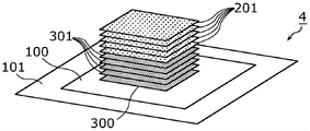
首先,利用图1对实施方式所涉及的AI芯片的概要进行说明。图1是示意性地示出本实施方式所涉及的AI芯片1的透视图。First, the outline of the AI chip according to the embodiment will be described using FIG. 1 . FIG. 1 is a perspective view schematically showing an AI chip 1 according to this embodiment.
图1所示的AI芯片1是执行AI处理的半导体芯片。AI处理是用于利用人工智能的各种运算处理,例如用于自然语言处理、声音识别处理、图像识别处理和推荐、以及各种设备的控制处理等。AI处理例如包括机器学习或深度学习等。The AI chip 1 shown in FIG. 1 is a semiconductor chip that performs AI processing. AI processing is various arithmetic processing using artificial intelligence, such as natural language processing, voice recognition processing, image recognition processing and recommendation, and control processing of various devices. AI processing includes, for example, machine learning or deep learning, among others.
如图1所示,AI芯片1具备系统芯片100、封装衬底101、存储数据的多个存储器裸片201、以及进行AI处理中包括的运算的多个运算裸片301。系统芯片100被安装在封装衬底101。多个存储器裸片201以及多个运算裸片301被安装在系统芯片100。多个存储器裸片201以及多个运算裸片301分别是裸芯片。As shown in FIG. 1 , the AI chip 1 includes a
在本实施方式中,系统芯片100具备存储数据的存储器裸片200、以及进行AI处理中包括的运算的运算裸片300。因此,系统芯片100能够单独(也就是说,可以不层叠存储器裸片201以及运算裸片301)执行AI处理。为了使AI处理高速化,而追加设置存储器裸片201以及运算裸片301。为了提高存储容量以及运算能力,存储器裸片201以及运算裸片301分别设置所需要的个数。In the present embodiment, the
多个存储器裸片201被层叠在存储器裸片200的上方。存储器裸片201的个数越多,则越能够增加能够用于AI处理的存储容量。按照AI芯片1需要的存储容量来决定存储器裸片201的个数。AI芯片1至少具备一个存储器裸片201。存储容量与存储器裸片的个数成比例地增长。A plurality of memory die 201 is stacked above memory die 200 . As the number of memory dies 201 increases, the memory capacity that can be used for AI processing can be increased. The number of memory dies 201 is determined according to the storage capacity required by the AI chip 1 . The AI chip 1 includes at least one memory die 201 . Storage capacity grows proportionally to the number of memory dies.
多个运算裸片301被层叠在运算裸片300的上方。运算裸片301的个数越多,则越能够提高能够用于AI处理的运算能力。按照AI芯片1所需要的运算能力来决定运算裸片301的个数。AI芯片1至少具备一个运算裸片301。A plurality of computing die 301 is stacked on top of computing die 300 . The greater the number of computing dies 301 , the more computing power available for AI processing can be improved. The number of computing dies 301 is determined according to the computing capability required by the AI chip 1 . The AI chip 1 has at least one computing die 301 .
运算能力例如是每单位时间能够执行的指令数(TOPS:Tera Operations PerSecond)。例如,一个运算裸片301具有消耗1W的电力来执行40TOPS的指令执行能力。如图1所示,由于层叠有包括运算裸片300在内的共计七个运算裸片,因此,AI芯片1具有消耗7W的电力来执行280TOPS的指令执行能力。如此,AI芯片1的处理能力与运算裸片的个数成比例地增长。The computing power is, for example, the number of instructions that can be executed per unit time (TOPS: Tera Operations Per Second). For example, one computing die 301 has an instruction execution capability of 40 TOPS while consuming 1W of power. As shown in FIG. 1 , since a total of seven arithmetic dies including the arithmetic die 300 are stacked, the AI chip 1 has an instruction execution capability of 280 TOPS by consuming 7W of power. In this way, the processing capability of the AI chip 1 increases in proportion to the number of computing chips.
在本实施方式中,存储器裸片与运算裸片被分开层叠。也就是说,在系统芯片100的平面图中,多个存储器裸片以及多个运算裸片被配置在互不相同的区域。In this embodiment, memory dies and computing dies are stacked separately. That is, in the plan view of the
具体而言,如图1所示,系统芯片100具有第1区域102以及第2区域103。在平面图中,第1区域102是与第2区域103不同的区域。Specifically, as shown in FIG. 1 , the
存储器裸片200以及多个存储器裸片201被配置在第1区域102。具体而言,存储器裸片200被配置在第1区域102,所有的存储器裸片201被层叠在存储器裸片200上。在平面图中,存储器裸片200和所有的存储器裸片201彼此重叠。在一个存储器裸片200或201上就会层叠一个存储器裸片201。The memory die 200 and the plurality of memory die 201 are arranged in the
运算裸片300以及多个运算裸片301被配置在第2区域103。具体而言,运算裸片300被配置在第2区域103,所有的运算裸片301被层叠在运算裸片300上。在平面图中,运算裸片300和所有的运算裸片301彼此重叠。在一个运算裸片300或301上就会层叠一个运算裸片301。The arithmetic die 300 and the plurality of arithmetic die 301 are arranged in the
如上所述,AI芯片1被构成为,能够根据需要的个数来分别层叠存储器裸片以及运算裸片。也就是说,在需要存储容量的情况下,能够层叠所需要的个数的运算裸片201。在需要存储容量的情况下,能够层叠所需要的个数的运算裸片301。在需要存储容量以及运算能力这两者的情况下,能够层叠所需要的个数的存储器裸片201以及所需要的个数的运算裸片301。这样,能够以可扩展的方式简单地变更AI芯片1的性能。因此,能够简单地提高AI芯片1的处理能力。As described above, the AI chip 1 is configured such that memory dies and arithmetic dies can be separately stacked according to the required number. That is, when the storage capacity is required, a required number of arithmetic dies 201 can be stacked. When storage capacity is required, a required number of arithmetic dies 301 can be stacked. When both the storage capacity and the computing power are required, a required number of memory dies 201 and a required number of computing dies 301 can be stacked. In this way, the performance of the AI chip 1 can be easily changed in a scalable manner. Therefore, the processing capability of the AI chip 1 can be easily increased.
[2.构成][2. Composition]
接着,对AI芯片1的各构成要素的具体构成进行说明。Next, a specific configuration of each component of the AI chip 1 will be described.
[2-1.系统芯片][2-1. System on Chip]
首先,利用图2对系统芯片100的构成进行说明。图2是示出本实施方式所涉及的AI芯片1具备的系统芯片100的构成的方框图。First, the configuration of the
系统芯片100对整个AI芯片1进行控制。具体而言,系统芯片100对多个存储器裸片200和201以及多个运算裸片300和301进行控制。The
如图2所示,系统芯片100具备微控制器110、系统总线120、外部接口130、图像处理引擎140、DRAM(Dynamic RandomAccess Memory:动态随机存取存储器)控制器150、以及AI加速器160。As shown in FIG. 2 , the
微控制器110是对系统芯片100全体进行控制的控制块的一个例子。微控制器110经由系统总线120,与外部接口130、图像处理引擎140、DRAM控制器150以及AI加速器160分别进行数据以及信息的收发,并且执行运算以及指令。如图2所示,微控制器110具备多个CPU(Central Processing Unit:中央处理器)111、以及二级高速缓存112。另外,微控制器110具备的CPU111的个数也可以仅是一个。并且,微控制器110也可以不具备二级高速缓存112。The
微控制器110使从存储器裸片200以及多个存储器裸片201中选择的任意的存储器裸片存储AI处理所需要的数据。也就是说,能够存储在一个存储器裸片200或201中的数据也能够被存储到其他的存储器裸片200或201。微控制器110将层叠的所有的存储器裸片201作为有效存储区来利用。在新的存储器裸片201被层叠的情况下,微控制器110能够对新的存储器裸片201进行与现有的存储器裸片200或201同等的控制。The
并且,微控制器110使从运算裸片300以及多个运算裸片301中选择的任意的运算裸片执行AI处理中包括的运算。也就是说,一个运算裸片300或301能够执行的指令在其他的运算裸片300或301中也能够被执行。微控制器110将层叠的所有的运算裸片301作为有效运算电路来利用。在新的运算裸片301被层叠的情况下,微控制器110能够对新的运算裸片301进行与现有的运算裸片300或301同等的控制。Then, the
系统总线120是用于收发数据以及信号等的布线。系统总线120与微控制器110、外部接口130、图像处理引擎140、DRAM控制器150以及AI加速器160电连接,能够彼此通信。The
外部接口130是用于与不同于AI芯片1的外部装置进行数据以及信号的收发的接口。The
图像处理引擎140是对图像信号或影像信号进行处理的信号处理电路。例如,图像处理引擎140执行画质调整处理等。The
DRAM控制器150是对与AI芯片1不同的外部存储器进行数据的读出以及写入等的存储控制器。The
AI加速器160是高速进行AI处理的信号处理电路。如图2所示,AI加速器160具备内部总线161、存储器裸片200、运算裸片300、以及DSP(Digital Signal Processor:数字信号处理器)400。The
内部总线161是用于收发AI加速器160内的数据以及信号等的布线。内部总线161与存储器裸片200、运算裸片300以及DSP400电连接,能够彼此通信。内部总线161也用于对多个存储器裸片201以及多个运算裸片301进行数据以及信号等的收发。内部总线161和系统总线120构成了对微控制器110与多个存储器裸片200和201、以及多个运算裸片300和301进行电连接的总线。The
存储器裸片200是AI芯片1具备的多个存储器裸片的其中之一的第1存储器裸片的一个例子。如图3所示,在存储器裸片200具有的布局图案(第1布局图案)的上方层叠有多个存储器裸片201。在此,图3是示意性地示出图2所示的方框图与图1所示的透视图的关系的图。多个存储器裸片201分别是被层叠在第1存储器裸片具有的第1布局图案的上方的第2存储器裸片的一个例子。The memory die 200 is an example of a first memory die among the plurality of memory dies included in the AI chip 1 . As shown in FIG. 3 , a plurality of memory dies 201 are stacked above the layout pattern (first layout pattern) of the memory die 200 . Here, FIG. 3 is a diagram schematically showing the relationship between the block diagram shown in FIG. 2 and the perspective view shown in FIG. 1 . Each of the plurality of memory dies 201 is an example of a second memory die stacked on the first layout pattern of the first memory die.
运算裸片300是AI芯片1具备的多个运算裸片的其中之一的第1运算裸片的一个例子。如图3所示,在运算裸片300具有的布局图案(第2布局图案)的上方层叠有多个运算裸片301。多个运算裸片301分别是被层叠在第1运算裸片具有的第2布局图案的上方的第2运算裸片的一个例子。The computation die 300 is an example of a first computation die among the plurality of computation dies included in the AI chip 1 . As shown in FIG. 3 , a plurality of arithmetic dies 301 are stacked above the layout pattern (second layout pattern) of the
DSP400是进行与AI处理有关的数字信号处理的处理器。DSP400 is a processor that performs digital signal processing related to AI processing.
另外,系统芯片100的构成,并非受图2所示的例子所限。例如,系统芯片100也可以不具备图像处理引擎140。系统芯片100也可以具备专用于规定的处理的信号处理电路等。In addition, the configuration of the
[2-2.存储器裸片][2-2. Memory Die]
接着,利用图4对存储器裸片200以及201的构成进行说明。图4是示出本实施方式所涉及的AI芯片1具备的存储器裸片200以及201的平面布局的一个例子的平面图。Next, configurations of the memory dies 200 and 201 will be described using FIG. 4 . FIG. 4 is a plan view showing an example of the planar layout of the memory dies 200 and 201 included in the AI chip 1 according to the present embodiment.
存储器裸片200和多个存储器裸片201分别具有相同的布局图案。具体而言,存储器裸片200和多个存储器裸片201分别具有相同的构成,各自的存储容量相同。以下,以存储器裸片201的构成为中心进行说明。The memory die 200 and the plurality of memory dies 201 respectively have the same layout pattern. Specifically, the memory die 200 and the plurality of memory dies 201 each have the same configuration and have the same memory capacity. The following description focuses on the configuration of the memory die 201 .
存储器裸片201例如是DRAM或SRAM等易失性存储器。存储器裸片201也可以是NAND型闪存等非易失性存储器。如图4所示,存储器裸片201具备一个以上的存储器块210、一个以上的输入输出端口240、以及一个以上的布线260。一个以上的存储器块210、一个以上的输入输出端口240、以及一个以上的布线260分别被形成在构成存储器裸片201的硅衬底的表面或内部。存储器裸片201的布局图案由存储器块210、输入输出端口240以及布线260各自的大小、形状、个数以及配置等来表示。The memory die 201 is, for example, a volatile memory such as DRAM or SRAM. The memory die 201 may also be a non-volatile memory such as NAND flash memory. As shown in FIG. 4 , the memory die 201 includes one or more memory blocks 210 , one or more input/
一个以上的存储器块210分别是包括一个以上的存储单元且存储数据的存储电路。在图4所示的例子中,在一个以上的存储器块210中虽然包括面积(存储容量)不同的存储器块,但也可以是所有的存储器块210的面积相同。Each of the one or more memory blocks 210 is a memory circuit including one or more memory cells and storing data. In the example shown in FIG. 4 , one or more memory blocks 210 include memory blocks with different areas (storage capacities), but all the memory blocks 210 may have the same area.
一个以上的输入输出端口240分别是对存储器裸片201进行数据以及信号的输入输出的端子。存储器裸片201经由输入输出端口240,与上下层叠的存储器裸片200或201电连接。存储器裸片201与存储器裸片200电连接,并且经由存储器裸片200,与内部总线161以及系统总线120电连接。在图4所示的例子中,一个以上的输入输出端口240被配置为沿着存储器裸片201的外周而呈环状,但并非受此所限。例如,一个以上的输入输出端口240也可以被设置在存储器裸片201的中央。The one or more input/
一个以上的布线260是对输入输出端口240与存储器块210进行连接的电布线,用于数据的收发。一个以上的布线260例如包括位线以及字线。在图4所示的例子中,一个以上的布线260被设置为格子状,但也可以是条纹状。The one or
在图4中虽然对存储器裸片200以及201的构成的一个例子进行了简单地示意,但是只要布局图案相同,存储器裸片200以及201的构成就没有特殊的限定。Although an example of the configuration of the memory dies 200 and 201 is briefly shown in FIG. 4 , the configurations of the memory dies 200 and 201 are not particularly limited as long as the layout patterns are the same.
[2-3.运算裸片][2-3. Computing die]
接着,利用图5对运算裸片300以及301的构成进行说明。图5是示出本实施方式所涉及的AI芯片1具备的运算裸片300以及301的平面布局的一个例子的平面图。Next, configurations of the arithmetic dies 300 and 301 will be described using FIG. 5 . FIG. 5 is a plan view showing an example of the planar layout of the arithmetic dies 300 and 301 included in the AI chip 1 according to the present embodiment.
运算裸片300与多个运算裸片301分别具有相同的布局图案。具体而言,运算裸片300与多个运算裸片301分别具有相同的构成,各自的运算能力相同。以下,以运算裸片301的构成为中心进行说明。The computing die 300 and the plurality of computing dies 301 respectively have the same layout pattern. Specifically, the
运算裸片301具有可重写电路。具体而言,运算裸片301是FPGA(FieldProgrammable GateArray:现场可编程门阵列)。如图5所示,运算裸片301具备一个以上的AI处理块310、一个以上的逻辑块320、一个以上的开关块330、一个以上的输入输出端口340、一个以上的连接块350、以及一个以上的布线360。一个以上的AI处理块310、一个以上的逻辑块320、一个以上的开关块330、一个以上的输入输出端口340、一个以上的连接块350、以及一个以上的布线360被形成在构成运算裸片301的硅衬底的表面或内部。运算裸片301的布局图案由AI处理块310、逻辑块320、开关块330、输入输出端口340、连接块350以及布线360各自的大小、形状、个数以及配置来表示。The arithmetic die 301 has rewritable circuitry. Specifically, the
一个以上的AI处理块310分别是用于AI处理的加速器电路。对于AI处理块310的具体构成,以后将利用图6进行说明。The one or more AI processing blocks 310 are respectively accelerator circuits for AI processing. The specific configuration of the
一个以上的逻辑块320分别是进行逻辑运算的运算电路。一个以上的AI处理块310以及一个以上的逻辑块320被排列配置成矩阵状。例如,在图5所示的例子中,一个以上的AI处理块310以及一个以上的逻辑块320被排列配置成3行×3列,各块经由开关块330以及连接块350通过布线360电连接。另外,AI处理块310的个数也可以仅是一个,没有特殊的限定。并且,一个以上的AI处理块310以及一个以上的逻辑块320的配置,并不限于是矩阵状,也可以是条纹状。The one or more logic blocks 320 are arithmetic circuits for performing logic operations. One or more AI processing blocks 310 and one or more logic blocks 320 are arranged in a matrix. For example, in the example shown in FIG. 5 , more than one
一个以上的开关块330分别是对与开关块330相邻的2个至4个连接块350的连接关系进行切换的切换电路。Each of the one or more switch blocks 330 is a switching circuit for switching the connection relationship between two to four
一个以上的输入输出端口340分别是对运算裸片301进行数据以及信号的输入输出的端子。运算裸片301经由输入输出端口340,与上下层叠的运算裸片300或301连接。运算裸片301与运算裸片300连接,并且经由运算裸片300,与内部总线161以及系统总线120连接。在图5所示的例子中,一个以上的输入输出端口340被配置为沿着运算裸片301的外周而呈环状,但并非受此所限。例如,一个以上的输入输出端口340也可以被设置在运算裸片301的中央。The one or more input/
一个以上的连接块350分别是用于对与连接块350相邻的AI处理块310、逻辑块320以及开关块330进行连接的电路。The one or more connection blocks 350 are circuits for connecting the
一个以上的布线360是将输入输出端口340与AI处理块310以及逻辑块320等连接的电布线,用于数据的收发。在图5所示的例子中,一个以上的布线360被设置为格子状,但也可以是条纹状。The one or
在开关块330以及连接块350中,输入输出端口340、AI处理块310以及逻辑块320的连接关系被切换,从而运算裸片301能够进行特定的运算处理。开关块330以及连接块350的切换,例如利用未图示的存储器中存储的构成信息(配置数据)来进行。In the
接着,利用图6对AI处理块310的具体构成进行说明。图6是示出本实施方式所涉及的运算裸片300以及301具备的AI处理块310的构成的方框图。Next, a specific configuration of the
AI处理块310进行AI处理中包括的运算。具体而言,AI处理块310至少进行卷积运算、矩阵运算以及池化运算的其中之一。如图6所示,AI处理块310例如包括对数处理电路311。对数处理电路311进行对数量化后的输入数据的运算。具体而言,对数处理电路311进行对数量化后的输入数据的卷积运算。卷积运算中包括的乘法处理可以通过将运算对象的数据转换成对数域,从而能够以加法处理来执行。据此,实现AI处理的高速化。The
并且,AI处理块310进行的AI处理也可以包括利用了抖动的误差扩散法。具体而言,AI处理块310包括抖动电路312。抖动电路312进行利用了误差扩散法的运算。据此,即使位数少也能够抑制运算精度的劣化。Also, the AI processing performed by the
在图5中虽然对运算裸片300以及301的构成的一个例子进行了简单地示意,但是只要布局图案相同,运算裸片300以及301的构成就没有特殊的限定。Although an example of the configuration of the computing dies 300 and 301 is briefly shown in FIG. 5 , the configurations of the computing dies 300 and 301 are not particularly limited as long as the layout patterns are the same.
[3.层叠的裸片彼此的连接][3. Connection between stacked dies]
接着,对层叠的裸片彼此的连接进行说明。关于裸片彼此的连接,既有利用TSV(Through SiliconVia:硅穿孔)的情况,也有利用无线的情况。Next, connection between stacked dies will be described. As for the connection between bare chips, there are cases where TSV (Through Silicon Via: Through Silicon Via) is used, and there is a case where wireless is used.
[3-1.TSV][3-1.TSV]
图7是示出本实施方式所涉及的对多个存储器裸片201以及多个运算裸片301的连接利用TSV的例子的剖面图。图7示出了系统芯片100经由凸块电极180安装在封装衬底101的情况。另外,存储器裸片200以及运算裸片300与系统芯片100形成一体,在图7中以虚线以及阴影来示意性地表示设置有存储器裸片200以及运算裸片300的区域。在图8中也同样如此。7 is a cross-sectional view showing an example of using TSVs for connecting a plurality of memory dies 201 and a plurality of arithmetic dies 301 according to this embodiment. FIG. 7 shows a situation where the
如图7所示,在多个存储器裸片201分别设置有TSV270。TSV270是贯通存储器裸片201的贯通导体的一个例子。TSV270例如由铜(Cu)等金属材料形成。具体而言,在将存储器裸片201在厚度方向上贯通而形成贯通孔后,将绝缘膜覆盖贯通孔的内壁,然后,通过电解镀金法等以金属材料来填充贯通孔,由此能够形成TSV270。As shown in FIG. 7 ,
在图7中,在TSV270的至少一方的端部,由铜等金属材料形成凸块电极280,使在层叠方向上相邻的存储器裸片201的TSV270彼此电连接。另外,在层叠方向上相邻的存储器裸片201连接也可以不使用凸块电极280。In FIG. 7 , at least one end of the
在平面图中,TSV270以及凸块电极280被设置在与图4所示的输入输出端口240重叠的位置。在本实施方式中,存储器裸片200以及多个存储器裸片201具有相同的布局图案,因此,在层叠了各个存储器裸片的情况下,输入输出端口240的位置在平面图中是一致的。因此,通过在厚度方向上贯通存储器裸片201的TSV270,能够简单地使存储器裸片201彼此电连接。In plan view,
与存储器裸片201一样,在多个运算裸片301分别设置有TSV370。TSV370是贯通运算裸片301的贯通导体的一个例子。TSV370的材料以及形成方法与TSV270相同。Like the memory die 201 ,
在图7中,在TSV370的至少一方的端部,由铜等金属材料形成凸块电极380,使在层叠方向上相邻的运算裸片301的TSV370彼此电连接。另外,在层叠方向上相邻的运算裸片301连接也可以不使用凸块电极380。In FIG. 7 , bump
在平面图中,TSV370以及凸块电极380被设置在与图5所示的输入输出端口340重叠的位置。在本实施方式中,运算裸片300以及多个运算裸片301具有相同的布局图案,因此,在层叠了各个运算裸片的情况下,在平面图中输入输出端口340的位置一致。因此,通过在厚度方向上贯通运算裸片301的TSV370,能够简单地使运算裸片301彼此电连接。In plan view,
另外,为了使最上层的存储器裸片201与最下层的存储器裸片200电连接,而在除了最上层的存储器裸片201以外的所有的存储器裸片201分别设置有TSV270。同样,为了使从上往下的第2个存储器裸片201与存储器裸片200电连接,而在除了最上层以及从上往下的第2个存储器裸片201以外的所有的存储器裸片201分别设置有TSV270。此时,用于连接最上层的存储器裸片201的TSV270与用于连接从上往下的第2个存储器裸片201的TSV270,可以共用相同的TSV,也可以分别使用不同的TSV。运算裸片301也同样如此。In addition, in order to electrically connect the uppermost memory die 201 and the lowermost memory die 200 , all the memory die 201 except the uppermost memory die 201 are respectively provided with
[3-2.无线][3-2. Wireless]
图8是示出本实施方式所涉及的对多个存储器裸片201以及多个运算裸片301的连接利用无线的例子的剖面图。将利用了无线的连接也称为无线TSV技术。FIG. 8 is a cross-sectional view showing an example in which a plurality of
如图8所示,在多个存储器裸片201分别设置有无线通信电路290。无线通信电路290进行通信范围为几十μm左右的超近距离无线通信。具体而言,无线通信电路290具有微小的线圈,利用线圈间的磁场耦合来进行通信。As shown in FIG. 8 , a
与存储器裸片201一样,在多个运算裸片301分别设置有无线通信电路390。无线通信电路390进行通信范围为几十μm左右的超近距离无线通信。具体而言,无线通信电路390具有微小的线圈,利用线圈间的磁场耦合来进行通信。Like the memory die 201 , a
图8示出了无线通信电路290以及390的每一个被嵌入在衬底内的例子,但并非受此所限。无线通信电路290以及390也可以被设置在衬底的上表面以及下表面的至少一方。FIG. 8 shows an example in which
另外,对存储器裸片201的连接可以利用TSV,对运算裸片301的连接可以利用无线。或者,对存储器裸片201的连接可以利用无线,对运算裸片301的连接可以利用TSV。并且,对存储器裸片201的连接可以利用TSV以及无线这两者。同样,对运算裸片301的连接可以利用TSV以及无线这两者。In addition, the connection to the
[4.变形例][4. Modifications]
接着,对实施方式所涉及的AI芯片1的变形例进行说明。以下,以与上述的实施方式不同之处为中心进行说明,省略或简化共同点的说明。Next, a modification example of the AI chip 1 according to the embodiment will be described. Hereinafter, differences from the above-described embodiment will be mainly described, and descriptions of common points will be omitted or simplified.
[4-1.变形例1][4-1. Modification 1]
首先,对变形例1所涉及的AI芯片进行说明。在变形例1中,在存储器裸片以及运算裸片的至少一方的层叠中采用了中介层。First, the AI chip according to Modification 1 will be described. In Modification 1, an interposer is used for stacking at least one of the memory die and the arithmetic die.
图9是示意性地示出变形例1所涉及的AI芯片2的透视图。如图9所示,在AI芯片2中,系统芯片100具备中介层500。系统芯片100不具备存储器裸片200以及运算裸片300。FIG. 9 is a perspective view schematically showing an
中介层500是对芯片与衬底的电连接进行中继的中继部件。在本变形例中,多个存储器裸片201的其中之一、以及多个运算裸片301的其中之一分别被层叠在中介层500上。剩下的存储器裸片201被层叠在中介层500上层叠的存储器裸片201的上方。剩下的运算裸片301被层叠在中介层500上层叠的运算裸片301的上方。The
另外,在本变形例中,系统芯片100也可以具备存储器裸片200以及运算裸片300的一方。换而言之,也可以仅将存储器裸片以及运算裸片的任意一方层叠在中介层500上。In addition, in this modified example, the
例如,AI芯片2也可以具备被层叠在系统芯片100具备的存储器裸片200的上方的一个以上的存储器裸片201、以及被层叠在中介层500上的多个运算裸片301。或者,AI芯片2也可以具备被层叠在系统芯片100具备的运算裸片300的上方的一个以上的运算裸片301、以及被层叠在中介层500上的多个存储器裸片201。For example, the
[4-2.变形例2][4-2. Modification 2]
接着,对变形例2所涉及的AI芯片进行说明。在变形例2中,存储器裸片以及运算裸片被混在一起层叠。Next, the AI chip according to
图10至图13分别是示意性地示出变形例2所涉及的AI芯片3至6的透视图。10 to 13 are perspective views schematically showing
在图10所示的AI芯片3中,系统芯片100具备存储器裸片200,而不具备运算裸片300。在存储器裸片200的上方依次层叠多个存储器裸片201以及多个运算裸片301。也就是说,在多个存储器裸片201中的最上层的存储器裸片201上层叠有多个运算裸片301中的最下层的运算裸片301。In the
另外,如图11所示的AI芯片4,也可以在多个运算裸片301的上方层叠有多个存储器裸片201。在AI芯片4中,系统芯片100具备运算裸片300,而不具备存储器裸片200。在运算裸片300的上方依次层叠多个运算裸片301以及多个存储器裸片201。也就是说,在多个运算裸片301中的最上层的运算裸片301上层叠有多个存储器裸片201中的最下层的存储器裸片201。In addition, in the AI chip 4 shown in FIG. 11 , a plurality of memory dies 201 may be stacked on top of a plurality of computing dies 301 . In the AI chip 4 , the
或者,也可以像图12所示的AI芯片5那样,交替层叠存储器裸片201与运算裸片301。在AI芯片5中,系统芯片100具备存储器裸片200,而不具备运算裸片300。在存储器裸片200上,一个运算裸片301与一个存储器裸片201交替地层叠。另外,在AI芯片5中,系统芯片100也可以具备运算裸片300,而不具备存储器裸片200。在运算裸片300上,也可以一个存储器裸片201与一个运算裸片301交替地层叠。并且,在AI芯片5中,系统芯片100也可以具备存储器裸片200以及运算裸片300。也可以在存储器裸片200以及运算裸片300各自的上方,一个存储器裸片201与一个运算裸片301交替地层叠。并且,存储器裸片201以及运算裸片301的至少一方也可以一次层叠多个。Alternatively, like the
并且,如图13所示的AI芯片6,也可以在中介层500上层叠存储器裸片201以及运算裸片301。在AI芯片6中,系统芯片100不具备存储器裸片200以及运算裸片300,而具备中介层500。在中介层500上层叠有多个运算裸片301的其中之一。在被层叠在中介层500上的运算裸片301的上方层叠有剩下的运算裸片301以及存储器裸片201。另外,在中介层500上也可以层叠存储器裸片201。并且,层叠在中介层500的上方的存储器裸片201与运算裸片301,可以一个与一个交替层叠,也可以多个与多个交替层叠。Furthermore, in the AI chip 6 shown in FIG. 13 , the memory die 201 and the arithmetic die 301 may be stacked on the
如上所述,对存储器裸片与运算裸片的层叠方法并没有特别的限定,从而实现设计变更自由度高的AI芯片。As described above, there is no particular limitation on the stacking method of the memory die and the computing die, thereby realizing an AI chip with a high degree of freedom in design changes.
(其他实施方式)(Other implementations)
以上,对1个或多个形态所涉及的AI芯片,根据实施方式进行了说明,但是,本公开并不受这些实施方式所限。只要不脱离本公开的主旨,对本实施方式执行本领域技术人员想到的各种变形的形态,或组合不同的实施方式的构成要素来构成的形态,也可以包含在本公开的范围内。As above, the AI chip according to one or more aspects has been described based on the embodiments, but the present disclosure is not limited by these embodiments. As long as it does not deviate from the gist of the present disclosure, various modifications to this embodiment that can be thought of by those skilled in the art, or combinations of components of different embodiments are also included in the scope of the present disclosure.
例如,像图12所示的AI芯片5那样,也可以不将1个存储器裸片直接层叠在其他的存储器裸片的第1布局图案上。也就是说,位于上层的存储器裸片被层叠在位于下层的存储器裸片的布局图案的上方即可,在两者之间也可以存在运算裸片。同样,也可以不将1个运算裸片直接层叠在其他的运算裸片的第2布局图案上。也就是说,位于上层的运算裸片被层叠在位于下层的运算裸片的布局图案的上方即可,在两者之间也可以存在存储器裸片。另外,存储器裸片与存储器裸片之间、运算裸片与运算裸片之间、或存储器裸片与运算裸片之间不经由中介层而层叠。For example, like the
并且,运算裸片300以及301也可以是不能重写的电路。运算裸片300以及301至少具备一个AI处理块310即可,也可以不具备逻辑块320、开关块330以及连接块350。Also, the computing dies 300 and 301 may be non-rewritable circuits. The computing chips 300 and 301 need only include at least one
并且,对于上述的各实施方式,能够在技术方案或与其等通的范围内进行各种变更、替换、添加、省略等。In addition, various changes, substitutions, additions, omissions, etc. can be made to the above-mentioned embodiments within the scope of the technical claims or the like.
本公开能够用作能够简单地提高处理能力的AI芯片,例如能够用于各种电器产品以及计算机设备等。The present disclosure can be used as an AI chip that can easily improve processing capabilities, and can be used, for example, in various electrical products, computer equipment, and the like.
符号说明Symbol Description
1,2,3,4,5,6 AI芯片1, 2, 3, 4, 5, 6 AI chips
100 系统芯片100 SoCs
101 封装衬底101 Package Substrate
102 第1区域102 Area 1
103 第2区域103
110 微控制器110 Microcontrollers
111 CPU111 CPUs
112 二级高速缓存112 L2 cache
120 系统总线120 system bus
130 外部接口130 external interface
140 图像处理引擎140 image processing engine
150 DRAM控制器150 DRAM controllers
160 AI加速器160 AI accelerator
161 内部总线161 internal bus
180,280,380 凸块电极180, 280, 380 bump electrodes
200,201 存储器裸片200, 201 memory die
210 存储器块210 memory blocks
240,340 输入输出端口240, 340 input and output ports
260,360 布线260, 360 wiring
270,370 TSV270, 370 TSVs
290,390 无线通信电路290, 390 wireless communication circuit
300,301 运算裸片300, 301 computing die
310 AI处理块310 AI processing blocks
311 对数处理电路311 logarithmic processing circuit
312 抖动电路312 dither circuit
320 逻辑块320 logic blocks
330 开关块330 switch block
350 连接块350 connection block
400 DSP(数字信号处理器)400 DSP (Digital Signal Processor)
500 中介层500 interposers
Claims (16)
Applications Claiming Priority (3)
| Application Number | Priority Date | Filing Date | Title |
|---|---|---|---|
| JP2020093022 | 2020-05-28 | ||
| JP2020-093022 | 2020-05-28 | ||
| PCT/JP2021/015475 WO2021241048A1 (en) | 2020-05-28 | 2021-04-14 | Ai chip |
Publications (1)
| Publication Number | Publication Date |
|---|---|
| CN115516628A true CN115516628A (en) | 2022-12-23 |
Family
ID=78744363
Family Applications (1)
| Application Number | Title | Priority Date | Filing Date |
|---|---|---|---|
| CN202180029687.XA Pending CN115516628A (en) | 2020-05-28 | 2021-04-14 | AI chip |
Country Status (4)
| Country | Link |
|---|---|
| US (1) | US20230197711A1 (en) |
| JP (1) | JP7270234B2 (en) |
| CN (1) | CN115516628A (en) |
| WO (1) | WO2021241048A1 (en) |
Cited By (1)
| Publication number | Priority date | Publication date | Assignee | Title |
|---|---|---|---|---|
| CN117915670A (en) * | 2024-03-14 | 2024-04-19 | 上海芯高峰微电子有限公司 | Integrated chip structure for memory and calculation |
Families Citing this family (4)
| Publication number | Priority date | Publication date | Assignee | Title |
|---|---|---|---|---|
| KR20230057648A (en) * | 2021-10-22 | 2023-05-02 | 삼성전자주식회사 | Semiconductor device, semiconductor package, and method of fabricating semiconductor package |
| US12469820B2 (en) * | 2021-12-10 | 2025-11-11 | Intel Corporation | Fine-grained disaggregated server architecture |
| KR20240012139A (en) * | 2022-07-20 | 2024-01-29 | 삼성전자주식회사 | Semiconductor chip stack structure, semiconductor package and manufacturing method thereof |
| WO2025226352A1 (en) * | 2024-04-25 | 2025-10-30 | Qualcomm Incorporated | Single hybrid system-on-chip (soc) die structure with high memory bandwidth and density |
Citations (5)
| Publication number | Priority date | Publication date | Assignee | Title |
|---|---|---|---|---|
| US20100078790A1 (en) * | 2008-09-29 | 2010-04-01 | Hitachi, Ltd. | Semiconductor device |
| US20190050040A1 (en) * | 2018-09-28 | 2019-02-14 | Intel Corporation | Multi-die stacks with power management |
| US20190051642A1 (en) * | 2018-09-28 | 2019-02-14 | Intel Corporation | Multi-die packages with efficient memory storage |
| CN109388595A (en) * | 2017-08-10 | 2019-02-26 | 三星电子株式会社 | High-bandwidth memory systems and logic dice |
| CN109560078A (en) * | 2017-09-27 | 2019-04-02 | 三星电子株式会社 | Stacked storage device, storage system and operating method including it |
Family Cites Families (13)
| Publication number | Priority date | Publication date | Assignee | Title |
|---|---|---|---|---|
| US7064579B2 (en) * | 2002-07-08 | 2006-06-20 | Viciciv Technology | Alterable application specific integrated circuit (ASIC) |
| JP4549418B2 (en) * | 2008-03-04 | 2010-09-22 | シャープ株式会社 | Image processing apparatus, image processing method, image forming apparatus, program, and recording medium |
| US20140013129A1 (en) * | 2012-07-09 | 2014-01-09 | L. Pierre de Rochemont | Hybrid computing module |
| JP5970078B2 (en) | 2011-12-02 | 2016-08-17 | インテル・コーポレーション | Stacked memory that enables device interconnect changes |
| US9093756B2 (en) * | 2012-09-18 | 2015-07-28 | Panasonic Intellectual Property Management Co., Ltd. | Antenna, transmitter device, receiver device, three-dimensional integrated circuit, and contactless communication system |
| US10460747B2 (en) * | 2016-05-10 | 2019-10-29 | Google Llc | Frequency based audio analysis using neural networks |
| US11609623B2 (en) * | 2017-09-01 | 2023-03-21 | Qualcomm Incorporated | Ultra-low power neuromorphic artificial intelligence computing accelerator |
| US10840240B2 (en) * | 2018-10-24 | 2020-11-17 | Micron Technology, Inc. | Functional blocks implemented by 3D stacked integrated circuit |
| US10903153B2 (en) | 2018-11-18 | 2021-01-26 | International Business Machines Corporation | Thinned die stack |
| US12424515B2 (en) | 2018-11-28 | 2025-09-23 | Taiwan Semiconductor Manufacturing Co., Ltd. | SOIC chip architecture |
| US11100193B2 (en) * | 2018-12-07 | 2021-08-24 | Samsung Electronics Co., Ltd. | Dataflow accelerator architecture for general matrix-matrix multiplication and tensor computation in deep learning |
| US20200249996A1 (en) * | 2019-02-04 | 2020-08-06 | Pathtronic Inc. | Systems and methods for artificial intelligence hardware processing |
| US11171115B2 (en) * | 2019-03-18 | 2021-11-09 | Kepler Computing Inc. | Artificial intelligence processor with three-dimensional stacked memory |
-
2021
- 2021-04-14 CN CN202180029687.XA patent/CN115516628A/en active Pending
- 2021-04-14 US US17/995,972 patent/US20230197711A1/en not_active Abandoned
- 2021-04-14 JP JP2022527567A patent/JP7270234B2/en active Active
- 2021-04-14 WO PCT/JP2021/015475 patent/WO2021241048A1/en not_active Ceased
Patent Citations (5)
| Publication number | Priority date | Publication date | Assignee | Title |
|---|---|---|---|---|
| US20100078790A1 (en) * | 2008-09-29 | 2010-04-01 | Hitachi, Ltd. | Semiconductor device |
| CN109388595A (en) * | 2017-08-10 | 2019-02-26 | 三星电子株式会社 | High-bandwidth memory systems and logic dice |
| CN109560078A (en) * | 2017-09-27 | 2019-04-02 | 三星电子株式会社 | Stacked storage device, storage system and operating method including it |
| US20190050040A1 (en) * | 2018-09-28 | 2019-02-14 | Intel Corporation | Multi-die stacks with power management |
| US20190051642A1 (en) * | 2018-09-28 | 2019-02-14 | Intel Corporation | Multi-die packages with efficient memory storage |
Cited By (2)
| Publication number | Priority date | Publication date | Assignee | Title |
|---|---|---|---|---|
| CN117915670A (en) * | 2024-03-14 | 2024-04-19 | 上海芯高峰微电子有限公司 | Integrated chip structure for memory and calculation |
| CN117915670B (en) * | 2024-03-14 | 2024-07-05 | 上海芯高峰微电子有限公司 | Integrated chip structure for memory and calculation |
Also Published As
| Publication number | Publication date |
|---|---|
| JPWO2021241048A1 (en) | 2021-12-02 |
| JP7270234B2 (en) | 2023-05-10 |
| WO2021241048A1 (en) | 2021-12-02 |
| US20230197711A1 (en) | 2023-06-22 |
Similar Documents
| Publication | Publication Date | Title |
|---|---|---|
| CN115516628A (en) | AI chip | |
| US9748201B2 (en) | Semiconductor packages including an interposer | |
| US11004477B2 (en) | Bank and channel structure of stacked semiconductor device | |
| US20170179078A1 (en) | Semiconductor packages and methods of manufacturing the same | |
| CN115132698B (en) | Semiconductor devices including through-hole structures | |
| CN121908560A (en) | 3D computing circuit with high density Z-axis interconnect | |
| US20150091188A1 (en) | Semiconductor device having dummy cell array | |
| TW202011558A (en) | Stack packages including bridge dies | |
| US9275688B2 (en) | Semiconductor device and semiconductor package | |
| CN108074912A (en) | Semiconductor packages including connectors | |
| US9922965B2 (en) | Manufacturing methods semiconductor packages including through mold connectors | |
| CN112786565A (en) | Package-on-package with interposer bridge | |
| CN112018102A (en) | semiconductor package | |
| US11417642B2 (en) | Semiconductor storage device | |
| US20190363049A1 (en) | Multiple die package using an embedded bridge connecting dies | |
| CN110416174A (en) | Including the stacked package through molding through-hole | |
| CN113113386A (en) | Semiconductor package including stacked modules with interposer bridge | |
| US11322475B2 (en) | Stack semiconductor packages having wire-bonding connection structure | |
| US20120049361A1 (en) | Semiconductor integrated circuit | |
| US9824954B2 (en) | Semiconductor package comprising stacked integrated circuit chips having connection terminals and through electrodes symmetrically arranged | |
| CN114400209B (en) | Interposer, semiconductor packaging device and electronic device | |
| CN113257787B (en) | Semiconductor package including chips stacked on a base module | |
| WO2011107612A1 (en) | Customizable interconnections between electronic circuits | |
| WO2022029825A1 (en) | Computation circuit and ai processing module | |
| WO2022172609A1 (en) | Ai module |
Legal Events
| Date | Code | Title | Description |
|---|---|---|---|
| PB01 | Publication | ||
| PB01 | Publication | ||
| SE01 | Entry into force of request for substantive examination | ||
| SE01 | Entry into force of request for substantive examination | ||
| WD01 | Invention patent application deemed withdrawn after publication | ||
| WD01 | Invention patent application deemed withdrawn after publication |
Application publication date: 20221223 |