CN115507948A - Optical filter of spectrometer, manufacturing method and spectrum reconstruction method - Google Patents
Optical filter of spectrometer, manufacturing method and spectrum reconstruction method Download PDFInfo
- Publication number
- CN115507948A CN115507948A CN202210621430.XA CN202210621430A CN115507948A CN 115507948 A CN115507948 A CN 115507948A CN 202210621430 A CN202210621430 A CN 202210621430A CN 115507948 A CN115507948 A CN 115507948A
- Authority
- CN
- China
- Prior art keywords
- photonic crystal
- crystal plate
- silicon photonic
- spacer
- substrate
- Prior art date
- Legal status (The legal status is an assumption and is not a legal conclusion. Google has not performed a legal analysis and makes no representation as to the accuracy of the status listed.)
- Pending
Links
Images


Classifications
-
- G—PHYSICS
- G01—MEASURING; TESTING
- G01J—MEASUREMENT OF INTENSITY, VELOCITY, SPECTRAL CONTENT, POLARISATION, PHASE OR PULSE CHARACTERISTICS OF INFRARED, VISIBLE OR ULTRAVIOLET LIGHT; COLORIMETRY; RADIATION PYROMETRY
- G01J3/00—Spectrometry; Spectrophotometry; Monochromators; Measuring colours
- G01J3/28—Investigating the spectrum
- G01J3/2803—Investigating the spectrum using photoelectric array detector
-
- G—PHYSICS
- G01—MEASURING; TESTING
- G01J—MEASUREMENT OF INTENSITY, VELOCITY, SPECTRAL CONTENT, POLARISATION, PHASE OR PULSE CHARACTERISTICS OF INFRARED, VISIBLE OR ULTRAVIOLET LIGHT; COLORIMETRY; RADIATION PYROMETRY
- G01J3/00—Spectrometry; Spectrophotometry; Monochromators; Measuring colours
- G01J3/02—Details
- G01J3/0205—Optical elements not provided otherwise, e.g. optical manifolds, diffusers, windows
-
- G—PHYSICS
- G01—MEASURING; TESTING
- G01J—MEASUREMENT OF INTENSITY, VELOCITY, SPECTRAL CONTENT, POLARISATION, PHASE OR PULSE CHARACTERISTICS OF INFRARED, VISIBLE OR ULTRAVIOLET LIGHT; COLORIMETRY; RADIATION PYROMETRY
- G01J3/00—Spectrometry; Spectrophotometry; Monochromators; Measuring colours
- G01J3/02—Details
- G01J3/0256—Compact construction
- G01J3/0259—Monolithic
-
- G—PHYSICS
- G01—MEASURING; TESTING
- G01J—MEASUREMENT OF INTENSITY, VELOCITY, SPECTRAL CONTENT, POLARISATION, PHASE OR PULSE CHARACTERISTICS OF INFRARED, VISIBLE OR ULTRAVIOLET LIGHT; COLORIMETRY; RADIATION PYROMETRY
- G01J3/00—Spectrometry; Spectrophotometry; Monochromators; Measuring colours
- G01J3/28—Investigating the spectrum
- G01J3/2803—Investigating the spectrum using photoelectric array detector
- G01J2003/282—Modified CCD or like
Landscapes
- Physics & Mathematics (AREA)
- Spectroscopy & Molecular Physics (AREA)
- General Physics & Mathematics (AREA)
- Spectrometry And Color Measurement (AREA)
- Optical Filters (AREA)
Abstract
本申请提供的一种光谱仪滤光片、制作及光谱重建方法,其滤光片包括:基板;底部硅光子晶体板和顶部硅光子晶体板,位于所述基板一侧;间隔物,位于底部硅光子晶体板和顶部硅光子晶体板之间;其中所述基板靠近底部硅光子晶体板的一侧,以及间隔物靠近所述顶部硅光子晶体板的一侧形成一图案,所述间隔物、所述底部硅光子晶体板和顶部硅光子晶体板形成一腔体,本申请从而避免微加工方法导致重复薄膜沉积引起的应力问题,同时通过转移印刷得到的滤光片可以通过改变驱动电压值对光谱的腔长位移进行调控,从而可以调控滤光片的光学性能参数,进行光谱重构时,无需大量像素提供光谱数据,仅需通过调压即可获得大量光谱信息。

The application provides a spectrometer filter, its production and spectral reconstruction method, the filter comprising: a substrate; a bottom silicon photonic crystal plate and a top silicon photonic crystal plate, located on one side of the substrate; a spacer, located on the bottom silicon photonic crystal plate Between the photonic crystal plate and the top silicon photonic crystal plate; wherein the side of the substrate close to the bottom silicon photonic crystal plate, and the side of the spacer close to the top silicon photonic crystal plate form a pattern, the spacer, the The bottom silicon photonic crystal plate and the top silicon photonic crystal plate form a cavity, so that the application avoids the stress problem caused by repeated thin film deposition caused by the microfabrication method, and at the same time, the optical filter obtained by transfer printing can change the spectrum by changing the driving voltage value The cavity length displacement can be adjusted, so that the optical performance parameters of the filter can be adjusted. When performing spectral reconstruction, a large number of pixels do not need to provide spectral data, and a large amount of spectral information can be obtained only by adjusting the voltage.
Description
技术领域technical field
本申请涉及光谱分析技术领域,具体涉及一种光谱仪滤光片、制作及光谱重建方法。The present application relates to the technical field of spectral analysis, in particular to a spectrometer filter, its production and its spectral reconstruction method.
背景技术Background technique
中红外范围的小型化光谱仪可以用于环境监测、生物传感和自由空间通信等领域,现有技术中小型化光谱仪主要是基于波长重建方法的计算光谱仪,其具有超紧凑的占地面积,然而,现有技术需要多个像素阵列,因此不可避免地增加了器件的复杂性和占用空间,存在诸多不足。Miniaturized spectrometers in the mid-infrared range can be used in fields such as environmental monitoring, biosensing, and free space communication. The prior art miniaturized spectrometers are mainly computational spectrometers based on wavelength reconstruction methods, which have an ultra-compact footprint. However, , the prior art requires multiple pixel arrays, which inevitably increases the complexity and occupied space of the device, and has many disadvantages.
发明内容Contents of the invention
本申请提供一种光谱仪滤光片、制作及光谱重建方法,旨在解决目前现有技术需要多个像素阵列,因此不可避免地增加了器件的复杂性和占用空间的问题。The present application provides a spectrometer filter, its production and its spectral reconstruction method, aiming to solve the problem that the current prior art requires multiple pixel arrays, which inevitably increases the complexity and space of the device.
本申请第一方面实施例提供一种光谱仪滤光片,包括:The embodiment of the first aspect of the present application provides a spectrometer filter, including:
基板;Substrate;
底部硅光子晶体板和顶部硅光子晶体板,位于所述基板一侧;a bottom silicon photonic crystal plate and a top silicon photonic crystal plate on one side of the substrate;
间隔物,位于底部硅光子晶体板和顶部硅光子晶体板之间;其中所述基板靠近底部硅光子晶体板的一侧,以及间隔物靠近所述顶部硅光子晶体板的一侧形成一图案,所述间隔物、所述底部硅光子晶体板和顶部硅光子晶体板形成一腔体。a spacer between the bottom silicon photonic crystal plate and the top silicon photonic crystal plate; wherein the side of the substrate close to the bottom silicon photonic crystal plate and the side of the spacer close to the top silicon photonic crystal plate form a pattern, The spacers, the bottom silicon photonic crystal plate and the top silicon photonic crystal plate form a cavity.
在优选的实施例中,所述底部硅光子晶体板和顶部硅光子晶体板上蚀刻有多个周期性孔洞。In a preferred embodiment, the bottom silicon photonic crystal plate and the top silicon photonic crystal plate are etched with a plurality of periodic holes.
在优选的实施例中,所述基板和所述间隔物上设置有电极。In a preferred embodiment, electrodes are disposed on the substrate and the spacer.
在优选的实施例中,还包括:In a preferred embodiment, it also includes:
电隔离层,设于所述间隔物和所述底部硅光子晶体板之间。An electrical isolation layer is disposed between the spacer and the bottom silicon photonic crystal plate.
本申请第二方面实施例提供一种光谱仪滤光片的制作方法,包括:The embodiment of the second aspect of the present application provides a method for manufacturing a spectrometer filter, including:
形成基板和间隔物;forming substrates and spacers;
图案化一底部硅光子晶体板和一顶部硅光子晶体板;patterning a bottom silicon photonic crystal plate and a top silicon photonic crystal plate;
分别将所述底部硅光子晶体板和所述顶部硅光子晶体板的图案转移到转移印刷印章上;transferring the patterns of the bottom silicon photonic crystal plate and the top silicon photonic crystal plate to transfer printing stamps, respectively;
将所述转移印刷印章上的图案分别转移到所述间隔物和所述基板上;transferring the pattern on the transfer printing stamp to the spacer and the substrate, respectively;
将所述底部硅光子晶体板、所述间隔物以及所述顶部硅光子晶体板组装在所述基板上。The bottom silicon photonic crystal plate, the spacers, and the top silicon photonic crystal plate were assembled on the substrate.
在优选的实施例中,还包括:在所述基板和所述间隔物上沉积导电介质形成电极。In a preferred embodiment, further comprising: depositing a conductive medium on the substrate and the spacer to form electrodes.
在优选的实施例中,所述图案化一底部硅光子晶体板和一顶部硅光子晶体板,包括:In a preferred embodiment, said patterning a bottom silicon photonic crystal plate and a top silicon photonic crystal plate comprises:
对硅晶圆进行图案化处理形成掩模;Patterning the silicon wafer to form a mask;
将光刻胶涂敷于所述底部硅光子晶体板和顶部硅光子晶体板上;applying photoresist to the bottom silicon photonic crystal plate and the top silicon photonic crystal plate;
将掩模分别放置于所述底部硅光子晶体板和顶部硅光子晶体板之上,并曝光设定时长;placing the masks on the bottom silicon photonic crystal plate and the top silicon photonic crystal plate respectively, and exposing for a set duration;
固化所述底部硅光子晶体板和顶部硅光子晶体板,得到图案化的底部硅光子晶体板和顶部硅光子晶体板。The bottom and top silicon photonic crystal plates are cured to obtain patterned bottom and top silicon photonic crystal plates.
在优选的实施例中,所述对硅晶圆进行图案化处理形成掩模,包括:In a preferred embodiment, the silicon wafer is patterned to form a mask, including:
在所述硅晶圆上图案化形成设定周期和宽度的矩形阵列;patterning on the silicon wafer to form a rectangular array with a set period and width;
蚀刻所述硅晶圆,形成所述掩模。Etching the silicon wafer to form the mask.
本申请第三方面实施例提供一种光谱重建方法,包括:The embodiment of the third aspect of the present application provides a spectral reconstruction method, including:
向上所示的滤光片施加不同电压,并采集被测样品的光谱信息;Apply different voltages to the filter shown above, and collect the spectral information of the measured sample;
根据所述光谱信息重建标准透射光谱。A standard transmission spectrum is reconstructed from the spectral information.
由上述技术方案可知,本申请提供的一种光谱仪滤光片、制作及光谱重建方法,通过将转移印刷结合到光谱滤光片中,将图案化顶部光子晶体板和底部光子晶体板放置于间隔物和基板上,通过转移印刷将图案化的硅膜从光子晶体板上转移到间隔物和基板上,从而避免微加工方法导致重复薄膜沉积引起的应力问题,同时通过转移印刷得到的滤光片可以通过改变驱动电压值对光谱的腔长位移进行调控,从而可以调控滤光片的光学性能参数,进行光谱重构时,无需大量像素提供光谱数据,仅需通过调压即可获得大量光谱信息。It can be seen from the above technical solution that the present application provides a spectrometer filter, manufacturing and spectral reconstruction method, by combining transfer printing into the spectral filter, placing the patterned top photonic crystal plate and the bottom photonic crystal plate in the interval Objects and substrates, the patterned silicon film is transferred from the photonic crystal plate to the spacers and substrates by transfer printing, thereby avoiding the stress problem caused by repeated thin film deposition caused by microfabrication methods, and the filter obtained by transfer printing The cavity length displacement of the spectrum can be adjusted by changing the driving voltage value, so that the optical performance parameters of the filter can be adjusted. When performing spectral reconstruction, a large number of pixels do not need to provide spectral data, and a large amount of spectral information can be obtained only by adjusting the voltage. .
附图说明Description of drawings
为了更清楚地说明本申请实施例或现有技术中的技术方案,下面将对实施例或现有技术描述中所需要使用的附图作简单地介绍,显而易见地,下面描述中的附图是本申请的一些实施例,对于本领域普通技术人员来讲,在不付出创造性劳动的前提下,还可以根据这些附图获得其他的附图。In order to more clearly illustrate the technical solutions in the embodiments of the present application or the prior art, the following will briefly introduce the drawings that need to be used in the description of the embodiments or the prior art. Obviously, the accompanying drawings in the following description are For some embodiments of the present application, those of ordinary skill in the art can also obtain other drawings based on these drawings without creative effort.
图1a是本申请实施例中可调谐法布里佩罗滤光片的示意图,图1b是周期性孔洞示意图,图1c是本申请光谱信息重构原理示意图。Figure 1a is a schematic diagram of a tunable Fabry Perot filter in an embodiment of the present application, Figure 1b is a schematic diagram of periodic holes, and Figure 1c is a schematic diagram of the principle of spectral information reconstruction in this application.
图2是本申请实施例中可调谐FPF的制造工艺示意图。Fig. 2 is a schematic diagram of the manufacturing process of the tunable FPF in the embodiment of the present application.
图3中的(a)-(c)是将顶部PCS转移到硅垫片的过程中的OM图像,(d) -(e)将底部PCS转移到CaF2基板过程中的OM图像,(f)-(h)将带有垫片的顶部PCS转移到基板过程中的OM图像。(a)-(c) in Fig. 3 are the OM images during the transfer of the top PCS to the silicon spacer, (d)-(e) the OM images during the transfer of the bottom PCS to the CaF substrate, ( f )–(h) OM images during the transfer of the top PCS with spacers to the substrate.
图4中的(a)为<100>硅晶圆上的300纳米SiO2结构示意图,(b)为蚀刻 300纳米SiO2工艺过程示意图,(c)为KOH溶液中的湿法蚀刻硅示意图,(d)为 SU8曝光示意图,(e)为将PDMS基料和药剂倒入模具中固化的示意图,(f)为 PDMS印章的扫描电镜图像。(a) in Figure 4 is a schematic diagram of the structure of 300nm SiO2 on a <100> silicon wafer, (b) is a schematic diagram of the process of etching 300nm SiO2 , (c) is a schematic diagram of wet etching silicon in KOH solution, (d) is a schematic diagram of SU8 exposure, (e) is a schematic diagram of pouring PDMS base material and agent into a mold for curing, (f) is a scanning electron microscope image of a PDMS stamp.
图5中的(a)为在<100>硅晶圆上放置300纳米SiO2的结构示意图,(b)为在KOH溶液中湿法蚀刻SiO2示意图之一,(c)在KOH溶液中湿法蚀刻SiO2示意图之二,(d)为SU8暴露的示意图,(e)为将PDMS基料和药剂倒入模具中并固化的示意图。(a) in Figure 5 is a schematic diagram of the structure of 300nm SiO 2 placed on a <100> silicon wafer, (b) is one of the schematic diagrams of wet etching SiO 2 in KOH solution, (c) wet etching in KOH solution ( d) is a schematic diagram of SU8 exposure, (e) is a schematic diagram of pouring PDMS base material and agent into a mold and curing.
图6a是悬浮在空气中的PCS的模拟透射光谱图,图6b悬浮在CaF2中的PCS 的模拟透射光谱图,图6c和图6d显示了PCS在CaF2上的类似透射光谱和电场分布图,图6e是具有3.4μm腔长的模拟法布里佩罗滤光片光谱图,图6f是其在一阶FP共振的阴影波长处的电场分布图。Figure 6a is the simulated transmission spectrum of PCS suspended in air, Figure 6b is the simulated transmission spectrum of PCS suspended in CaF2 , Figure 6c and Figure 6d show the similar transmission spectrum and electric field distribution of PCS on CaF2 , Figure 6e is a simulated Fabry Perot filter spectrum with a cavity length of 3.4 μm, and Figure 6f is its electric field distribution at the shaded wavelength of the first-order FP resonance.
图7a是在0到70V的驱动电压下测量的法布里佩罗滤光片的透射光谱图,图 7b是其强度图,图7c是不同驱动电压下法布里佩罗滤光片的峰值波长和拟合位移的示意图。图7d是以二氧化碳(CO2)和丙酮(C3H6O)作为分析物在0和68V下测量的法布里佩罗滤光片透射光谱的示意图。Figure 7a is the transmission spectrum of the Fabry Perot filter measured at a driving voltage of 0 to 70V, Figure 7b is its intensity map, and Figure 7c is the peak value of the Fabry Perot filter at different driving voltages Schematic representation of wavelength and fitted shift. Figure 7d is a schematic diagram of the Fabry Perot filter transmission spectra measured at 0 and 68V for carbon dioxide (CO 2 ) and acetone (C 3 H 6 O) as analytes.
图8是本申请实施例中测试设置示意图。Fig. 8 is a schematic diagram of the test setup in the embodiment of the present application.
图9a是从4到5μm测量的滤波器矩阵,图9b是滤波器矩阵的相关系数矩阵,图9c是以CO2作为分析物的法布里佩罗滤光片的测量调谐光谱的示意图,图9d 是CO2吸收的测量(黑线)参考光谱和重建光谱(橙色点)之间的比较示意图。Figure 9a is the filter matrix measured from 4 to 5 μm, Figure 9b is the correlation coefficient matrix of the filter matrix, Figure 9c is a schematic diagram of the measured tuning spectrum of the Fabry Perot filter with CO2 as the analyte, Fig. 9d is a schematic diagram of the comparison between the measured (black line) reference spectrum and the reconstructed spectrum (orange dots) of CO2 absorption.
图10a是用2.5%到0%的不同随机噪声水平重建的CO2透射光谱示意图,图 10b是在25个调谐状态下测量的噪声示意图,图10c为高斯倾角在没有测量噪声的理想情况下用10和25个输入状态重建的示意图,图10d为阶跃函数在没有测量噪声的理想情况下用10和25个输入状态重建的示意图。Fig. 10a is a schematic diagram of the CO2 transmission spectrum reconstructed with different random noise levels from 2.5% to 0%, Fig. 10b is a schematic diagram of the noise measured in 25 tuning states, and Fig. 10c is a Gaussian dip in the ideal case without measurement noise Schematic diagrams of the reconstruction of 10 and 25 input states, Figure 10d is a schematic diagram of the reconstruction of the step function with 10 and 25 input states in the ideal case without measurement noise.
图11是本申请实施例中吉洪诺夫(Tikhonov)正则化方法的逻辑流程示意图。Fig. 11 is a schematic diagram of the logic flow of the Tikhonov regularization method in the embodiment of the present application.
图12是本申请实施例中通过改变PCS的参数模拟从2到20μm的法布里佩罗滤光片调谐光谱的示意图。Fig. 12 is a schematic diagram of simulating the tuning spectrum of a Fabry Perot filter from 2 to 20 μm by changing the parameters of PCS in the embodiment of the present application.
具体实施方式detailed description
为了使本发明所要解决的技术问题、技术方案及有益效果更加清楚明白,以下结合附图及实施例,对本发明进行进一步详细说明。应当理解,此处所描述的具体实施例仅仅用以解释本发明,并不用于限定本发明。In order to make the technical problems, technical solutions and beneficial effects to be solved by the present invention clearer, the present invention will be further described in detail below in conjunction with the accompanying drawings and embodiments. It should be understood that the specific embodiments described here are only used to explain the present invention, not to limit the present invention.
此外,术语“第一”、“第二”仅用于描述目的,而不能理解为指示或暗示相对重要性或者隐含指明所指示的技术特征的数量。由此,限定有“第一”、“第二”的特征可以明示或者隐含地包括一个或者更多个该特征。在本发明的描述中,“多个”的含义是两个或两个以上,除非另有明确具体的限定。需要说明的是,本申请公开的光谱仪滤光片、制作及光谱重建方法可用于显示技术领域,也可用于除显示技术领域之外的任意领域,本申请公开的光谱仪滤光片、制作及光谱重建方法的应用领域不做限定。In addition, the terms "first" and "second" are used for descriptive purposes only, and cannot be interpreted as indicating or implying relative importance or implicitly specifying the quantity of indicated technical features. Thus, a feature defined as "first" and "second" may explicitly or implicitly include one or more of these features. In the description of the present invention, "plurality" means two or more, unless otherwise specifically defined. It should be noted that the spectrometer filter, production and spectral reconstruction method disclosed in this application can be used in the field of display technology, and can also be used in any field other than the field of display technology. The spectrometer filter, production and spectral reconstruction method disclosed in this application The field of application of the reconstruction method is not limited.
目前范例技术中的中红外范围的小型化光谱仪,可以通过体微加工或表面微加工来制造。前者通过晶圆键合产生气腔,需要复杂的晶圆蚀刻。后者通过牺牲层的沉积和释放产生气腔,由于其低成本而更受欢迎,然而,由于化学气相沉积中的累积应力,牺牲层的厚度限制在3μm左右,这可能导致晶圆弯曲甚至开裂,此外,对于基于波长重建方法的计算光谱仪而言,其具有超紧凑的占地面积,但目前需要多个像素阵列收集光谱信息,这不可避免地增加了器件的复杂性,同时占用过多空间,不利于小型化发展。Miniaturized spectrometers in the mid-infrared range in the current exemplary technology can be fabricated by bulk micromachining or surface micromachining. The former creates air cavities through wafer bonding and requires complex wafer etching. The latter, which creates air cavities through the deposition and release of a sacrificial layer, is more popular due to its low cost, however, the thickness of the sacrificial layer is limited to around 3 μm due to the accumulated stress in chemical vapor deposition, which can lead to wafer bending or even cracking , in addition, for computational spectrometers based on wavelength reconstruction methods, which have an ultra-compact footprint, but currently require multiple pixel arrays to collect spectral information, which inevitably increases the complexity of the device while occupying too much space , is not conducive to the development of miniaturization.
图1a示出了本申请实施例中的一种光谱仪滤光片,如图1a所示,包括:基板1;底部硅光子晶体板2和顶部硅光子晶体板4,位于所述基板一侧;间隔物3,位于底部硅光子晶体板和顶部硅光子晶体板之间;其中所述基板1靠近底部硅光子晶体板2的一侧,以及间隔物3靠近所述顶部硅光子晶体板4的一侧形成一图案,所述间隔物、所述底部硅光子晶体板和顶部硅光子晶体板形成一腔体。Figure 1a shows a spectrometer filter in the embodiment of the present application, as shown in Figure 1a, including: a
本申请提供的光谱仪滤光片,通过将转移印刷结合到光谱滤光片中,将图案化顶部光子晶体板和底部光子晶体板放置于间隔物和基板上,通过转移印刷将图案化的硅膜从光子晶体板上转移到间隔物和基板上,从而避免微加工方法导致重复薄膜沉积引起的应力问题,同时通过转移印刷得到的滤光片可以通过改变驱动电压值对光谱的腔长位移进行调控,从而可以调控滤光片的光学性能参数,进行光谱重构时,无需大量像素提供光谱数据,仅需通过调压即可获得大量光谱信息。The spectrometer filter provided by this application, by combining the transfer printing into the spectral filter, the patterned top photonic crystal plate and the bottom photonic crystal plate are placed on the spacer and the substrate, and the patterned silicon film is transferred by transfer printing Transfer from the photonic crystal plate to the spacer and the substrate, thereby avoiding the stress problem caused by repeated thin film deposition caused by the microfabrication method, and the optical filter obtained by transfer printing can adjust the cavity length shift of the spectrum by changing the driving voltage value , so that the optical performance parameters of the filter can be adjusted. When performing spectral reconstruction, a large number of pixels do not need to provide spectral data, and a large amount of spectral information can be obtained only by adjusting the voltage.
可以理解,本申请的光谱仪滤光片由于具有调谐功能,其可以称之为可调谐法布里佩罗滤光片(FabryPerotfilter,FPF)。It can be understood that the spectrometer filter of the present application may be called a tunable Fabry Perot filter (Fabry Perot filter, FPF) because of its tuning function.
本申请实施例中,形成光子晶体板(Photoniccrystalslab,PCS)的材料为硅,半导体硅在电驱动下发生迁移,从而使得顶部光子晶体板上的图案化硅膜转移到间隔物上,底部光子晶体板上图案化硅膜转移到基板上。In the embodiment of the present application, the material forming the photonic crystals lab (PCS) is silicon, and the semiconductor silicon migrates under electric drive, so that the patterned silicon film on the top photonic crystals lab is transferred to the spacer, and the bottom photonic crystals The patterned silicon film on the plate is transferred to the substrate.
可以理解,本申请中的间隔物一般而言为硅间隔物,例如硅材料形成的垫片。转移印刷方法可以规避应力限制,通过将反射器转移到垫片上来产生谐振腔,垫片是来自SOI晶圆的器件层。该垫片的厚度可能比牺牲层产生的厚度大得多。It can be understood that the spacer in the present application is generally a silicon spacer, such as a spacer formed of silicon material. The transfer printing method circumvents the stress limitation by creating the resonant cavity by transferring the reflector onto a spacer, which is the device layer from the SOI wafer. The thickness of this spacer may be much greater than that produced by the sacrificial layer.
具体的,转移印刷的可调谐法布里佩罗干涉滤光片原理图如图1所示,本申请的滤光片由顶部PCS、硅垫片和底部PCS组成,这三个部件在硅技术(SiliconOnInsulator,SOI)晶圆上单独制造,然后组装到红外透明基板(例如氟化钙,CaF2)。Specifically, the schematic diagram of the transfer-printed tunable Fabry Perot interference filter is shown in Figure 1. The filter of the present application consists of a top PCS, a silicon gasket and a bottom PCS. These three components are in silicon technology (SiliconOnInsulator, SOI) wafers are fabricated separately, and then assembled to infrared transparent substrates (such as calcium fluoride, CaF 2 ).
在优选的实施例中,本申请的基板采用氟化钙(CaF2),当然本申请其他实施例也可以采用其他可选的红外透明基板,本申请不限于此。该优选实施例中,氟化钙形成的基板具有达到8μm波长的红外透明窗口和1.4的折射率 (refractiveindex,RI)。In a preferred embodiment, calcium fluoride (CaF 2 ) is used as the substrate of the present application. Of course, other optional infrared transparent substrates may also be used in other embodiments of the present application, and the present application is not limited thereto. In this preferred embodiment, the substrate formed of calcium fluoride has an infrared transparent window reaching a wavelength of 8 μm and a refractive index (refractive index, RI) of 1.4.
在优选的实施例中,为了避免分布式布拉格反射器(distributedBraggreflectors,DBR)和牺牲层在薄膜沉积过程中的应力问题,本实施例的滤光片在将顶部和底部的Si膜分别转移到另一个更厚的Si垫片和CaF2衬底上来实现两个PCS反射器之间的空气腔的基础上,进一步在顶部和底部的Si 膜上蚀刻周期性孔洞,入射光通过周期性孔洞产生的相位匹配条件耦合到PCS中。In a preferred embodiment, in order to avoid the stress problem of the distributed Bragg reflector (distributedBraggreflectors, DBR) and the sacrificial layer during the film deposition process, the filter of this embodiment is transferred to another Si film on the top and bottom, respectively. On the basis of a thicker Si spacer and a CaF2 substrate to realize the air cavity between the two PCS reflectors, periodic holes are further etched on the top and bottom Si films, and the incident light is generated through the periodic holes. The phase matching condition is coupled into the PCS.
此外,在优选的实施例中,本申请的顶部PCS或者底部PCS是厚度为500nm 的单层Si层,厚度为500nm单层Si层与包含多个交替的四分之一波长厚层的DBR 不同,PCS的反射率是通过引导共振实现的,而不是在具有不同RI的材料边界上发生的菲涅耳反射,因此可以通过调整共振腔的腔长来调控光谱信息。Furthermore, in a preferred embodiment, the top PCS or the bottom PCS of the present application is a single Si layer with a thickness of 500 nm, which is different from a DBR comprising multiple alternating quarter-wavelength thick layers , the reflectivity of PCS is achieved by guided resonance, rather than Fresnel reflection that occurs at material boundaries with different RIs, so the spectral information can be tuned by adjusting the cavity length of the resonant cavity.
为了静电驱动FPF,如图1c所示,本申请优选实施例中,所述基板1和所述间隔物3上设置有电极。具体的,以上述Si垫片和CaF2基板为例,可以将金(Au) 沉积在Si垫片和CaF2基板上作为顶部和底部电极,顶部电极还用作Au和顶部Si 之间的键合界面。In order to electrostatically drive the FPF, as shown in FIG. 1 c , in a preferred embodiment of the present application, electrodes are provided on the
进一步优选的是,本申请还包括:电隔离层,设于所述间隔物和所述底部硅光子晶体板之间。Further preferably, the present application further includes: an electrical isolation layer disposed between the spacer and the bottom silicon photonic crystal plate.
更具体的,电隔离层可以是间隙,具体可以通过在硅垫片上蚀刻一个间隙,以电隔离顶层和底层。当在顶部和底部电极之间施加电压时,产生静电力使得 PCS顶部Si膜下拉,并且这种力通过周围排列的V形光束的恢复力来平衡,从而确定最终位移,减少的气腔长度使FPF的共振峰发生蓝移,并创建一组用于光谱重建的基底,图1(b)是转印FPF的假彩色扫描电子显微镜(SEM)图像,插图显示了双层光子晶体的放大,中间有一个空气腔.More specifically, the electrical isolation layer can be a gap, specifically, a gap can be etched on the silicon pad to electrically isolate the top layer and the bottom layer. When a voltage is applied between the top and bottom electrodes, an electrostatic force is generated that pulls down the top Si film of the PCS, and this force is balanced by the restoring force of the V-shaped beams arranged around it, thereby determining the final displacement. The reduced air cavity length enables The resonant peaks of the FPF are blue-shifted and create a set of substrates for spectral reconstruction. Figure 1(b) is a false-color scanning electron microscope (SEM) image of the transferred FPF. The inset shows the magnification of the bilayer photonic crystal, the middle There is an air cavity.
从上述实施例可以知晓,本申请通过将转移印刷结合到光谱滤光片中,将图案化顶部光子晶体板和底部光子晶体板放置于间隔物和基板上,通过转移印刷将图案化的硅膜从光子晶体板上转移到间隔物和基板上,从而避免微加工方法导致重复薄膜沉积引起的应力问题,同时通过转移印刷得到的滤光片可以通过改变驱动电压值对光谱的腔长位移进行调控,从而可以调控滤光片的光学性能参数,进行光谱重构时,无需大量像素提供光谱数据,仅需通过调压即可获得大量光谱信息。It can be known from the above embodiments that the present application integrates transfer printing into the spectral filter, places the patterned top photonic crystal plate and the bottom photonic crystal plate on the spacer and the substrate, and transfers the patterned silicon film Transfer from the photonic crystal plate to the spacer and the substrate, thereby avoiding the stress problem caused by repeated thin film deposition caused by the microfabrication method, and the optical filter obtained by transfer printing can adjust the cavity length shift of the spectrum by changing the driving voltage value , so that the optical performance parameters of the filter can be adjusted. When performing spectral reconstruction, a large number of pixels do not need to provide spectral data, and a large amount of spectral information can be obtained only by adjusting the voltage.
本申请第二方面实施例提供一种光谱仪滤光片的制作方法,包括:The embodiment of the second aspect of the present application provides a method for manufacturing a spectrometer filter, including:
S1:形成基板和间隔物。S1: Formation of substrates and spacers.
示例性的,基板可以是CaF2基板,间隔物为硅单质形成的硅间隔物,在此不做赘述。Exemplarily, the substrate may be a CaF 2 substrate, and the spacer is a silicon spacer formed of simple silicon, which will not be described in detail here.
S2:图案化一底部硅光子晶体板和一顶部硅光子晶体板。S2: Patterning a bottom silicon photonic crystal plate and a top silicon photonic crystal plate.
示例性的,本步骤中,可以将500nm厚器件层的SOI晶圆图案化,图案化可以采用常用的曝光、显影、刻蚀等工艺,本申请在此不做限制。Exemplarily, in this step, an SOI wafer with a device layer with a thickness of 500 nm can be patterned, and the patterning can adopt commonly used processes such as exposure, development, and etching, which are not limited in this application.
S3:分别将所述底部硅光子晶体板和所述顶部硅光子晶体板的图案转移到转移印刷印章上。S3: Transfer the patterns of the bottom silicon photonic crystal plate and the top silicon photonic crystal plate to transfer printing stamps respectively.
在优选的实施例中,如图2所示,本申请可以带有微结构金字塔的聚二甲基硅氧烷(PDMS)转移印章实现。In a preferred embodiment, as shown in FIG. 2, the present application can be implemented as a polydimethylsiloxane (PDMS) transfer stamp with microstructured pyramids.
具体而言,如图2所示,针对基板1、底部硅光子晶体板2、间隔物3以及顶部硅光子晶体板4的具体处理工艺如下,在基板1上刻蚀电极区11,之后在电极区内沉积电极12,在底部硅光子晶体板2上形成图案,并将印章放置于间隔物中,将底部硅光子晶体板2和顶部硅光子晶体板4对盒组装,将PDMS印章5压入与所述底部硅光子晶体板2和所述顶部硅光子晶体板4的图案的硅膜完全接触,从而使得金字塔呈“塌陷”状,进而使接触面积和表面附着力最大化。Specifically, as shown in FIG. 2, the specific treatment process for the
S4:将所述转移印刷印章上的图案分别转移到所述间隔物和所述基板上。S4: Transfer the pattern on the transfer printing stamp to the spacer and the substrate respectively.
之后压印迅速缩回,缩回后只有金字塔的尖端与硅膜接触,从而印章与硅膜之间的表面附着力最小,此时更容易将硅膜对齐到任意位置。The imprint is then quickly retracted, and only the tip of the pyramid is in contact with the silicon membrane after retraction, so that the surface adhesion between the stamp and the silicon membrane is minimized, and it is easier to align the silicon membrane to any position at this time.
通过对齐硅膜位置,将硅膜保持在基板和硅间隔物上,最后印章慢慢缩回,完成转移印刷。By aligning the position of the silicon film, the silicon film is kept on the substrate and the silicon spacer, and finally the stamp is slowly retracted to complete the transfer printing.
S5:将所述底部硅光子晶体板、所述间隔物以及所述顶部硅光子晶体板组装在所述基板上。S5: Assembling the bottom silicon photonic crystal plate, the spacer, and the top silicon photonic crystal plate on the substrate.
完成转移印刷之后,将顶部硅光子晶体板和底部硅光子晶体板和硅间隔物组装在基板上,形成滤光片。After the transfer printing is completed, the top and bottom silicon photonic crystal plates and silicon spacers are assembled on the substrate to form optical filters.
在具体实施例中,对两个墨膜和两个接收器分别制造然后组装。两种墨膜是顶部PCS和底部PCS,优选实施例中由具有500nm厚器件层的SOI晶圆图案化。然后将2μm厚的埋藏氧化物湿法蚀刻在稀释的氢氟酸(DHF)中,之后在临界点干燥器中进行干燥过程以进行悬浮。悬浮后,将这两种油墨转移到其相应的接收器基板上,这些基板分别是带有底部电极的悬浮Si垫片和CaF2基板,Si间隔层由5.2μm器件层的高度掺杂的SOI晶圆制成图案,其表面由Au沉积作为键合界面。将顶部的PCS转移到悬挂的Si垫片上后,在360℃的炉中退火半小时,使 Au颗粒扩散到Si中并形成Au-Si合金。In a specific embodiment, two ink films and two receivers are manufactured separately and then assembled. The two ink films are top PCS and bottom PCS, patterned in a preferred embodiment from a SOI wafer with a 500nm thick device layer. The 2 μm thick buried oxide is then wet etched in dilute hydrofluoric acid (DHF), followed by a drying process in a critical point dryer for suspension. After suspension, the two inks were transferred to their corresponding receiver substrates, which were suspended Si spacers with bottom electrodes and CaF2 substrates, respectively, and the Si spacers consisted of highly doped SOI for 5.2 μm device layers. The wafer was patterned and its surface was deposited with Au as the bonding interface. After transferring the top PCS to the suspended Si spacer, it was annealed in a furnace at 360 °C for half an hour to diffuse the Au particles into the Si and form an Au-Si alloy.
本实施例中,如图3所示,顶部PCS和Si垫片之间的粘合至关重要,由于它不仅可以固定膜,还可以降低其接触电阻,从而实现静电驱动。上述退火是在将整个器件组装在CaF2基板上之前进行的,由于CaF2(18.85x10⁻⁶/℃)和Si (2.6x10⁻⁶/℃)的热膨胀系数不匹配。这种不匹配会使Si垫片破裂并导致顶部Si 膜翘曲。退火后,顶部PCS和下面的Si垫片通过另一个空心PDMS印章一起取回,以免损坏中间悬挂的顶部PCS。它们最终通过底部PCS和底部电极印刷到 CaF2基板上,完成整个转移过程。In this embodiment, as shown in Figure 3, the adhesion between the top PCS and the Si spacer is crucial, since it not only fixes the membrane but also reduces its contact resistance for electrostatic actuation. The above annealing was performed before assembling the whole device on the CaF 2 substrate, due to the thermal expansion coefficient mismatch between CaF 2 (18.85x10 -6 /°C) and Si (2.6x10 -6 /°C). This mismatch can crack the Si spacer and cause the top Si film to warp. After annealing, the top PCS and the underlying Si spacer were retrieved together by another hollow PDMS stamp so as not to damage the top PCS suspended in the middle. They are finally printed onto the CaF2 substrate through the bottom PCS and the bottom electrode, completing the whole transfer process.
目前,转印打印是在50倍光学显微镜下使用手动微定位器完成的,因此对准精度仅限于千分尺级。由于两台PCS垂直放置,彼此相距很远,并且它们仅显示作为两个单独的反射器的远场行为,因此它不会影响FFF的光学性能。只有当两台PCS靠近放置时,才会发生Fano共振,在这种情况下,两个PCS的孔洞之间的横向位移可以调谐近场耦合和Fano共振。Currently, transfer printing is done under a 50x optical microscope using a manual micropositioner, so alignment accuracy is limited to the micrometer level. Since the two PCSs are placed vertically, far away from each other, and they only show the far-field behavior as two separate reflectors, it does not affect the optical performance of the FFF. The Fano resonance occurs only when the two PCS are placed close together, in which case the lateral displacement between the holes of the two PCS can tune the near-field coupling and the Fano resonance.
在优选的实施例中,也可以通过电动完成转移打印,需要对准精度±1.5μm即可,在此不做赘述。In a preferred embodiment, the transfer printing can also be completed electrically, and the alignment accuracy is only required to be ±1.5 μm, which will not be repeated here.
此外,在优选的实施例中,本申请步骤S2具体包括:In addition, in a preferred embodiment, step S2 of this application specifically includes:
S21:对硅晶圆进行图案化处理形成掩模;S21: patterning the silicon wafer to form a mask;
S22:将光刻胶涂敷于所述底部硅光子晶体板和顶部硅光子晶体板上;S22: coating photoresist on the bottom silicon photonic crystal plate and the top silicon photonic crystal plate;
S23:将掩模分别放置于所述底部硅光子晶体板和顶部硅光子晶体板之上,并曝光设定时长;S23: placing masks on the bottom silicon photonic crystal plate and the top silicon photonic crystal plate respectively, and exposing for a set duration;
S24:固化所述底部硅光子晶体板和顶部硅光子晶体板,得到图案化的底部硅光子晶体板和顶部硅光子晶体板。S24: curing the bottom silicon photonic crystal plate and the top silicon photonic crystal plate to obtain patterned bottom silicon photonic crystal plate and top silicon photonic crystal plate.
在优选的实施例中,所述对硅晶圆进行图案化处理形成掩模,包括:In a preferred embodiment, the silicon wafer is patterned to form a mask, including:
在所述硅晶圆上图案化形成设定周期和宽度的矩形阵列;patterning on the silicon wafer to form a rectangular array with a set period and width;
蚀刻所述硅晶圆,形成所述掩模。Etching the silicon wafer to form the mask.
示例性的,如图4所示,PDMS印章由300nmSiO2在<100>硅晶圆上制成, SiO2首先被图案化成具有45μm周期和15μm宽度的正方形阵列。Exemplarily, as shown in Fig. 4, PDMS stamps were fabricated from 300 nm SiO2 on a <100> silicon wafer, and the SiO2 was first patterned into a square array with 45 μm period and 15 μm width.
然后使用30%的KOH来湿法蚀刻Si以创建反向金字塔,其中SiO2层用作硬掩模。SU83050以1000rpm的转速在样品上旋转涂覆约100μm并暴露。将模具在空气中放置一天,然后倒入PDMS的基底和药剂。The Si is then wet etched using 30% KOH to create reverse pyramids, where the SiO2 layer serves as a hard mask. SU83050 was spin-coated at 1000 rpm to about 100 μm on the sample and exposed. Leave the mold in the air for a day before pouring the PDMS substrate and reagents.
在优选的实施例中,混合比例为5:1,而非常规的10:1,这样可以获得更好的弹性。最后,PDMS在热板上以65℃固化2小时并剥离。In a preferred embodiment, the mixing ratio is 5:1 instead of the conventional 10:1, so as to obtain better elasticity. Finally, the PDMS was cured on a hot plate at 65 °C for 2 h and peeled off.
可以理解,如图5所示,空心PDMS印章的工艺流程相似,但SU8曝光的布局不同,该中心由SU8覆盖,因此该区域不会接触样品,即悬挂的顶部PCS。It can be understood that, as shown in Figure 5, the process flow of the hollow PDMS stamp is similar, but the layout of the SU8 exposure is different, the center is covered by SU8, so this area does not touch the sample, that is, the suspended top PCS.
下面对本申请经过上述方法制作的滤光片进行仿真验证。Next, a simulation verification is carried out on the optical filter manufactured by the above-mentioned method of the present application.
本申请的可调谐法布里佩罗滤光片中采用的PCS反射器和V型梁致动器的设计如图6所示。The design of the PCS reflector and V-beam actuator used in the tunable Fabry Perot filter of the present application is shown in Fig. 6 .
图6a是悬浮PCS在空气中的模拟透射光谱(周期a=1.8μm,半径r=0.67μm),悬浮PCS的透射率在3.37μm处达到零,并在8μm处逐渐增加到0.57,这种行为归因于引导共振37,38。Figure 6a is the simulated transmission spectrum of suspended PCS in air (period a = 1.8 μm, radius r = 0.67 μm), the transmittance of suspended PCS reaches zero at 3.37 μm, and gradually increases to 0.57 at 8 μm, this behavior Attributed to guided resonance37,38.
图6b是悬浮PCS晶胞横截面的共振电场分布,如图6(a)中的蓝线所示,沿入射光的偏振方向在孔洞边缘出现两个热点,表现出强烈的共振。Figure 6b is the resonant electric field distribution of the cross-section of the suspended PCS unit cell, as shown by the blue line in Figure 6(a), two hot spots appear at the edge of the hole along the polarization direction of the incident light, showing strong resonance.
由于存在低指数基板,图6c中底部PCS在CaF2上的透射光谱与悬浮PCS相比略有红移。其在同一截面处的谐振电场分布如图6d所示,通过转移印刷将两个 PCS反射器垂直堆叠,形成法布里珀罗(FP)腔,其在3.4μm腔长下的光谱如图6e 所示,观察到一阶和二阶FP共振。Due to the presence of the low-index substrate, the transmission spectrum of the bottom PCS on CaF in Fig. 6c is slightly red-shifted compared with that of the suspended PCS. Its resonant electric field distribution at the same section is shown in Figure 6d. Two PCS reflectors are vertically stacked by transfer printing to form a Fabry-Perot (FP) cavity, and its spectrum at a cavity length of 3.4 μm is shown in Figure 6e As shown, first-order and second-order FP resonances are observed.
在优选的实施例中,由于二阶FP共振很难检测,例如两个完全平行的PCS 反射器和平面波作为入射光时,这种非理想情况在实验中是不可避免的,因此高 Q难以测量。此外,高阶FP谐振的调谐范围也小于低阶模,因此,为了测量的可行性和更宽的调谐范围,选择一阶FP谐振,其电场分布在图6(f)中在FP共振的阴影波长处进行了模拟。In the preferred embodiment, since the second-order FP resonance is difficult to detect, such as two perfectly parallel PCS reflectors and a plane wave as the incident light, this non-ideal situation is unavoidable in the experiment, so high Q is difficult to measure . In addition, the tuning range of the high-order FP resonance is also smaller than that of the low-order mode, therefore, for the measurement feasibility and wider tuning range, the first-order FP resonance is chosen, whose electric field distribution is shaded at the FP resonance in Fig. 6(f) The simulations were carried out at the wavelength.
本申请实施例中,在可调FPF中,保持膜的平整度以及驱动期间FPF的性能至关重要,初始腔长度设置为3.4μm。In the embodiment of the present application, in the adjustable FPF, it is very important to maintain the flatness of the membrane and the performance of the FPF during driving, and the initial cavity length is set to 3.4 μm.
在优选的实施例中,将中间200×200μm黑色虚线内的光子晶体区域省略以节省模拟内存,在80V的偏置下,实现了1.03μm的位移。In the preferred embodiment, the photonic crystal region within the middle 200×200 μm black dotted line is omitted to save analog memory, and a displacement of 1.03 μm is achieved under a bias of 80V.
本实施例中,V型梁致动器较硬并导致较高的驱动电压,却可以完好无损地恢复,相较于具有较长和较窄光束(例如曲折形状)的较软致动器在检索中很容易损坏。In this example, the V-beam actuator is stiffer and results in a higher drive voltage, yet recovers intact, compared to a softer actuator with a longer and narrower beam (e.g. meander shape) at Easily corrupted during retrieval.
本申请中,当可调谐法布里佩罗滤光片的表征制造后,FPF通过傅里叶变换红外(FTIR,AgilentCary620)光谱仪进行表征,在0到70V的驱动电压下测量的FPF光谱被归一化并绘制在图7a中。In this application, when the characterization of the tunable Fabry Perot filter is fabricated, the FPF is characterized by a Fourier transform infrared (FTIR, AgilentCary620) spectrometer, and the FPF spectrum measured at a driving voltage of 0 to 70V is normalized normalized and plotted in Figure 7a.
本申请中位移通过改变腔长来决定,以使模拟的共振峰波长与测量结果相匹配,在具体应用时,由于在退火过程中转移过程的不完善和潜在的膜变形,因此虽然Si间隔层的厚度约为5.2μm,但制造的FPF的初始间隙被确定为3.4μm。与模拟光谱相比,可以观察到共振峰变宽,这可能是由FPF膜的倾斜引起的,另一个原因是FTIR的入射光是一个所有入射角都达到45度的光锥,而不是准直光束。In this application the displacement is determined by changing the cavity length so that the simulated resonant peak wavelength matches the measured result, in the specific application, due to the imperfection of the transfer process and the potential film deformation during the annealing, so although the Si spacer The thickness is about 5.2 μm, but the initial gap of the fabricated FPF was determined to be 3.4 μm. Compared with the simulated spectrum, it can be observed that the resonance peak is broadened, which may be caused by the tilt of the FPF membrane, and another reason is that the incident light of the FTIR is a light cone with all incident angles reaching 45 degrees, rather than being collimated beam.
图7b是图7a中测量的光谱的强度图,图7c总结了它们的峰值波长/位移和施加电压之间的关系。施加70V电压时,峰值位置从5.61调整到4.13μm波长。由于中心存在完全蚀刻的光子晶体区域,因此最大可调位移1.1μm接近间隙的1/3,超过该间隙就会出现拉入效应,驱动电压略小于模拟结果。Figure 7b is an intensity plot of the spectra measured in Figure 7a, and Figure 7c summarizes their peak wavelength/shift versus applied voltage. When a voltage of 70 V was applied, the peak position was adjusted from 5.61 to 4.13 μm wavelength. Since there is a fully etched photonic crystal region in the center, the maximum adjustable displacement of 1.1 μm is close to 1/3 of the gap, beyond which a pull-in effect occurs, and the driving voltage is slightly smaller than the simulation result.
本申请实施例通过优化致动器设计和退火条件以降低接触电阻,可以进一步降低致动电压,同时,FWHM从1.09减小到0.41μm。这一趋势与图6a和(b) 中CaF2和悬浮PCS上PCS的模拟反射率光谱一致,其中反射率在较短波长处增加。In the embodiment of the present application, by optimizing the actuator design and annealing conditions to reduce the contact resistance, the actuation voltage can be further reduced, and at the same time, the FWHM is reduced from 1.09 to 0.41 μm. This trend is consistent with the simulated reflectance spectra of PCS on CaF2 and suspended PCS in Fig. 6a and (b), where the reflectance increases at shorter wavelengths.
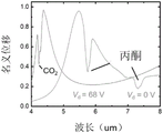
本申请实施例中,为了演示FPF的气体传感,将FPF固定在一个气室上,该气室位于FTIR的光路上,当FPF光谱在0和68V处调谐时,1.48μm的共振峰位移分别覆盖了4.26和5.75μm处的CO2和丙酮的主要分子指纹,如图7d所示,这两种气体可以在人体呼出气中进行监测,用于医疗保健等应用。带有供气和电气连接的整个测试装置如图8所示。In the embodiment of this application, in order to demonstrate the gas sensing of the FPF, the FPF is fixed on a gas chamber, which is located on the optical path of the FTIR. When the FPF spectrum is tuned at 0 and 68V, the resonance peak shift of 1.48 μm is respectively The main molecular fingerprints of CO2 and acetone at 4.26 and 5.75 μm are covered, as shown in Fig. 7d, and these two gases can be monitored in human exhaled breath for applications such as healthcare. The entire test setup with gas supply and electrical connections is shown in Figure 8.
可以知晓,本申请上述滤光片制作方法,通过将转移印刷结合到光谱滤光片中,将图案化顶部光子晶体板和底部光子晶体板放置于间隔物和基板上,通过转移印刷将图案化的硅膜从光子晶体板上转移到间隔物和基板上,从而避免微加工方法导致重复薄膜沉积引起的应力问题,同时通过转移印刷得到的滤光片可以通过改变驱动电压值对光谱的腔长位移进行调控,从而可以调控滤光片的光学性能参数。It can be known that the above-mentioned optical filter manufacturing method of the present application combines the transfer printing into the spectral filter, places the patterned top photonic crystal plate and the bottom photonic crystal plate on the spacer and the substrate, and transfers the patterned photonic crystal plate by transfer printing. The silicon film is transferred from the photonic crystal plate to the spacer and the substrate, thereby avoiding the stress problem caused by repeated thin film deposition caused by the microfabrication method, and the optical filter obtained by transfer printing can change the cavity length of the spectrum by changing the driving voltage value The displacement is adjusted, so that the optical performance parameters of the filter can be adjusted.
本申请实施例进一步提供一种光谱重建方法,包括:The embodiment of the present application further provides a spectral reconstruction method, including:
S31:向上所示的滤光片施加不同电压,并采集被测样品的光谱信息;S31: apply different voltages to the filter shown above, and collect the spectral information of the measured sample;
S32:根据所述光谱信息重建标准透射光谱。S32: Reconstruct a standard transmission spectrum according to the spectral information.
优选实施例中,由于CO2在较宽的MIR范围内包含单一且强的吸收峰,同时,气体的RI几乎为1,因此它不会引入额外的反射,从而使重建成为可能因,此 CO2是理想的目标分析物,本申请重构的光谱信息为CO2的透射光谱。In the preferred embodiment, since CO contains a single and strong absorption peak in a wide MIR range, at the same time, the RI of the gas is almost 1, so it does not introduce additional reflections, thus making the reconstruction possible. Therefore, this CO 2 is an ideal target analyte, and the spectral information reconstructed in this application is the transmission spectrum of CO 2 .
具体的,可以利用重构矩阵,重构矩阵中每个数据为一个FPF光谱的调谐状态数据,例如对于5x5的重构矩阵而言,其中包含25个FPF光谱的调谐状态。Specifically, a reconstruction matrix may be used, and each data in the reconstruction matrix is the tuning state data of one FPF spectrum, for example, for a 5x5 reconstruction matrix, there are 25 tuning states of the FPF spectrum.
由于当FPF共振峰远离特征CO2峰时,CO2吸收引起的强度变化较小,测量的强度矢量对噪声更敏感,因此本申请实施例选择了FPF共振峰接近CO2峰的部分调谐状态,而不是图7(b)中的完整调谐光谱。Since when the FPF resonance peak is far away from the characteristic CO peak, the intensity change caused by CO absorption is small, and the measured intensity vector is more sensitive to noise, so the embodiment of the present application selects a partial tuning state in which the FPF resonance peak is close to the CO peak, instead of the full tuned spectrum in Fig. 7(b).
可以看出,正是由于本申请的可调谐法布里佩罗滤光片,因此可以通过施加不同电压以达到不同调谐状态,从而在一个滤光片上即可获得丰富的光谱信息,无需大量像素提供光谱数据。It can be seen that precisely because of the tunable Fabry Perot filter of the present application, different tuning states can be achieved by applying different voltages, thereby obtaining rich spectral information on one filter without requiring a large number of Pixels provide spectral data.
图9b是F的相关系数,计算公式为
本申请将4到5μm的传输总结为强度矢量,以模拟使用波长不敏感的探测器 (如热电堆或测辐射热计)的集成系统,使用具有广义交叉验证的迭代Tikhonov 正则化方法进行重建。应用边界条件将恢复的光谱限制在0和1之间,这可以在此处用于重建传输模式下的CO2指纹。This application summarizes the 4 to 5 μm transport as an intensity vector to simulate integrated systems using wavelength-insensitive detectors such as thermopiles or bolometers, reconstructed using an iterative Tikhonov regularization method with generalized cross-validation. Boundary conditions were applied to constrain the recovered spectra between 0 and 1, which can be used here to reconstruct the CO2 fingerprint in transport mode.
图9d显示了带有测量参考光谱的恢复光谱,170nmFWHM的下降与4.26μm 处的CO2指纹相匹配,为了确定对光谱分辨率造成限制的因素,进行了两项调查。首先,研究了测量噪声如何使重建失真,在图10a中,CO2光谱是用图9a中的滤波器矩阵重建的,但不同百分比的随机噪声被添加到强度向量中。随着噪声水平从2.5%降低到0%,恢复的光谱逐渐收敛到测量的CO2光谱,均方误差(MSE)从 0.017降低到1.1x10⁻⁴。MSE定义为
图10b通过将测量强度与理想强度进行比较,揭示了25个测量调谐状态下的噪声水平,理想强度是过滤器矩阵和参考CO2光谱的乘积相加。Figure 10b reveals the noise level at the 25 measured tuning states by comparing the measured intensity with the ideal intensity, which is the sum of the products of the filter matrix and the reference CO2 spectrum.
本申请为了进一步确定此重建中的整体噪声水平,通过将重建的频谱与从不同噪声水平恢复的频谱进行比较,将平均噪声提取为0.4%。这0.4%的噪声主要归因于FTIR的测量噪声,另一个潜在原因是每次施加电压时位移变化很小,导致共振峰位置不一致。To further determine the overall noise level in this reconstruction, the applicant extracted the average noise as 0.4% by comparing the reconstructed spectrum with the spectrum recovered from different noise levels. This 0.4% noise is mainly attributable to the measurement noise of the FTIR, another potential cause is that the displacement changes very little each time a voltage is applied, resulting in inconsistent formant positions.
其次,在没有任何噪声的理想情况下研究了所需的最小调谐状态数,在图10 (c)中,在没有噪声但具有不同数量的输入状态的情况下重建具有30nm的 FWHM的高斯倾角,这些输入状态来自模拟光谱。Second, the required minimum number of tuning states is studied in the ideal case without any noise, in Fig. 10(c), the Gaussian dip with FWHM of 30 nm is reconstructed without noise but with a different number of input states, These input states come from simulated spectra.
本申请中,具有10和25个状态的重建的MSE为9.8x10⁻³和7x10⁻⁵,可以看出,当输入状态从10增加到25时,MSE提高了两个数量级。图10d显示了阶跃函数极端情况的重建结果,类似地,25个状态可以在分辨率上提供良好的重建改进,最小状态数也可以通过采样理论来预测,因此,当前的重建分辨率不受调谐级数的限制,而是受测量噪声的限制。为了进一步提高重建精度,可以采用更高的FPF共振模式,具有更多的共振峰。同时存在多个不同阶的共振峰也可以在调谐范围保持不变的情况下采样更宽的光谱,重建算法也可以优化以获得更好的噪声容限。In this application, the MSEs of the reconstructions with 10 and 25 states are 9.8x10 -3 and 7x10 -5 , and it can be seen that when the input states increase from 10 to 25, the MSE improves by two orders of magnitude. Figure 10d shows the reconstruction results for the extreme case of the step function. Similarly, 25 states can provide a good reconstruction improvement in resolution, and the minimum number of states can also be predicted by sampling theory. Therefore, the current reconstruction resolution is not affected by is limited by the number of tuning stages, but by the measurement noise. To further improve the reconstruction accuracy, higher FPF resonance modes can be employed, with more formants. The simultaneous presence of multiple formants of different orders can also sample a wider spectrum while keeping the tuning range constant, and the reconstruction algorithm can also be optimized for better noise tolerance.
本申请中计算重建的机制如图1(c)所示。首先测量各种电压下FFF的光谱为m×n校准矩阵F,其中每行是相应电压下的FPF频谱。这些光谱被归一化为背景,以便光源的光谱和探测器的响应被抵消。The mechanism of computational reconstruction in this application is shown in Figure 1(c). Firstly, the spectrum of FFF under various voltages is measured as an m×n calibration matrix F, where each row is the FPF spectrum under the corresponding voltage. These spectra are normalized to the background so that the spectra of the light source and the response of the detector cancel out.
当入射辐射时T(λ)含有未知信息的分子指纹照射FPF,其透射强度可谓I=∫F(λ)T(λ)dλ≈∑iF(λi)T(λi).后者是测量中的离散格式,并且F(λ)i是FPF频谱。当施加电压来调谐间隙并从而改变FFF的谐振峰时,每个电压处的发射强度可以通过以下方式描述:

光谱重建如图1所示,测量数据可以用下面的矩阵形式表示:The spectral reconstruction is shown in Figure 1, and the measurement data can be expressed in the following matrix form:
FT=IFT=I
其中Fisam×n矩阵,I=[I1,I2,…,Im]T是测量强度的已知矢量,T是要重建的未知光谱的矢量,由下式给出:where Fisam x n matrix, I = [I 1 , I 2 , .
T=[T1,T2,…,Tn]T T=[T 1 , T 2 ,..., T n ] T
目标是找出向量中每个元素的值,由于超定(m>>n)并且可能是错误状态的,因此此处采用Tikhonov正则化(也称为岭回归)来选择性地抑制噪声分量,该问题等价于解决具有调节因子的惩罚最小二乘问题γ:The goal is to find the value of each element in the vector. Since it is overdetermined (m>>n) and may be wrong, Tikhonov regularization (also known as ridge regression) is used here to selectively suppress the noise component. The problem is equivalent to solving the penalized least squares problem γ with a conditioning factor:

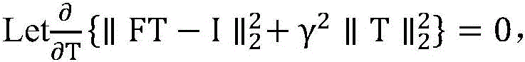

为了自适应地选择调节因子,使用了广义交叉验证(GCV)方法,在 Tikhonov正则化中,来自交叉验证的最优正则化因子可以表示为:In order to adaptively select the adjustment factor, the generalized cross-validation (GCV) method is used. In Tikhonov regularization, the optimal regularization factor from cross-validation can be expressed as:

A(γ)=F(FTF+γ2I0)-1FT A(γ)=F(F T F+γ 2 I 0 ) -1 F T
考虑到本应用中的物理情况,向量的每个元素通过施加边界条件被限制在0 和1之间。GCV用于内部迭代,每次外部迭代都会产生一个符合边界条件的新近似解。Considering the physics in this application, each element of the vector is constrained between 0 and 1 by imposing boundary conditions. GCV is used for inner iterations, and each outer iteration produces a new approximate solution that meets the boundary conditions.
进一步的,在本申请中,转移印刷FPF具有在中红外范围的波长可扩展性。利用电磁波的可扩展性和转移印刷方法,所提出的可调谐法布里佩罗滤光片可以覆盖从2到20μm的整个中红外范围,通过改变PCS反射器的设计(周期、半径、厚度以及排列方式等几何参数),可以形成各种FPF,如图12所示。它们的关键设计参数总结在下表1中:Further, in this application, the transfer printed FPF has wavelength scalability in the mid-infrared range. Using the scalability of electromagnetic waves and the transfer printing method, the proposed tunable Fabry Perot filter can cover the entire mid-infrared range from 2 to 20 μm by changing the design of the PCS reflector (period, radius, thickness, and Arrangement and other geometric parameters), various FPFs can be formed, as shown in Figure 12. Their key design parameters are summarized in Table 1 below:
表1-2到20μm之间的FPF参数Table 1-2 FPF parameters between 20μm


可以理解,目前制造所需的空气间距以匹配共振波长相当具有挑战性,尤其是当工作波长移动到大于8μm时,超过4μm的间距很难通过牺牲层的沉积来实现。本申请所提出的转移印刷技术可以解决这个限制,本申请FPF腔体间距是由硅间隔物决定的,硅间隔物是选定的SOI晶片的器件层,同时,SOI的器件层可达到的厚度没有限制。进一步的,虽然FPF大多都是静电驱动的,但拉入效应将调谐范围限制为空气间距的1/3。Understandably, it is currently quite challenging to fabricate the required air spacing to match the resonant wavelength, especially as the operating wavelength shifts beyond 8 μm, and spacings beyond 4 μm are difficult to achieve with the deposition of sacrificial layers. The transfer printing technology proposed in this application can solve this limitation. The FPF cavity spacing of this application is determined by the silicon spacer, which is the device layer of the selected SOI wafer. At the same time, the thickness of the device layer of SOI can reach no limit. Further, although most FPFs are electrostatically driven, the pull-in effect limits the tuning range to 1/3 of the air gap.
此外,可以理解的是,其他的微机电系统(MEMS)驱动方案,如压电驱动器、电磁驱动器等,也可以在可调FPF中采用,以调整间隙,从而调整共振峰。In addition, it is understood that other MEMS drive schemes, such as piezoelectric actuators, electromagnetic actuators, etc., can also be employed in the tunable FPF to adjust the gap and thus the formant.
从上述实施例可以看出,本申请实施例为了避免表面微加工方法中重复薄膜沉积引起的应力问题,采用单层PCS代替DBR作为反射器,同时通过转移印刷而不是释放牺牲层形成气腔,通过施加70V,峰值波长从5.61调整到4.13μm,覆盖了CO2和丙酮的分子指纹,验证发现可以实现CO2光谱从4到5μm的光谱重构,在4.26μm处恢复了170nm的FWHM下降。It can be seen from the above examples that in order to avoid the stress problem caused by repeated film deposition in the surface micromachining method, the embodiment of the present application uses a single-layer PCS instead of DBR as a reflector, and at the same time forms an air cavity by transfer printing instead of releasing a sacrificial layer, By applying 70 V, the peak wavelength was tuned from 5.61 to 4.13 μm, covering the molecular fingerprints of CO2 and acetone. It was verified that spectral reconstruction of the CO2 spectrum from 4 to 5 μm could be achieved, and the FWHM drop of 170 nm was recovered at 4.26 μm.
此外,值得注意的是,单层PCS仅仅作为一种典型的纳米光子反射器来构成 FPF。其他的单层薄膜反射板和单层纳米光子反射器如亚波长光栅 (SubwavelengthGrating,SWG),等离子体谐振器(Plasmonicresonator)也可以用作设计FPF的顶层板和底层板,从而实现腔体内红外光的谐振。In addition, it is worth noting that the single-layer PCS is only used as a typical nanophotonic reflector to constitute the FPF. Other single-layer thin-film reflectors and single-layer nanophoton reflectors such as subwavelength gratings (SubwavelengthGrating, SWG), plasmonic resonators (Plasmonicresonators) can also be used as the top and bottom plates of the FPF design, so as to realize the infrared light in the cavity resonance.
进一步的,本申请还提供一种微型计算中红外光谱仪,其包括单个可调谐法布里佩罗滤光片,其具体用于VOC检测、痕量气体检测、医学诊断、环境监测以及工业过程控制等。Further, the present application also provides a micro-computing mid-infrared spectrometer, which includes a single tunable Fabry Perot filter, which is specifically used for VOC detection, trace gas detection, medical diagnosis, environmental monitoring and industrial process control Wait.
需要说明的是,本发明实施例提供的显示装置实施例、测试方法实施例和测试电路实施例均可以相互参考,本申请实施例对此不做限定。本申请实施例提供的显示面板的测试方法实施例的步骤能够根据情况进行相应增减,任何熟悉本技术领域的技术人员在本申请揭露的技术范围内,可轻易想到变化的方法,都应涵盖在本申请的保护范围之内,因此不再赘述。It should be noted that the embodiment of the display device, the embodiment of the test method, and the embodiment of the test circuit provided in the embodiment of the present invention can all refer to each other, and this embodiment of the present application does not limit it. The steps of the embodiment of the test method of the display panel provided in the embodiment of the application can be increased or decreased accordingly according to the situation. Any person familiar with the technical field can easily think of a change method within the technical scope disclosed in the application, which should cover Within the protection scope of the present application, so no more details are given.
以上所述仅为本申请的可选实施例,并不用以限制本申请,凡在本申请的精神和原则之内,所作的任何修改、等同替换、改进等,均应包含在本申请的保护范围之内。The above are only optional embodiments of the application, and are not intended to limit the application. Any modifications, equivalent replacements, improvements, etc. made within the spirit and principles of the application shall be included in the protection of the application. within range.
Claims (11)
Applications Claiming Priority (2)
| Application Number | Priority Date | Filing Date | Title |
|---|---|---|---|
| SG10202105952R | 2021-06-04 | ||
| SG10202105952R | 2021-06-04 |
Publications (1)
| Publication Number | Publication Date |
|---|---|
| CN115507948A true CN115507948A (en) | 2022-12-23 |
Family
ID=84441767
Family Applications (1)
| Application Number | Title | Priority Date | Filing Date |
|---|---|---|---|
| CN202210621430.XA Pending CN115507948A (en) | 2021-06-04 | 2022-06-02 | Optical filter of spectrometer, manufacturing method and spectrum reconstruction method |
Country Status (2)
| Country | Link |
|---|---|
| JP (1) | JP2022186672A (en) |
| CN (1) | CN115507948A (en) |
Citations (9)
| Publication number | Priority date | Publication date | Assignee | Title |
|---|---|---|---|---|
| US6373632B1 (en) * | 2000-03-03 | 2002-04-16 | Axsun Technologies, Inc. | Tunable Fabry-Perot filter |
| US20050226281A1 (en) * | 2002-03-08 | 2005-10-13 | Lorenzo Faraone | Tunable cavity resonator and method of fabricating same |
| KR20070047596A (en) * | 2005-11-02 | 2007-05-07 | 한국기계연구원 | Silicon Fabry-Perot Wavelength Tunable Filter Using Thermo-optic Phenomena and Manufacturing Method Thereof |
| US20120268809A1 (en) * | 2011-04-20 | 2012-10-25 | Lingjie Jay Guo | Spectrum filtering for visual displays and imaging having minimal angle dependence |
| US20130240708A1 (en) * | 2012-03-14 | 2013-09-19 | Kabushiki Kaisha Toshiba | Solid-state image pickup device and method of manufacturing solid-state image pickup device |
| US20140111811A1 (en) * | 2011-06-06 | 2014-04-24 | Mikko Tuohiniemi | Micromechanical tunable fabry-perot interferometer and a method for producing the same |
| CN106772751A (en) * | 2017-01-03 | 2017-05-31 | 杭州科汀光学技术有限公司 | A kind of quasi- Rugate filter of wavelength spacing gradual change |
| US20170276996A1 (en) * | 2014-08-25 | 2017-09-28 | Montana State University | Microcavity array for spectral imaging |
| CN111174909A (en) * | 2020-01-19 | 2020-05-19 | 深圳奥比中光科技有限公司 | Optical filter, imaging device and electronic equipment |
-
2022
- 2022-06-02 CN CN202210621430.XA patent/CN115507948A/en active Pending
- 2022-06-03 JP JP2022090880A patent/JP2022186672A/en not_active Withdrawn
Patent Citations (9)
| Publication number | Priority date | Publication date | Assignee | Title |
|---|---|---|---|---|
| US6373632B1 (en) * | 2000-03-03 | 2002-04-16 | Axsun Technologies, Inc. | Tunable Fabry-Perot filter |
| US20050226281A1 (en) * | 2002-03-08 | 2005-10-13 | Lorenzo Faraone | Tunable cavity resonator and method of fabricating same |
| KR20070047596A (en) * | 2005-11-02 | 2007-05-07 | 한국기계연구원 | Silicon Fabry-Perot Wavelength Tunable Filter Using Thermo-optic Phenomena and Manufacturing Method Thereof |
| US20120268809A1 (en) * | 2011-04-20 | 2012-10-25 | Lingjie Jay Guo | Spectrum filtering for visual displays and imaging having minimal angle dependence |
| US20140111811A1 (en) * | 2011-06-06 | 2014-04-24 | Mikko Tuohiniemi | Micromechanical tunable fabry-perot interferometer and a method for producing the same |
| US20130240708A1 (en) * | 2012-03-14 | 2013-09-19 | Kabushiki Kaisha Toshiba | Solid-state image pickup device and method of manufacturing solid-state image pickup device |
| US20170276996A1 (en) * | 2014-08-25 | 2017-09-28 | Montana State University | Microcavity array for spectral imaging |
| CN106772751A (en) * | 2017-01-03 | 2017-05-31 | 杭州科汀光学技术有限公司 | A kind of quasi- Rugate filter of wavelength spacing gradual change |
| CN111174909A (en) * | 2020-01-19 | 2020-05-19 | 深圳奥比中光科技有限公司 | Optical filter, imaging device and electronic equipment |
Non-Patent Citations (1)
| Title |
|---|
| 温志渝;陈刚;王建国;: "基于Fabry-Perot腔阵列的集成化微型光谱仪方案及模拟", 光谱学与光谱分析, no. 10, 28 October 2006 (2006-10-28) * |
Also Published As
| Publication number | Publication date |
|---|---|
| JP2022186672A (en) | 2022-12-15 |
Similar Documents
| Publication | Publication Date | Title |
|---|---|---|
| US11543653B2 (en) | Device components formed of geometric structures | |
| US7826120B2 (en) | Method and device for multi-color interferometric modulation | |
| US7830587B2 (en) | Method and device for modulating light with semiconductor substrate | |
| US7379227B2 (en) | Method and device for modulating light | |
| KR100853131B1 (en) | Method and apparatus for driving an electronic device | |
| CN103293660B (en) | Miniature F-P (Fabry-Perot) cavity tunable filter and method for manufacturing same | |
| US20060261330A1 (en) | MEMS device and method of forming a MEMS device | |
| US20080088912A1 (en) | System and method for a mems device | |
| US20060268388A1 (en) | Movable micro-electromechanical device | |
| US20080088911A1 (en) | System and method for a mems device | |
| US20080088910A1 (en) | System and method for a mems device | |
| US20120062310A1 (en) | System and method for charge control in a mems device | |
| JP7268880B2 (en) | Spectroscopic device integrated with transmission waveguide mode resonance grating and manufacturing method thereof | |
| US20220171105A1 (en) | Resonant filters having simultaneously tuned central wavelengths and sidebands | |
| US20100245980A1 (en) | System and method for a mems device | |
| US7800809B2 (en) | System and method for a MEMS device | |
| Tripathi et al. | Large-area MEMS-based distributed Bragg reflectors for short-wave and mid-wave infrared hyperspectral imaging applications | |
| CN112415647B (en) | Semiconductor etalon device and manufacturing method | |
| CN115507948A (en) | Optical filter of spectrometer, manufacturing method and spectrum reconstruction method | |
| Silva et al. | Silicon-air-silicon DBRs for electrostatically actuated infrared filter applications | |
| CN117213633B (en) | A full-band computational reconstruction spectrometer based on MEMS in-plane driving | |
| CN114014255B (en) | Micro-nano structure with spectral response | |
| Chang et al. | Transfer-printed NEMS tunable Fabry Pérot filter for mid-infrared computational spectroscopy | |
| Nagao et al. | Wavelength-selective photothermal infrared sensors | |
| Milne et al. | MEMS-based tunable Fabry-Perot filters on silicon substrates |
Legal Events
| Date | Code | Title | Description |
|---|---|---|---|
| PB01 | Publication | ||
| PB01 | Publication | ||
| SE01 | Entry into force of request for substantive examination | ||
| SE01 | Entry into force of request for substantive examination | ||
| WD01 | Invention patent application deemed withdrawn after publication | ||
| WD01 | Invention patent application deemed withdrawn after publication |
Application publication date: 20221223 |