Disclosure of Invention
The application provides an image sensor and a preparation method thereof, which can solve the problem of charge escape of a CMOS image sensor.
In one aspect, an embodiment of the present application provides a method for manufacturing an image sensor, including:
providing a substrate, wherein a photodiode region is formed in the substrate, a sacrificial oxide layer and a grid electrode are formed on the substrate, the sacrificial oxide layer covers the surface of the substrate, the grid electrode is positioned on the sacrificial oxide layer, and the projection of the grid electrode on the surface of the substrate covers the photodiode region;
forming a first clamping region on the photodiode region in the substrate;
forming a first side wall layer and a second side wall layer, wherein the first side wall layer covers the grid and the surface of the substrate, and the second side wall layer is positioned on the first side wall layer on the side surface of the grid;
forming a first patterned photoresist layer, wherein the first patterned photoresist layer opens a first window on the second side wall layer on the photodiode region;
according to the first window, performing an ion implantation process on the substrate to form a second clamping area on the first clamping area;
continuing to perform an ion implantation process on the substrate according to the first window to form a barrier layer on the second clamping area;
removing the first patterned photoresist layer;
and carrying out a wet cleaning process on the surface of the first side wall layer and the surface of the second side wall layer.
Optionally, in the manufacturing method of the image sensor, a Co-C ion implantation process is continuously performed on the substrate according to the first window to form a barrier layer on the second clamping region.
Optionally, in the manufacturing method of the image sensor, in the process of performing a Co-C ion implantation process on the substrate to form a barrier layer on the second clamping region, implantation energy of the Co-C ion implantation process is 4kev to 8kev; the dosage of the implanted carbon ions is 0.5E15atoms/cm2~1E15 atoms/cm2。
Optionally, in the preparation method of the image sensor, O is used2And H2N2The first patterned photoresist layer is removed by ashing with the mixed gas.
Optionally, in the method for manufacturing the image sensor, a wet cleaning process is performed on the surface of the first sidewall layer and the surface of the second sidewall layer by using SPM and SC1 to remove the residual metal ions and the first patterned photoresist layer.
Optionally, in the method for manufacturing an image sensor, the first patterned photoresist layer has a thickness of
Optionally, in the method for manufacturing an image sensor, after the wet cleaning process is performed on the surface of the first sidewall layer and the surface of the second sidewall layer, the method for manufacturing an image sensor further includes:
and carrying out a thermal annealing process on the image sensor after the barrier layer is formed.
Optionally, in the method for manufacturing an image sensor, the step of forming a first clamping region on the photodiode region in the substrate includes:
forming a second patterned photoresist layer that opens a second window on the gate side over the photodiode region;
according to the second window, performing an ion implantation process on the substrate to form a first clamping area on the photodiode area;
and removing the second patterned photoresist layer.
Optionally, in the method for manufacturing an image sensor, after performing a wet cleaning process on the surface of the first sidewall layer and the surface of the second sidewall layer, the method for manufacturing an image sensor further includes:
and carrying out wafer brushing technology on the surface of the first side wall layer and the surface of the second side wall layer to remove residual polymer particles.
On the other hand, an embodiment of the present application further provides an image sensor, including:
the photoelectric diode device comprises a substrate, wherein a photoelectric diode region is formed in the substrate, a sacrificial oxide layer and a grid electrode are further formed on the substrate, the sacrificial oxide layer covers the surface of the substrate, the grid electrode is located on the sacrificial oxide layer, and the projection of the grid electrode on the surface of the substrate covers the photoelectric diode region;
a first clamping region on the photodiode region in the substrate;
the first side wall layer covers the grid and the surface of the substrate, and the second side wall layer is positioned on the first side wall layer on the side surface of the grid;
a second clamping region located on the first clamping region in the substrate;
a barrier layer located on the second clamping region in the substrate.
The technical scheme at least comprises the following advantages:
the invention provides a preparation method of an image sensor, which comprises the following steps: providing a substrate, wherein a photodiode region is formed in the substrate, and a sacrificial oxide layer and a grid electrode are also formed on the substrate; forming a first clamping area; forming a first side wall layer and a second side wall layer; forming a first patterned photoresist layer to open a first window on the photodiode region; performing an ion implantation process to form a second clamping region on the first clamping region; continuing to perform an ion implantation process to form a barrier layer on the second clamping area; removing the first patterned photoresist layer; and carrying out a wet cleaning process on the surface of the first side wall layer and the surface of the second side wall layer. By performing the ion implantation process on the substrate to form the second clamping area on the first clamping area and continuing to perform the ion implantation process to form the barrier layer on the second clamping area, the second clamping area can play a good role in isolation, and fluorine ions in the second clamping area can trap defects and inhibit diffusion of conductive ions doped in the substrate. Furthermore, the blocking layer can inhibit ion diffusion in the second clamping area on one hand, and can trap interstitial silicon atoms and other defect positions on the other hand, so that diffusion and escape of boron/fluorine ions caused by a subsequent thermal annealing process can be inhibited, escape of photoelectrons is inhibited, white noise points are improved, and the problem of charge escape of the CMOS image sensor is solved.
Detailed Description
The technical solutions in the present application will be described clearly and completely with reference to the accompanying drawings, and it is obvious that the described embodiments are some, but not all embodiments of the present application. All other embodiments obtained by a person of ordinary skill in the art based on the embodiments in the present application without making creative efforts belong to the protection scope of the present application.
In the description of the present application, it should be noted that the terms "center", "upper", "lower", "left", "right", "vertical", "horizontal", "inner", "outer", and the like indicate orientations or positional relationships based on the orientations or positional relationships shown in the drawings, and are only for convenience of description and simplicity of description, and do not indicate or imply that the device or element being referred to must have a particular orientation, be constructed and operated in a particular orientation, and thus, should not be construed as limiting the present application. Furthermore, the terms "first," "second," and "third" are used for descriptive purposes only and are not to be construed as indicating or implying relative importance.
In the description of the present application, it should be noted that, unless otherwise explicitly stated or limited, the terms "mounted," "connected," and "connected" are to be construed broadly, and may be, for example, a fixed connection, a detachable connection, or an integral connection; the connection can be mechanical connection or electrical connection; the two elements may be directly connected or indirectly connected through an intermediate medium, or may be communicated with each other inside the two elements, or may be wirelessly connected or wired connected. The specific meaning of the above terms in the present application can be understood in a specific case by those of ordinary skill in the art.
In addition, the technical features mentioned in the different embodiments of the present application described below may be combined with each other as long as they do not conflict with each other.
An embodiment of the present application provides a method for manufacturing an image sensor, and referring to fig. 1, fig. 1 is a flowchart of a method for manufacturing an image sensor according to an embodiment of the present invention, where the method for manufacturing an image sensor includes:
step S10: providing a substrate, wherein a photodiode region is formed in the substrate, a sacrificial oxide layer and a grid electrode are formed on the substrate, the sacrificial oxide layer covers the surface of the substrate, the grid electrode is positioned on the sacrificial oxide layer, and the projection of the grid electrode on the surface of the substrate covers the photodiode region;
step S20: forming a first clamping region on the photodiode region in the substrate;
step S30: forming a first side wall layer and a second side wall layer, wherein the first side wall layer covers the grid and the surface of the substrate, and the second side wall layer is positioned on the first side wall layer on the side surface of the grid;
step S40: forming a first patterned photoresist layer, wherein the first patterned photoresist layer opens a first window on the second sidewall layer on the photodiode region;
step S50: according to the first window, performing an ion implantation process on the substrate to form a second clamping area on the first clamping area;
step S60: continuing to perform an ion implantation process on the substrate according to the first window to form a barrier layer on the second clamping area;
step S70: removing the first patterned photoresist layer;
step S80: and carrying out a wet cleaning process on the surface of the first side wall layer and the surface of the second side wall layer.
Specifically, referring to fig. 2-11, fig. 2-11 are schematic semiconductor diagrams in various process steps for manufacturing an image sensor according to an embodiment of the present invention.
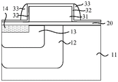
First, referring to fig. 2, a substrate 11 is provided, a deep well region 12 is formed in the substrate 11, a photodiode region 13 is formed on the deep well region, a sacrificial oxide layer 20 and a gate 31 are formed on the substrate 11, wherein the sacrificial oxide layer 20 covers the surface of the substrate 11, the gate 31 is located on the sacrificial oxide layer 20, and the gate 31 covers the photodiode region 13 on the top-down projection of the surface of the substrate 11. In this embodiment, the material of the substrate 11 may be monocrystalline silicon, the substrate 11 may include a base and an epitaxial layer located on the base, and both the deep well region 12 and the photodiode region 13 may be formed in the epitaxial layer. The deep well region 12 may be an N-type deep well region, and the photodiode region 13 may be an N + type photodiode region. The doped ions in the N-type deep well region 12 and the N + type photodiode region 13 may be N-type conductive ions such as arsenic ions and phosphorous ions. The gate electrode 31 on the photodiode region 13 of the present embodiment may be a transfer gate (TX).
Then, referring to fig. 3, a second patterned photoresist layer 40 is formed, and the second patterned photoresist layer 40 opens a second window on the gate electrode 31 side on the photodiode region 13.
Next, referring to fig. 4, according to the second window, an ion implantation process is performed on the substrate 11 to form a first clamping region 14 on the photodiode region 13. P-type conductive ions (e.g., boron ions) are implanted into the substrate 11 to form a first clamping region 14 on the photodiode region 13.
Further, referring to fig. 5, the second patterned photoresist layer 40 is removed.
Next, referring to fig. 6, a first sidewall layer 32 and a second sidewall layer 33 are formed, the first sidewall layer 32 covers the gate electrode 31 and the surface of the substrate 11, and the second sidewall layer 33 is located on the first sidewall layer 32 at the side of the gate electrode 31. The material of the first sidewall layer 32 may be silicon oxide, and the material of the second sidewall layer 33 may be silicon nitride.
Further, referring to fig. 7, a first
patterned photoresist layer 50 is formed, and the first
patterned photoresist layer 50 opens a first window on the
second sidewall layer 33 on the photodiode region 13 (the first clamping region 14). Preferably, the first
patterned photoresist layer 50 may have a thickness of
For example
Next, referring to fig. 8, an ion implantation process is performed on the substrate 11 according to the first window to form a second clamping region 15 on the first clamping region 14. In the present embodiment, the substrate 11 is implanted with P-type conductive ions (e.g., boron ions, BF may be used as the ion source)2) To form a second clamping area 15 on said first clamping area 14. Wherein the second clamping area 15 can play a good isolation role, and fluorine ions can trap defects, inhibiting diffusion of conductive ions doped in the substrate 11.
Further, referring to fig. 9, continuing with the first window, an ion implantation process is performed on the substrate 11 to form a barrier layer 16 on the second clamping area 15.
Preferably, the present embodiment continues with performing a Co-C ion implantation process on the substrate according to the first window to form a barrier layer 16 on the second clamping region 15. Specifically, in the process of performing a Co-C ion implantation process on the substrate to form the barrier layer 16 on the second clamping region 15, the implantation energy of the Co-C ion implantation process may be 4kev to 8kev; the dosage of the implanted carbon ions can be 0.5E15atoms/cm2~1E15 atoms/cm2。
Next, referring to fig. 10, the first patterned photoresist layer 50 is removed. Specifically, this embodiment may utilize O2And H2N2The first patterned photoresist layer 50 is removed by ashing with the mixed gas.
Finally, a wet cleaning process is performed on the surface of the first sidewall layer 32 and the surface of the second sidewall layer 33 (formed semiconductor structure). In this embodiment, a wet cleaning process is performed on the surface of the first sidewall layer and the surface of the second sidewall layer by using SPM and SC1 to remove the residual metal ions and the first patterned photoresist layer 50.
Further, referring to fig. 11, after performing a wet cleaning process on the surface of the first sidewall layer 32 and the surface of the second sidewall layer 33, the method for manufacturing an image sensor according to the embodiment of the present application may further include: source-drain regions 17 are formed, and in the present embodiment, the source-drain regions 17 are floating diffusion regions (FDs). The conductivity type of the source drain region 17 may be N type.
In this embodiment, the conventional process steps of forming the reset gate, the source follower gate, the gate tube gate, and the respective bottom active regions of the image sensor, and the conventional preparation processes of AA, photo, IMP, POLY, CT, and Metal required for preparing CIS may also be included.
Preferably, after performing a wet cleaning process on the surface of the first sidewall layer 32 and the surface of the second sidewall layer 33 or forming the source drain region 17, the method for manufacturing an image sensor according to the embodiment of the present application may further include: and carrying out a thermal annealing process on the semiconductor structure after the barrier layer 16 is formed. As can be seen from fig. 10, during the thermal annealing process, the lattice repair of the surface layer (silicon surface layer) of the substrate 11 promotes the diffusion of boron/fluorine ions to the silicon surface, and after Co — C ion (carbon Co-ion) implantation, the barrier layer 16 rich in carbon ions can inhibit the diffusion of boron/fluorine ions; further, the carbon ions can trap interstitial silicon atoms and other defect sites, so that the diffusion and the escape of boron ions/fluorine ions caused by annealing are inhibited, the escape of photoelectrons is inhibited, and white pixel is improved. The inventor researches and discovers that the concentration of boron ions near the 7nm depth of the substrate is from 1.3x10 along with the increase of the dosage of the carbon ions20atoms/cm3Increase to 1.9x10²⁰ atoms/cm3This demonstrates that the cco-Implant can effectively inhibit boron ion diffusion in the second clamping region. Further, the inventors have also found that Co-C ions (C) are carried outCarbon co-Ion) implantation process, the leakage current is effectively reduced when the Ion of the NMOS is the same.
Preferably, after performing a wet cleaning process on the surface of the first sidewall layer 32 and the surface of the second sidewall layer 33 or forming the source drain region 17, the method for manufacturing an image sensor according to the embodiment of the present application may further include: and carrying out a wafer brushing process on the surface of the first side wall layer 32 and the surface of the second side wall layer 33 to completely remove polymer particles remained on the surface of the device.
Based on the same inventive concept, an embodiment of the present application further provides an image sensor, as shown in fig. 10, the image sensor includes:
a substrate 11, a photodiode region 13 is formed in the substrate 11, a sacrificial oxide layer 20 and a gate 31 are further formed on the substrate 11, wherein the sacrificial oxide layer 20 covers the surface of the substrate 11, the gate 31 is located on the sacrificial oxide layer 20, and the gate 31 covers the photodiode region 13 in projection on the surface of the substrate 11;
a first clamping region 14, the first clamping region 14 being located on the photodiode region 13 in the substrate 11;
a first sidewall layer 32 and a second sidewall layer 33, wherein the first sidewall layer 32 covers the gate 31 and the surface of the substrate 11, and the second sidewall layer 33 is located on the first sidewall layer 32 at the side of the gate 31;
a second clamping region 15, said second clamping region 15 being located on said first clamping region 14 in said substrate 11;
a barrier layer 16, said barrier layer 16 being located on said second clamping area 15 in said substrate 11.
In summary, the present invention provides a method for manufacturing an image sensor, including: providing a substrate 11, wherein a photodiode region 13 is formed in the substrate 11, and a sacrificial oxide layer 20 and a gate 31 are further formed on the substrate 11; forming a first clamping area 14; forming a first sidewall layer 32 and a second sidewall layer 33; forming a first patterned photoresist layer 50 to open a first window on the photodiode region 13; performing an ion implantation process to form a second clamping region 15 on the first clamping region 14; continuing to perform an ion implantation process to form a barrier layer 16 on the second clamping region 15; removing the first patterned photoresist layer 50; and performing a wet cleaning process on the surface of the first side wall layer 32 and the surface of the second side wall layer 33. The invention also provides an image sensor. By performing an ion implantation process on the substrate to form a second clamping region 15 on the first clamping region 14 and continuing to perform the ion implantation process to form a barrier layer 16 on the second clamping region 15, the second clamping region 15 can perform a good isolation function, and fluorine ions can trap defects and inhibit diffusion of conductive ions doped in the substrate 11. Further, the blocking layer 16 can suppress boron ion diffusion in the second clamping region 15 on one hand, and can trap interstitial silicon atoms and other defect sites on the other hand, so that boron/fluorine ion diffusion and escape caused by a subsequent thermal annealing process can be suppressed, further photoelectrons escape is suppressed, white noise is improved, and the problem of charge escape of the CMOS image sensor is solved.
It should be understood that the above examples are only for clarity of illustration and are not intended to limit the embodiments. Other variations and modifications will be apparent to persons skilled in the art in light of the above description. And are neither required nor exhaustive of all embodiments. And obvious variations or modifications of this invention are intended to be covered by the scope of the invention as expressed herein.