Disclosure of Invention
In order to solve the technical problem, the present disclosure provides a fully differential operational amplifier and a fully differential operational amplifier circuit, which can improve the switching frequency of the fully differential operational amplifier during the subsequent normal operation, effectively reduce the chip area, and expand the power supply voltage range of the fully differential operational amplifier, thereby enhancing the applicability of the fully differential operational amplifier in a high-speed high-precision ADC.
In one aspect the present disclosure provides a fully differential operational amplifier, comprising:
a differential input pair;
a first output module having a first output port for providing a first output voltage, the first output module being configured to adjust its own conduction state during a power-on reset of the fully differential operational amplifier, and clamp up the first output voltage to a supply voltage;
and the second output module is used for adjusting the self conduction state during the power-on reset period of the fully differential operational amplifier and clamping the second output voltage down to the ground voltage.
Preferably, the fully differential operational amplifier further comprises:
and the control switch is connected between the first output port and the second output port, is controlled by a common mode establishing signal, and is used for short-circuiting the two output ports for a short time after the establishment of the common mode reset of the fully differential operational amplifier is finished.
Preferably, the aforementioned differential input pair comprises:
a first transistor, a first end of which is connected to the power supply end through a third transistor and is connected to the power supply voltage, a second end of which is connected to the first output module, and a control end of which is connected to a first input voltage;
and a second transistor, wherein the first end of the second transistor is connected with the first end of the first transistor, the second end of the second transistor is connected with the second output module, and the control end of the second transistor is connected with a second input voltage.
Preferably, the aforementioned first output module includes:
a fourth transistor and a sixth transistor connected in series between a power supply terminal and the first output port, a control terminal of the fourth transistor being connected to a control terminal of the third transistor and commonly connected to a first bias voltage;
and the control end of the seventh transistor is connected with the control end of the sixth transistor and is commonly connected with a second bias voltage.
Preferably, the aforementioned second output module comprises:
an eighth transistor and a tenth transistor connected in series between the first output port and ground, the eighth transistor and the sixth transistor being connected with a connection node therebetween serving as the first output port for providing the first output voltage, the connection node between the eighth transistor and the tenth transistor being connected to a second terminal of the first transistor;
a ninth transistor and an eleventh transistor connected in series between the second output port and ground, wherein the ninth transistor and the seventh transistor are connected with a connection node therebetween serving as the second output port to provide the second output voltage, a control terminal of the ninth transistor and a control terminal of the eighth transistor are connected to commonly receive a third bias voltage, a control terminal of the eleventh transistor intermittently connects a control terminal of the tenth transistor through timing control and commonly receives a fourth bias voltage, and a connection node between the ninth transistor and the eleventh transistor is connected to a second terminal of the second transistor.
Preferably, the first output module further comprises:
a first switch tube connected between the control end of the fourth transistor and the control end of the fifth transistor;
and a second switching tube connected between the control end of the fifth transistor and the second end of the fifth transistor.
Preferably, the aforementioned second output module further comprises:
a third switching tube connected between a control terminal of the tenth transistor and a control terminal of the eleventh transistor;
and a fourth switching tube connected between the control terminal of the tenth transistor and the first terminal thereof.
Preferably, the first switch tube and the fourth switch tube are controlled by a first control signal,
the second switch tube and the third switch tube are controlled by a second control signal,
the first control signal and the second control signal are opposite-phase signals.
Preferably, any one of the first transistor, the second transistor, the third transistor, the fourth transistor, the fifth transistor, the sixth transistor, the seventh transistor, the eighth transistor, the ninth transistor, the tenth transistor, and the eleventh transistor is a metal oxide semiconductor field effect transistor.
Preferably, the first transistor, the second transistor, the third transistor, the fourth transistor, the fifth transistor, the eighth transistor and the ninth transistor are all P-type metal oxide semiconductor field effect transistors,
and the sixth transistor, the seventh transistor, the tenth transistor and the eleventh transistor are all N-type metal oxide semiconductor field effect transistors.
Preferably, the first switch tube and the second switch tube are both N-type field effect transistor devices,
and the third switching tube and the fourth switching tube are both P-type field effect transistor devices.
In another aspect, the present disclosure also provides a fully differential operational amplifier circuit, including:
a fully differential operational amplifier as previously described having a first output port providing a first output voltage and a second output port providing a second output voltage;
the common mode detection module is connected with the first output port and the second output port and used for obtaining an average output voltage according to the first output voltage and the second output voltage;
a comparator connected between the common mode detection module and the fully differential operational amplifier for generating a regulated voltage according to a comparison result between a preset common mode voltage and the average output voltage,
the fully differential operational amplifier controls the self-conducting state according to the regulating voltage time sequence during the power-on reset period, so that the average output voltage is stabilized at the preset common-mode voltage.
Preferably, the common mode detection module comprises:
and the switches in the switched capacitor network are matched with two-phase non-overlapping clocks to carry out multiple on-off, and stable average output voltage is obtained by utilizing the charging and discharging processes of the capacitors.
In another aspect, the present disclosure also provides a fully differential operational amplifier, including:
a differential input pair;
the input end of the first chopping switch is respectively connected with a first input voltage and a second input voltage, and the output end of the first chopping switch is respectively correspondingly connected with the control ends of the differential input pair and used for providing a high-frequency modulation signal;
the output module is provided with a first output port for providing a first output voltage and a second output port for providing a second output voltage, and demodulates and outputs the amplified high-frequency modulation signal into the first output voltage and the second output voltage by utilizing a plurality of chopping switches controlled by a plurality of paths of clock signals;
a processing module, the input end of which is connected with a plurality of control signals, the processing module is used for carrying out logic operation on the control signals to generate the multipath clock signals,
during the power-on reset period of the fully differential operational amplifier, the processing module controls the clock signal frequency of the corresponding chopping switch through the logic operation of the control signals, and pulls up the first output voltage clamp to the power supply voltage and pulls down the second output voltage clamp to the ground voltage.
Preferably, the plurality of control signals accessed by the processing module include: the first control signal rstb, the second control signal rst and the third control signal ph1,
and the generated multipath clock signal comprises: a first clock signal Ph2s, a second clock signal Ph1s, a third clock signal Ph1t, and a fourth control signal Ph2,
the first control signal rstb and the second control signal rst are inverse signals.
Preferably, the aforementioned second clock signal is: ph1s ═ ph1 × rstb,
the first clock signal is: ph2s ═ ph2 × rstb,
the third clock signal is: ph1t ═ ph1+ rst.
Preferably, the aforementioned differential input pair comprises:
a first transistor, a first end of which is connected to a power supply end through a third transistor and is connected to the power supply voltage, a second end of which is connected to the output module, and a control end of which is connected to the first chopper switch;
and a second transistor, wherein the first end of the second transistor is connected with the first end of the first transistor in a common mode, the second end of the second transistor is connected with the output module, and the control end of the second transistor is connected with the first chopping switch.
Preferably, the first chopping switch has a first input terminal, a second input terminal, a first output terminal and a second output terminal,
the first input terminal is connected to the first input voltage, the second input terminal is connected to the second input voltage, the first output terminal is connected to the control terminal of the first transistor, and the second output terminal is connected to the control terminal of the second transistor.
Preferably, the aforementioned output module includes:
a second chopper switch having a third input terminal, a fourth input terminal, a third output terminal, and a fourth output terminal, the third input terminal being connected to a power supply terminal via a fourth transistor, the fourth input terminal being connected to the power supply terminal via a fifth transistor, the third output terminal being connected to the first output port via a sixth transistor, the fourth output terminal being connected to the second output port via a seventh transistor, a control terminal of the fourth transistor and a control terminal of the fifth transistor being connected to a control terminal of the third transistor in common, the second chopper switch being connected to a first bias voltage, and a control terminal of the sixth transistor and a control terminal of the seventh transistor being connected to a second bias voltage;
and a third chopper switch having a fifth input terminal, a sixth input terminal, a fifth output terminal, and a sixth output terminal, the fifth output terminal being connected to the first output port via an eighth transistor, the sixth output terminal being connected to the second output port via a ninth transistor, the fifth input terminal being connected to ground via a tenth transistor, the sixth input terminal being connected to ground via an eleventh transistor, a control terminal of the eighth transistor being connected to a control terminal of the ninth transistor and receiving a third bias voltage, a control terminal of the tenth transistor being connected to a control terminal of the eleventh transistor and receiving a fourth bias voltage.
Preferably, the aforementioned second chopping switch comprises a first switch, a second switch, a third switch and a fourth switch,
the third input terminal is connected to the third output terminal through the first switch, and is connected to the fourth output terminal through the second switch;
the fourth input terminal is connected to the third output terminal through the third switch, and the fourth output terminal is connected to the fourth switch.
Preferably, the aforementioned third chopping switch comprises a fifth switch, a sixth switch, a seventh switch and an eighth switch,
said fifth input terminal being connected to said fifth output terminal through said fifth switch and to said sixth output terminal through said sixth switch;
the sixth input terminal is connected to the fifth output terminal via the seventh switch, and is connected to the sixth output terminal via the eighth switch.
Preferably, the first switch and the eighth switch are controlled by the third clock signal, the second switch, the third switch, the sixth switch and the seventh switch are controlled by the first clock signal, and the fourth switch and the fifth switch are controlled by the second clock signal.
Preferably, any one of the first transistor, the second transistor, the third transistor, the fourth transistor, the fifth transistor, the sixth transistor, the seventh transistor, the eighth transistor, the ninth transistor, the tenth transistor, and the eleventh transistor is a metal oxide semiconductor field effect transistor.
Preferably, the first transistor, the second transistor, the third transistor, the fourth transistor, the fifth transistor, the sixth transistor and the seventh transistor are P-type metal oxide semiconductor field effect transistors,
and the eighth transistor, the ninth transistor, the tenth transistor and the eleventh transistor are all N-type metal oxide semiconductor field effect transistors.
Preferably, the first switch, the second switch, the third switch, the fourth switch, the fifth switch, the sixth switch, the seventh switch and the eighth switch are all cmos fet devices.
In another aspect, the present disclosure also provides a fully differential operational amplifier circuit, including:
a fully differential operational amplifier as previously described.
The beneficial effect of this disclosure is: in one aspect, the present disclosure provides a fully differential operational amplifier, including: a differential input pair; the first output module is used for adjusting the self conduction state of the fully differential operational amplifier during the power-on reset period of the fully differential operational amplifier and clamping and pulling up a first output voltage to a power supply voltage; a second output module for adjusting its own conduction state during a power-on reset of the fully differential operational amplifier, clamping a second output voltage down to ground. The output module utilizes a single-tube field effect transistor device as a switch, breaks through the limitation of the size and the working voltage of the switch which uses a CMOS device in the prior art, can expand the working voltage range (low voltage limiting value) of the fully differential operational amplifier while realizing the establishment of an output common mode in the reset stage, and can also effectively reduce the integration area of the fully differential operational amplifier chip and reduce the manufacturing cost;
optionally, the added control switch connected between the first output port and the second output port is controlled by a common mode establishing signal, after the establishment of the common mode reset of the fully differential operational amplifier is finished, the two output ports are in short circuit for a short time, so that the output differential mode reset is zero through the rapid clamping control, the establishment time of the common mode voltage during the power-on reset period is shortened, the switching frequency of the fully differential operational amplifier during the subsequent normal operation is improved, and the applicability of the fully differential operational amplifier in the high-speed high-precision ADC is enhanced.
In another aspect, the present disclosure provides a chopped fully differential operational amplifier, which includes: a differential input pair; the input end of the first chopping switch is respectively connected with a first input voltage and a second input voltage, and the output end of the first chopping switch is respectively correspondingly connected with the control ends of the differential input pair and used for providing a high-frequency modulation signal; the output module demodulates and outputs the amplified high-frequency modulation signal into a first output voltage and a second output voltage by utilizing a plurality of chopping switches controlled by a plurality of paths of clock signals; and a processing module, an input end of which is connected to a plurality of control signals, the processing module being configured to perform a logic operation on the plurality of control signals to generate the plurality of clock signals, wherein during a power-on reset period of the fully differential operational amplifier, the processing module controls a clock signal frequency of a corresponding chopper switch through the logic operation on the plurality of control signals to clamp the first output voltage up to a power supply voltage and clamp the second output voltage down to a ground voltage. The existing fully differential operational amplifier with the chopping switch structure is utilized, no additional switch is added, only simple logic operation is needed to be added, the establishment of the output common-mode voltage in the reset stage can be realized, the circuit design is very simple and reliable, the purpose of shortening the establishment time of the common-mode voltage in the power-on reset period can be achieved, the switching frequency of the fully differential operational amplifier in the subsequent normal work can be improved, and the applicability of the fully differential operational amplifier in a high-speed high-precision ADC (analog to digital converter) is enhanced.
Detailed Description
To facilitate an understanding of the present disclosure, the present disclosure will now be described more fully with reference to the accompanying drawings. Preferred embodiments of the present disclosure are set forth in the accompanying drawings. However, the present disclosure may be embodied in different forms and is not limited to the embodiments described herein. Rather, these embodiments are provided so that this disclosure will be thorough and complete.
Unless defined otherwise, all technical and scientific terms used herein have the same meaning as commonly understood by one of ordinary skill in the art to which this disclosure belongs. The terminology used in the description of the disclosure herein is for the purpose of describing particular embodiments only and is not intended to be limiting of the disclosure.
The present disclosure is described in detail below with reference to the accompanying drawings.
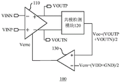
Referring to fig. 1 to 3, the fully differential operational amplifier circuit 100 includes a fully differential operational amplifier 110 and a common mode feedback loop connected to the fully differential operational amplifier 110 and operating in a two-phase clock, and the common mode feedback loop is divided into two parts: the common mode detection module 120 and the comparator 130, which operate simultaneously at two high-level non-overlapping clocks, are used to stabilize the output common mode level of the fully differential operational amplifier 110. The duty ratios of the two phases of high-level non-overlapping clocks in the common-mode feedback loop are consistent and are not more than 50%, so that the non-overlapping time of the high levels is as small as possible.
The bandwidth requirement of the fully differential operational amplifier 110 in a high-speed high-precision ADC is high, and generally, a two-phase high-level non-overlapping clock is used for the sampling time and the holding time of each stage of conversion, so as to ensure that the circuit always works in a certain state, and the circuit can be multiplexed in a subsequent gain digital-to-analog unit (MDAC) circuit, so that the ADC conversion is continuously performed. The common mode feedback circuit CMFB adopts two-phase non-overlapping clocks, and a working state blank of a short time is arranged between the sampling phase and the holding phase of each stage, namely the time after the signal sampling is finished and before the MDAC holding time arrives. When the sampling switch is switched off, channel charges flow out through the source end and the drain end of the switch due to a charge injection effect, charges injected into an input signal source are absorbed and cannot be influenced, but the charges injected into the MDAC and Cs are deposited on the capacitor, and errors are brought to a voltage value stored on the sampling capacitor. In order to improve the linearity in MDAC, so that the resistance of the sampling switch is as small as possible and does not change with the change of the input signal, a gain bootstrap switch is generally used, and the switch is characterized in that the gate-source voltage Vgs is constantly equal to VDD, so that the same charge is injected into the sampling capacitors at the positive and negative ends of the fully differential operational amplifier at the moment when the sampling switch is turned off. When the MDAC enters the hold stage, the fully differential operational amplifier 110 needs to restore the output voltage to the normal common mode value first, and then the normal output level of the operational amplifier can be established again, so that the establishment time of the fully differential operational amplifier 110 is shortened, and even in the design of a high-speed analog-to-digital converter, the establishment error of the fully differential operational amplifier 110 is increased.
However, when the discontinuous fully differential operational amplifier circuit is used for periodically switching input, because a common mode output voltage needs to be established, the usually required stabilization time in the first working half period after power-on is longer, so that the first half period becomes a bottleneck of the switching frequency of normal working, which requires that the switching half period of normal working cannot be shorter than the establishment time of the first half period, so that the switching frequency of subsequent normal working is limited, and the application of the fully differential operational amplifier in a high-speed high-precision ADC in a high-performance system is not facilitated.
Referring to fig. 4 and 5, a simple implementation of the fully differential operational amplifier circuit 200 in the power-on reset state, which is improved based on the above technical solution, may employ a method in which two outputs of the fully differential operational amplifier 210 are shorted together by the switch S1 and the switch S2, respectively, and then directly and commonly connected to the output common-mode voltage Vcm, although the operating switching frequency of the fully differential operational amplifier circuit 200 is increased, this structure may need to provide the Vcm voltage additionally, but more importantly, a switch capable of conducting the Vcm must be used here. Usually, the output common mode voltage will be (VDD + GND)/2, so the switch must use CMOS switch.
According to the related art, a single MOS transistor switch (NMOS or PMOS) has a simple structure, can be used as a sampling switch and a transmission switch for a node reference voltage, and can be regarded as a nonlinear resistor associated with an input signal. If the input signal changes, the on-resistance changes with the input signal, which causes the injected charges to change non-linearly with the input signal during the switch-off operation, and affects the dynamic performance of the circuit. A single MOS switch is therefore suitable when the input signal is a constant voltage. If the input voltage value is too high (for NMOS) or too low (for PMOS), it will cause V when the single MOS transistor switch is turned on GS If VTH is too small, then the on-resistance is large and a large voltage will be dissipated across the single MOS switch, so a single MOS switch is often used in the case of a determined input voltage: a PMOS switch for input voltage close to power supply voltage and a PMOS switch for input voltage close to ground; CMOS switches are typically required where the high or low is not determined.
The Complementary Metal Oxide Semiconductor (CMOS) switch has a small on-resistance and can be used as a transmission switch and a clamp switch of a street reference voltage. The CMOS complementary transmission switch can overcome the defects of a single MOS switch and improve the switch-on linearity, and the CMOS complementary transmission switch is formed by connecting an NMOS and a PMOS in parallel and can accurately transmit the peak-to-peak value of an input signal to an output port. The time constant at the output determines the propagation delay.
When determining the CMOS aspect ratio, the requirements of the precision and speed of the switch need to be considered. Meanwhile, channel charge injection also affects the performance of the CMOS switch, and the width and sampling capacitance of the switch can be ignored in the case of taking speed and accuracy in the case of channel charge injection into consideration for trade-off. The MOS tube can take the minimum channel length, the W value is larger, and the time constant as small as possible can be obtained.
Therefore, the fully differential operational amplifier circuit 200 shown in fig. 4 in the prior art is suitable for the case where the power voltage VDD is not low, and the switch design of the fully differential operational amplifier circuit 200 is inconvenient in the case of low power voltage VDD. For example, when VDD is 2.5V, Vcm is 1.25V, and Vth of the MOS transistor is about 1V to 1.1V in the worst case, so that transfer 1.25V is in a poor conduction state for both NMOS and PMOS, and W/L of the MOS transistor must be relatively large in order to reduce on-resistance of the switch. This both increases the chip area and results in an unreliable design.
The first embodiment is as follows:
fig. 6 shows a schematic structural diagram of a fully differential operational amplifier according to a first embodiment of the present disclosure.
Referring to fig. 6, a fully differential operational amplifier 300 according to a first embodiment of the present disclosure includes:
a differential input pair;
a first output module 301 having a first output port for providing a first output voltage VOUTP, wherein the first output module 301 is configured to adjust its own on-state during a power-on reset period of the fully differential operational amplifier 300, and clamp the first output voltage VOUTP to a power supply voltage VDD;
a second output module 302 having a second output port for providing a second output voltage VOUTN, wherein the second output module 302 is configured to adjust its own on-state during the power-on reset of the fully differential operational amplifier 300, and clamp the second output voltage VOUTN down to the ground voltage.
Optionally, the differential input pair comprises: the transistor Mp2 and the transistor Mp3, wherein a first terminal of the transistor Mp2 is connected to the power supply terminal through the transistor Mp1, and is connected to the power supply voltage VDD, a second terminal is connected to the first output module 301, and a control terminal is connected to the first input voltage VINP; the first terminal of the transistor Mp3 is commonly connected to the first terminal of the transistor Mp2, the second terminal thereof is connected to the second output module 302, and the control terminal thereof is connected to the second input voltage VINN.
Optionally, the first output module 301 includes:
a transistor Mp4 and a transistor Mp6 connected in series between the power supply terminal and the first output port, wherein a control terminal of the transistor Mp4 is connected with a control terminal of the transistor Mp1 and is commonly connected with a first bias voltage VBP 1;
and the transistor Mp5 and the transistor Mp7 are connected in series between the power supply terminal and the second output port, the control terminal of the transistor Mp5 is intermittently communicated with the control terminal of the transistor Mp4 through timing control, and the control terminal of the transistor Mp7 is connected with the control terminal of the transistor Mp6 and is commonly connected with a second bias voltage VBP 2.
Optionally, the foregoing second output module 302 includes:
a transistor Mn1 and a transistor Mn3 connected in series between the first output port and ground, the transistor Mn1 and the transistor Mp6 being connected with a connection node therebetween serving as the first output port for providing the first output voltage VOUTP, the connection node between the transistor Mn1 and the transistor Mn3 being connected to a second terminal of the transistor Mp 2;
a transistor Mn2 and a transistor Mn4 connected in series between the second output port and ground, the transistor Mn2 and the transistor Mp7 being connected with a connection node therebetween as the second output port to provide the second output voltage VOUTN, the control terminal of the transistor Mn2 and the control terminal of the transistor Mn1 being connected to commonly receive a third bias voltage VBN2, the control terminal of the transistor Mn4 being intermittently connected to the control terminal of the transistor Mn3 through timing control and commonly receive a fourth bias voltage VBN1, and the connection node between the transistor Mn2 and the transistor Mn4 being connected to the second terminal of the transistor Mp 3.
Optionally, the foregoing first output module 301 further includes: a MOS switch tube T1 and a MOS switch tube T2, wherein the MOS switch tube T1 is connected between the control end of the transistor Mp4 and the control end of the transistor Mp 5; the MOS switch transistor T2 is connected between the control terminal of the transistor Mp4 and the first terminal thereof.
Optionally, the foregoing second output module 302 further includes: a MOS switch tube T3 and a MOS switch tube T4, wherein the MOS switch tube T4 is connected between the control end of the transistor Mn3 and the control end of the transistor Mn 4; the MOS switch transistor T3 is connected between the control terminal of the transistor Mn3 and its own second terminal.
Optionally, the MOS switch transistor T4 and the MOS switch transistor T2 are controlled by a first control signal rstb, the MOS switch transistor T3 and the MOS switch transistor T1 are controlled by a second control signal rst, and the first control signal and the second control signal are opposite signals, that is, when the first control signal rstb is at a high level, the second control signal rst is at a low level; and vice versa.
When the fully differential operational amplifier 300 is in a power-on reset state, the first control signal rstb controls the MOS switch transistor T4 to be turned off, and the second control signal rst controls the MOS switch transistor T3 to be turned on, so that the transistor Mn1 is turned off at the first output module 301, and the first output voltage VOUTP is pulled to be close to the power supply voltage VDD; similarly, the first control signal rstb controls the MOS switch transistor T2 to be turned off, and the second control signal rstb controls the MOS switch transistor T1 to be turned on, so that the second output voltage VOUTN is pulled down to the vicinity of the ground voltage GND at the second output module 302 due to the transistor Mp1 being turned off. Therefore, the output common-mode voltage value can reach (VDD + GND)/2 through the switched capacitor network in the common-mode feedback loop.
Optionally, any one of the Transistor Mp2, the Transistor Mp3, the Transistor Mp1, the Transistor Mp4, the Transistor Mp6, the Transistor Mn1, the Transistor Mn3, the Transistor Mp5, the Transistor Mp7, the Transistor Mn2, and the Transistor Mn4 is a Metal Oxide Semiconductor Field Effect Transistor (MOS Transistor).
Alternatively, the transistor Mp2, the transistor Mp3, the transistor Mp1, the transistor Mp4, the transistor Mp6, the transistor Mp5 and the transistor Mp7 are all PMOS transistors, and the transistor Mn1, the transistor Mn3, the transistor Mn2 and the transistor Mn4 are all NMOS transistors.
Optionally, the MOS switch transistor T3 and the MOS switch transistor T4 are both N-type field effect transistor devices (NMOS switches), and the MOS switch transistor T1 and the MOS switch transistor T2 are both P-type field effect transistor devices (PMOS switches).
In the embodiment, the switch at the gate terminal of the transistor Mn1 only needs NMOS for switching because the transmission potential is low (close to the ground potential), and the W/L (width-to-length ratio) does not need to be particularly large; the same transistor Mp1 has a higher gate transfer potential (close to the power supply potential) and therefore only needs PMOS for switching, and similarly W/L does not need to be very large. Therefore, the design difficulty and the module area are greatly reduced.
Therefore, in the fully differential operational amplifier 300 provided in the first embodiment of the present disclosure, the field effect transistor devices are used as the switches (T1, T2, T3, and T4) on the output modules (the first output module 301 and the second output module 302), so that the limitation of using the CMOS device as the switch in the prior art on the size and the operating voltage is broken through, the common mode reset establishment in the prior art is realized, the operating voltage range (low voltage limit value) of the fully differential operational amplifier 300 can be expanded, the integrated chip area of the fully differential operational amplifier 300 can be effectively reduced, and the manufacturing cost is reduced.
In another aspect, the present disclosure provides a fully differential operational amplifier circuit, which may be similar to the fully differential operational amplifier circuit shown in fig. 1 in one embodiment, and may specifically include:
the fully differential operational amplifier 300 as shown in the first embodiment, the fully differential operational amplifier 300 has a first output port providing the first output voltage VOUTP and a second output port providing the second output voltage VOUTN;
the common mode detection module is connected with the first output port and the second output port and can be used for obtaining an average output voltage according to the first output voltage VOUTP and the second output voltage VOUTN;
a comparator connected between the common mode detection module and the fully differential operational amplifier 300 for generating a regulated voltage according to a comparison result between a preset common mode voltage and the average output voltage,
during the power-on reset period, the fully differential operational amplifier 300 can control its own conducting state according to the adjusting voltage sequence, so that the average output voltage is stabilized at the predetermined common mode voltage.
Optionally, the common mode detection module may include: in the switched capacitor network, as shown in the structure 120 shown in fig. 2, similarly, a plurality of switches (S1-S6) in the switched capacitor network are closed and opened for a plurality of times in cooperation with two non-overlapping clocks ph2 and ph1, and a stable common-mode output voltage Vcm is obtained by utilizing the charging and discharging processes of a plurality of capacitors (C1 and C2), and the value of the output common-mode voltage Vcm can reach (VDD + GND)/2 generally.
Of course, the disclosure is not limited thereto, and the fully differential operational amplifier 300 can be applied to other fully differential operational amplifier circuits, and is not limited thereto.
Example two:
fig. 7 illustrates a schematic structural diagram of a fully differential operational amplifier provided in a second embodiment of the present disclosure, and fig. 8 illustrates a schematic waveform diagram of input and output signals of the fully differential operational amplifier illustrated in fig. 7.
The fully differential operational amplifier 400 provided in the second embodiment of the present disclosure has substantially the same structure as the fully differential operational amplifier 300 shown in the first embodiment, and the difference is that:
the fully differential operational amplifier 400 further comprises: the control of the switch T5 is performed,
the control switch T5 is connected between the first output port and the second output port, and is controlled by the common mode setup signal rst _ d to short-circuit the two output ports for a short time after the common mode reset setup of the fully differential operational amplifier 400 is completed.
The structure also adds a common mode establishing signal rst _ d, namely, after the second control signal rst is ended, the output is subjected to short circuit. The main purpose is that although the common mode of the second output voltage VOUTN and the first output voltage VOUTP meets the requirement in the power-on reset phase, the differential mode value is large, and the establishment of the final voltage later still needs a period of time. Therefore, after the output common mode meets the requirement, the two ends of the output are short-circuited, so that the differential mode value is near zero.
The control switch T5 does not require the precision of the transfer voltage, and therefore, although a CMOS switch is also required, it does not need to be particularly large in size.
In the embodiment, a common mode reset stage is added through improvement on the basis of the existing circuit, a reset time is added before normal switching after each power-on, the output common mode is established to a required level in the reset time, and then the same level can be maintained in each switching. Referring to fig. 8, it can be seen that, after the power-on reset and output short-circuit stage, the output of the first half period only needs about 0.3uS to be established, and is basically consistent with the following period, so that the operating switching frequency of the fully differential operational amplifier 400 with the structure can reach about 1.5 MHz.
The fully differential operational amplifier 400 provided in the second embodiment can achieve the purpose of shortening the time for establishing the common mode voltage during the power-on reset period, and at the same time, can further improve the switching frequency of the fully differential operational amplifier during the subsequent normal operation, thereby enhancing the applicability of the fully differential operational amplifier in the high-speed high-precision ADC. Meanwhile, the operating voltage range (low voltage limit value) of the fully differential operational amplifier 400 can be expanded, the integrated chip area of the fully differential operational amplifier 400 can be effectively reduced, and the manufacturing cost can be reduced.
Similarly, in an embodiment, the fully differential operational amplifier 400 may also be similarly applied to the fully differential operational amplifier circuit shown in fig. 1, so as to further improve the stability of the fully differential operational amplifier 400.
In alternative embodiments, the fully differential operational amplifier 400 may be applied to a circuit configuration different from the fully differential operational amplifier circuit shown in fig. 1.
In addition to the basic improvement, the device has a special operational amplifier structure, namely a chopping operational amplifier, and a better implementation mode can be realized by adopting a similar idea.
Fig. 9 shows a schematic structural diagram of a chopper fully-differential operational amplifier in the prior art, fig. 10 shows a schematic structural diagram of another chopper fully-differential operational amplifier in the prior art, which is also a partial structure of a fully-differential operational amplifier according to a third embodiment of the present disclosure, and fig. 11a to 11c respectively show schematic structural diagrams of each chopper switch in the chopper fully-differential operational amplifier shown in fig. 9 and 10.
A common chopping fully differential operational amplifier is shown in fig. 9 and 10, and in the example shown in fig. 10, the structures of the first chopping switch chop1, the second chopping switch chop2 and the third chopping switch chop3 correspond to those shown in fig. 11a, 11b and 11 c. The two structures shown in fig. 9 and 10 do not differ much at a high supply voltage VDD, but at a low supply voltage VDD, it is obvious that fig. 9 has the switch voltage conduction problem mentioned in the second embodiment.
The third embodiment of the present disclosure provides another fully differential operational amplifier 600 having substantially the same circuit structure as that shown in fig. 10, which is suitable for the case of low power voltage VDD, and it is easier to implement the establishment of the output common mode voltage in the power-on reset state on the structure. Because no additional switch is needed, only certain logic operation needs to be performed on the control signals of each of the second chopping switch chop2 and the third chopping switch chop3 in the contents shown in fig. 10 to 11 c.
Fig. 12a shows a schematic structural diagram of a processing module in a fully differential operational amplifier provided in a third embodiment of the present disclosure, and fig. 12b and 12c respectively show a schematic structural diagram of a second chopping switch and a third chopping switch in the fully differential operational amplifier provided in the third embodiment of the present disclosure.
Specifically, with reference to fig. 10 and 12a, the fully differential operational amplifier 600 includes:
a differential input pair;
the input end of the first chopping switch chop1 is respectively connected with a first input voltage VINP and a second input voltage VINN, and the output end of the first chopping switch chop1 is respectively and correspondingly connected with the control ends of the differential input pair to provide a high-frequency modulation signal;
an output block (not shown) having a first output port for supplying a first output voltage VOUTP and a second output port for supplying a second output voltage VOUTN, the output block demodulating the amplified high frequency modulated signal into the aforementioned first and second output voltages VOUTP and VOUTN using a plurality of chopper switches (chop2 and chop3) controlled by a plurality of clock signals (e.g., Ph2s, Ph1s, and Ph1 t);
a processing module 601, an input end of the processing module 601 is connected to a plurality of control signals (such as rstb, rst, Ph1 and Ph2), and the processing module 601 is configured to perform logic operation on the plurality of control signals (such as rstb, rst, Ph1 and Ph2) to generate the plurality of clock signals (such as Ph2s, Ph1s and Ph1t),
during the power-on reset of the fully differential operational amplifier 600, the processing module 601 controls the frequency of the clock signal (e.g., Ph2s, Ph1s and Ph1t) of the corresponding chopper switch through the logic operation of the plurality of control signals (e.g., rstb, rst, Ph1 and Ph2), so as to pull up the first output voltage VOUTP clamp to the power supply voltage VDD and pull down the second output voltage VOUTN clamp to the ground voltage.
Optionally, as shown in fig. 12a, the plurality of control signals accessed by the processing module 601 include: the first control signal rstb, the second control signal rst, the third control signal ph1 and the fourth control signal ph2, and the generated multi-path clock signal includes: the first clock signal Ph2s, the second clock signal Ph1s, and the third clock signal Ph1t, wherein the first control signal rstb and the second control signal rst are inverse signals.
Optionally, the second clock signal is: ph1s ═ ph1 × rstb (1)
The first clock signal is: ph2s ═ ph2 × rstb (2)
The aforementioned third clock signal is: ph1t ═ ph1+ rst (3)
Optionally, the differential input pair comprises: a transistor Mp2 and a transistor Mp3, wherein a first end of the transistor Mp2 is connected to a power supply end through a transistor Mp1 and is connected to the power supply voltage VDD, a second end is connected to the output module, and a control end is connected to the first chopping switch chop 1; the first terminal of the transistor Mp3 is commonly connected to the first terminal of the transistor Mp2, the second terminal thereof is connected to the output module, and the control terminal thereof is connected to the first chopping switch chop 1.
Optionally, the aforementioned first chopping switch chop1 has a first input terminal, a second input terminal, a first output terminal and a second output terminal,
the first input terminal is connected to the first input voltage VINP, the second input terminal is connected to the second input voltage VINN, the first output terminal is connected to the control terminal of the transistor Mp2, and the second output terminal is connected to the control terminal of the transistor Mp 3.
Optionally, the first chopping switch chop1 includes a switch S1, a switch S2, a switch S3, and a switch S4, the first input terminal is connected to the aforementioned first output terminal through a switch S1, the first input terminal is connected to the aforementioned second output terminal through a switch S2, the second input terminal is connected to the aforementioned first output terminal through a switch S3, and the second input terminal is connected to the aforementioned second output terminal through a switch S4. In the first chopping switch chop1, the switch S1 and the switch S4 are controlled by a clock signal Ph1, the switch S2 and the switch S3 are controlled by a clock signal Ph2, and the clock signal Ph1 and the clock signal Ph2 are high-level non-overlapping clocks.
Optionally, the output module includes: a second chopping switch chop2, a third chopping switch chop3, a transistor Mp4, a transistor Mp6, a transistor Mp5, a transistor Mp7, a transistor Mn1, a transistor Mn2, a transistor Mn3, and a transistor Mn4,
the second chopping switch chop2 has a third input terminal, a fourth input terminal, a third output terminal and a fourth output terminal, the third input terminal is connected to the power supply terminal through a transistor Mp4, the fourth input terminal is connected to the power supply terminal through a transistor Mp5, the third output terminal is connected to the first output port through a transistor Mp6, the fourth output terminal is connected to the second output port through a transistor Mp7, and the control terminal of the transistor Mp4 and the control terminal of the transistor Mp5 are connected to the control terminal of the transistor Mp1 and connected to the first bias voltage VBP1, the control terminal of the transistor Mp6 and the control terminal of the transistor Mp7 are connected to the second bias voltage VBP 2;
the third chopping switch chop3 has a fifth input terminal, a sixth input terminal, a fifth output terminal, and a sixth output terminal, the fifth output terminal is connected to the aforementioned first output port through a transistor Mn1, the sixth output terminal is connected to the aforementioned second output port through a transistor Mn2, the fifth input terminal is connected to ground through a transistor Mn3, the sixth input terminal is connected to ground through a transistor Mn4, a control terminal of the transistor Mn1 is connected to a control terminal of a transistor Mn2, a third bias voltage VBN2 is applied, a control terminal of the transistor Mn3 is connected to a control terminal of a transistor Mn4, and a fourth bias voltage VBN1 is applied.
Optionally, the aforementioned second chopping switch chop2 includes a switch S5, a switch S6, a switch S7, and a switch S8, wherein the aforementioned third input terminal is connected to the aforementioned third output terminal through the switch S5, and the aforementioned fourth output terminal is connected through a switch S6; the aforementioned fourth input terminal is connected to the aforementioned third output terminal through switch S7 and to the aforementioned fourth output terminal through switch S8, as shown in fig. 12 b.
Optionally, the third chopping switch chop3 comprises a switch S9, a switch S10, a switch S11 and a switch S12, wherein the fifth input terminal is connected to the fifth output terminal through a switch S9, and the sixth output terminal is connected through a switch S10; the aforementioned sixth input terminal is connected to the aforementioned fifth output terminal through switch S11, and to the aforementioned sixth output terminal through switch S12, as shown in fig. 12 c.
Alternatively, the switch S5 and the switch S12 are controlled by the third clock signal Ph1t, the switch S6, the switch S7, the switch S10 and the switch S11 are controlled by the first clock signal Ph2S, and the switch S8 and the switch S9 are controlled by the second clock signal Ph 1S.
Optionally, any one of the transistor Mp2, the transistor Mp3, the transistor Mp1, the transistor Mp4, the transistor Mp5, the transistor Mp6, the transistor Mp7, the transistor Mn1, the transistor Mn2, the transistor Mn3, and the transistor Mn4 is a MOS transistor.
Alternatively, the transistor Mp2, the transistor Mp3, the transistor Mp1, the transistor Mp4, the transistor Mp5, the transistor Mp6 and the transistor Mp7 are all PMOS transistors, and the transistor Mn1, the transistor Mn2, the transistor Mn3 and the transistor Mn4 are all NMOS transistors.
Optionally, the switch S5, the switch S6, the switch S7, the switch S8, the switch S9, the switch S10, the switch S11, and the switch S12 are all CMOS devices (CMOS switches).
In this embodiment, during the power-on reset period of the fully differential operational amplifier 600, the processing module 601 controls the frequency of each clock signal (e.g., the first clock signal Ph2s, the second clock signal Ph1s, and the third clock signal Ph1t) in the corresponding chopper switch through the logic operation of the plurality of control signals (e.g., the first control signal rstb, the second control signal rst, the third control signal Ph1, and the fourth control signal Ph2), specifically: when rst is low, the operating state is not affected. When the second control signal rst is high, i.e., in a reset state, the third clock signal ph1t is 1, so that the corresponding switches S5 and S12 are closed and turned on, and both the second clock signal ph1S and the first clock signal ph2S are 0, so that the corresponding switches (the switch S6, the switch S7, the switch S8, the switch S9, the switch S10, and the switch S11) are opened. The modified second chopper switch chop2 disconnects the output module from the supply terminal so that the second output voltage VOUTN is pulled down to ground GND; the modified third chopping switch chop3 disconnects the output module from ground so the first output voltage VOUTP is pulled up to the supply voltage VDD. Therefore, the establishment of the output common-mode voltage is realized in the power-on reset state finally, so that the output common-mode voltage is stably at the potential of (VDD + GND)/2.
In the embodiment, no additional switch is added to the establishment of the output common mode voltage of the chopped wave fully differential operational amplifier 600, only the processing module 601 needs to be added, and the processing module 601 is utilized to perform simple logic operation, so that the output common mode establishment time in each period is reduced, the switching frequency in subsequent normal operation is improved, and meanwhile, the circuit design is very simple and reliable, and the manufacturing cost is saved.
In another aspect, the present disclosure further provides a fully differential operational amplifier circuit, including: the fully differential operational amplifier 600 is as described in the third embodiment.
It should be noted that in the description of the present disclosure, it is to be understood that the terms "upper", "lower", "inner", and the like, indicate orientation or positional relationship, are only for convenience in describing the present disclosure and simplifying the description, but do not indicate or imply that the referenced components or elements must have a particular orientation, be constructed and operated in a particular orientation, and therefore should not be construed as limiting the present disclosure.
Further, in this document, the contained terms "include", "contain" or any other variation thereof are intended to cover a non-exclusive inclusion, so that a process, a method, an article or an apparatus including a series of elements includes not only those elements but also other elements not explicitly listed or inherent to such process, method, article or apparatus. Without further limitation, an element defined by the phrase "comprising an … …" does not exclude the presence of other identical elements in a process, method, article, or apparatus that comprises the element.
Finally, it should be noted that: it should be understood that the above examples are only for clearly illustrating the present disclosure, and are not intended to limit the embodiments. Other variations and modifications will be apparent to persons skilled in the art in light of the above description. And are neither required nor exhaustive of all embodiments. And obvious variations or modifications of the invention as herein taught are within the scope of the present disclosure.