Disclosure of Invention
The invention aims to provide a metal oxide thin film transistor and a manufacturing method thereof, wherein a semiconductor region is not damaged by the influence of a process, so that the performance of the metal oxide thin film transistor is excellent.
The present invention provides a metal oxide thin film transistor, comprising:
a substrate;
a first insulating buffer layer on the substrate;
a metal oxide layer on the first insulating buffer layer, the metal oxide layer having a first conductor region, a second conductor region, and a semiconductor region;
a gate insulating layer on the semiconductor region; and
and the source electrode, the drain electrode and the grid electrode are formed at the same layer and are mutually spaced, the grid electrode is arranged on the grid electrode insulating layer, the source electrode and the drain electrode are covered on the first conductor region and are in contact connection with the first conductor region, and the second conductor region is exposed among the source electrode, the drain electrode and the grid electrode insulating layer.
Further, the liquid crystal display device further comprises a shielding layer and a scanning line which are formed on the same layer and are spaced from each other, wherein the shielding layer and the scanning line are arranged between the substrate and the first insulating buffer layer.
Furthermore, a first through hole exposing the scanning line is arranged on the first insulating buffer layer and the grid insulating layer, and the grid is filled in the first through hole and is in contact connection with the scanning line.
Furthermore, the display device also comprises a data line connected with the source electrode, and the data line is formed on the same layer as the source electrode, the drain electrode and the grid electrode.
The invention also provides a manufacturing method of the metal oxide thin film transistor, which comprises the following steps:
forming a first insulating buffer layer on a substrate;
forming an oxide semiconductor film on the first insulating buffer layer, and patterning the oxide semiconductor film to form a metal oxide layer;
forming a second insulating buffer layer covering the metal oxide layer on the first insulating buffer layer, forming a first photoresist pattern and a second photoresist pattern on the second insulating buffer layer, and making the thickness of the first photoresist pattern larger than that of the second photoresist pattern;
etching the second insulating buffer layer, the first photoresist pattern and the second photoresist pattern, and simultaneously removing the first photoresist pattern, the exposed second insulating buffer layer and a part of the second insulating buffer layer below the first photoresist pattern, so that the second insulating buffer layer below the first photoresist pattern and the second photoresist pattern forms a first insulating pattern and a second insulating pattern with different thicknesses after etching, wherein the thickness of the second insulating pattern is less than that of the first insulating pattern;
removing the first photoresist pattern over the first insulating pattern;
using the first insulating pattern and the second insulating pattern as a mask to perform ion doping on the metal oxide layer, so that the region of the metal oxide layer which is not shielded by the first insulating pattern and the second insulating pattern is converted into a conductor from a semiconductor to form a first conductor region;
forming a second metal layer, and etching and patterning the second metal layer to form a source electrode, a drain electrode and a grid electrode which are mutually spaced, wherein the source electrode and the drain electrode are both in contact connection with the first conductor region, and the grid electrode is arranged above the first insulating pattern;
etching and removing the second insulating pattern by using the source electrode, the drain electrode and the grid electrode as masks to expose part of the metal oxide layer positioned below the second insulating pattern and reserve the first insulating pattern to form a grid electrode insulating layer; and
the exposed part of the metal oxide layer is ion-doped to be converted into a conductor to form a second conductor region, and the part of the metal oxide layer which is not conductor and is positioned below the first insulating pattern forms a semiconductor region.
Further, the method of forming the first and second photoresist patterns includes:
coating a photoresist layer on the second insulating buffer layer, and exposing and developing the photoresist layer by using a half-tone mask to leave the first photoresist pattern and the second photoresist pattern on the photoresist layer; the half-tone mask includes an opaque region, a semi-transparent region and a full-transparent region, which correspond to the first photoresist pattern, the second photoresist pattern and a region where no photoresist is to be left, respectively.
Furthermore, before the first insulating buffer layer is formed on the substrate, a shielding layer and a scanning line are formed on the substrate at intervals, and the position of the shielding layer corresponds to the position of the metal oxide layer.
Furthermore, after removing the first photoresist pattern over the first insulating pattern, patterning the first insulating pattern and the first insulating protection layer to form a first through hole to expose the scan line, and filling the gate into the first through hole to contact and connect with the scan line when forming the gate.
Furthermore, a data line is formed when the second metal layer is etched and patterned, and the data line is connected with the source electrode.
The invention further provides an array substrate, which comprises the metal oxide thin film transistor, and the array substrate further comprises:
a first passivation layer covering the source electrode, the drain electrode and the gate electrode;
a planarization layer covering the first passivation layer;
a common electrode on the planarization layer;
a second passivation layer covering the common electrode;
and a pixel electrode on the second passivation layer, wherein a contact hole is formed in the second passivation layer, the planarization layer and the first passivation layer at a position corresponding to the drain electrode, and the pixel electrode is filled in the contact hole and is in contact connection with the drain electrode.
The metal oxide thin film transistor, the manufacturing method thereof and the array substrate provided by the invention have the following beneficial effects:
1. the semiconductor area used for forming the active layer in the metal oxide layer is always protected by the first insulating buffer layer and the second insulating buffer layer in the manufacturing process, and the semiconductor area cannot be damaged due to the influence of the process, so that the performance of the metal oxide thin film transistor is excellent.
2. The metal oxide layer is divided into two sections of conductors, so that the characteristics of the metal oxide thin film transistor can be flexibly adjusted, and the metal oxide thin film transistor can be matched with different purposes.
3. The metal oxide structure is conducted ingeniously by utilizing the half-tone mask, the metal oxide thin film transistor with the top gate framework is formed, and the grid electrode, the source electrode and the drain electrode are manufactured in the same layer, so that the efficiency is higher.
4. The invention has simple process, can be fused with the existing process, has high implementation and is easy to realize mass production.
The foregoing description is only an overview of the technical solutions of the present invention, and can be implemented in accordance with the content of the description so as to make the technical means of the present invention more clearly understood, and other objects, features, and advantages of the metal oxide thin film transistor, the manufacturing method thereof, and the array substrate of the present invention can be more clearly understood.
Detailed Description
To further illustrate the technical means and effects of the present invention adopted to achieve the predetermined objects, the following detailed description of the embodiments, structures, features and effects of the metal oxide thin film transistor and the manufacturing method thereof, and the array substrate according to the present invention with reference to the accompanying drawings and preferred embodiments is as follows:
the foregoing and other technical matters, features and effects of the present invention will be apparent from the following detailed description of preferred embodiments, which is to be read in connection with the accompanying drawings. While the present invention has been described in connection with the preferred embodiments, it is to be understood that the invention is not limited to the disclosed embodiments, but is intended to cover various modifications and equivalent arrangements included within the spirit and scope of the appended claims.
Fig. 1a to fig. 1j are schematic cross-sectional structural diagrams illustrating a manufacturing process of a metal oxide thin film transistor according to a preferred embodiment of the present invention, and a manufacturing method of the metal oxide thin film transistor provided in this embodiment includes:
as shown in fig. 1a, a shielding layer 21 is formed on a substrate 10.
Specifically, a substrate 10 is provided, and the substrate 10 is, for example, a transparent hard or soft substrate, and the material is not limited herein. A first metal layer 20 is formed on a substrate 10, and the first metal layer 20 is patterned by a photolithography process to form a shielding layer 21, wherein the photolithography process mainly includes the steps of film deposition, photoresist coating, exposure, development, etching, photoresist stripping, and the like, which are well known to those skilled in the art and will not be described herein. The shielding layer 21 may include one or more of molybdenum, aluminum, copper, and titanium, and may also include an alloy composed of at least two of the above metals.
Further, when the first metal layer 20 is etched to form the shielding layer 21, the scan lines 22 are also formed at the same time, and the scan lines 22 (see fig. 2) are spaced apart from the shielding layer 21.
As shown in fig. 1b, a first insulating buffer layer 30 is formed on the substrate 10, and the first insulating buffer layer 30 covers the blocking layer 21.
The material of the first insulating buffer layer 30 may be silicon nitride (SiN) x ) Silicon oxide (SiO) x ) Silicon oxynitride (SiO) x N y ) Aluminum oxide (AlO) x ) Etc. or silicon oxide (SiO) x ) Silicon oxynitride (SiO) x N y ) Aluminum oxide (AlO) x ) And silicon nitride (SiN) x ) A plurality of them are combined to form a multilayer composite material.
As shown in fig. 1c, an oxide semiconductor thin film is formed on the first insulating buffer layer 30, and the oxide semiconductor thin film is patterned by a photolithography process to form a metal oxide layer 40.
The metal oxide layer 40 is correspondingly formed above the shielding layer 21, the position of the shielding layer 21 corresponds to the position of the metal oxide layer 40, and the projection of the metal oxide layer 40 on the substrate 10 is located in the projection range of the shielding layer 21 on the substrate 10. The shielding layer 21 can effectively reduce the negative bias of the threshold voltage of the metal oxide thin film transistor caused by light irradiation, and effectively improve the stability of the device.
The metal oxide layer 40 is an oxide containing at least one element selected from zinc, indium, gallium, tin, aluminum, silicon, scandium, titanium, vanadium, yttrium, zirconium, niobium, molybdenum, hafnium, tantalum, tungsten, and lanthanoid metals, or one or more elements. Typical oxide semiconductor materials are Indium Zinc Oxide (IZO), lanthanide rare earth doped indium zinc oxide (Ln-IZO), Indium Gallium Zinc Oxide (IGZO), Indium Tin Zinc Oxide (ITZO), Indium Gallium Zinc Tin Oxide (IGZTO), and the like. Preferably, the material of the metal oxide layer 40 is amorphous Indium Gallium Zinc Oxide (IGZO), Indium Zinc Oxide (IZO), or lanthanide rare earth doped indium zinc oxide (Ln-IZO).
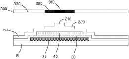
As shown in fig. 1d, a second insulating buffer layer 50 covering the metal oxide layer 40 is formed on the first insulating buffer layer 30, and a first photoresist pattern 210 and a second photoresist pattern 220 are formed on the second insulating buffer layer 50, wherein the first photoresist pattern 210 and the second photoresist pattern 220 are correspondingly located on the metal oxide layer 40, and the thickness of the first photoresist pattern 210 is greater than that of the second photoresist pattern 220.
Specifically, the method of forming the first and second photoresist patterns 210 and 220 includes: a photoresist layer is coated on the second insulating buffer layer 50, and the photoresist layer is exposed and developed using a half-tone mask 300(half-tone mask) so that the first photoresist pattern 210 and the second photoresist pattern 220 are left on the photoresist layer, and the second insulating buffer layer 50 is exposed in other regions where no photoresist is left.
The half-tone mask 300 includes an opaque region 310, a semi-opaque region 320, and a full-opaque region 330, wherein the opaque region 310, the semi-opaque region 320, and the full-opaque region 330 correspond to the first photoresist pattern 210, the second photoresist pattern 220, and a region where no photoresist is to be left, respectively. After exposure and development, the photoresist layer only leaves the first photoresist pattern 210 and the second photoresist pattern 220, and the thickness of the first photoresist pattern 210 is greater than that of the second photoresist pattern 220.
The material of the second insulating buffer layer 50 may be silicon nitride (SiN) x ) Silicon oxide (SiO) x ) Silicon oxynitride (SiO) x N y ) Aluminum oxide (AlO) x ) Etc. or silicon oxide (SiO) x ) Silicon oxynitride (SiO) x N y ) Aluminum oxide (AlO) x ) And silicon nitride (SiN) x ) A plurality of them are combined to form a multilayer composite material.
As shown in fig. 1e, the second insulating buffer layer 50, the first photoresist pattern 210 and the second photoresist pattern 220 are etched, and the first photoresist pattern 210, the exposed second insulating buffer layer 50 (i.e. the portion not covered by the first photoresist pattern 210 and the second photoresist pattern 220) and the portion of the second insulating buffer layer 50 under the first photoresist pattern 210 are removed, so that the second insulating buffer layer 50 under the first photoresist pattern 210 and the second photoresist pattern 220 form a first insulating pattern 51 and a second insulating pattern 52 with different thicknesses after etching, wherein the thickness of the second insulating pattern 52 is less than that of the first insulating pattern 51.
Since the thickness of the first photoresist pattern 210 is greater than that of the second photoresist pattern 220, the first photoresist pattern 210 is thinned during the etching process, the first insulation pattern 51 remains the original thickness under the protection of the first photoresist pattern 210, and the second insulation buffer layer 50 under the second photoresist pattern 220 is continuously etched and thinned after the second photoresist pattern 220 is completely etched, so that the thickness of the second insulation pattern 52 is less than that of the first insulation pattern 51.
As shown in fig. 1f, the first photoresist pattern 210 over the first insulating pattern 51 is removed.
As shown in fig. 1g, the metal oxide layer 40 is ion-doped using the first insulating pattern 51 and the second insulating pattern 52 as a mask, so that a region of the metal oxide layer 40 not shielded by the first insulating pattern 51 and the second insulating pattern 52 is converted from a semiconductor to a conductor to form a first conductor region 41.
As shown in fig. 1h, a second metal layer is formed and is patterned by etching, such that the second metal layer forms a source electrode 61, a drain electrode 62 and a gate electrode 63 which are spaced apart from each other, wherein the source electrode 61 and the drain electrode 62 are both connected in contact with the first conductor region 41 of the metal oxide layer 40, and the gate electrode 63 is disposed above the first insulation pattern 51.
Furthermore, a data line 64 is formed when the second metal layer is etched and patterned, and the data line 64 is electrically connected with the source electrode 61.
In the embodiment, the halftone mask 300 is used to complete the patterning of the first insulating pattern 51 and the second insulating pattern 52 with different thicknesses, the first insulating pattern 51 and the second insulating pattern 52 with different thicknesses are used to dope ions into the metal oxide layer 40, and protect the metal oxide layer 40 when forming the source electrode 61, the drain electrode 62, and the gate electrode 63, and the whole process does not need to use multiple masks, thereby saving the process steps, reducing the manufacturing cost, and improving the production efficiency.
As shown in fig. 1i, the second insulating pattern 52 is etched and removed by using the source electrode 61, the drain electrode 62 and the gate electrode 63 as a mask, so that a portion of the metal oxide layer 40 under the second insulating pattern 52 is exposed, and the gate insulating layer 53 is formed by remaining the first insulating pattern 51.
As shown in fig. 1j, the exposed portion of the metal oxide layer 40 is ion-doped to be converted into a conductor, thereby forming a second conductor region 42. The portion of the metal oxide layer 40 that is not conductor-ized under the first insulating pattern 51 forms a semiconductor region 43 (i.e., an active layer) of the metal oxide thin film transistor.
The first conductor region 41 and the second conductor region 42 formed by the metal oxide layer 4 by the conductor formation have a function similar to a Lightly Doped Drain (LDD), that is, a low Doped Drain region is disposed near the Drain in the channel of the active layer, and the low Doped Drain region is also subjected to a partial voltage to weaken the electric field of the Drain, thereby preventing the hot electron degradation effect.
The preferred embodiment of the present invention further provides a metal oxide thin film transistor, which is formed by the above method for manufacturing a metal oxide thin film transistor, as shown in fig. 1j, the metal oxide thin film transistor includes:
a substrate 10;
a first insulating buffer layer 30 on the substrate 10;
a metal oxide layer 40 on the first insulating buffer layer 30, the metal oxide layer 40 having a first conductor region 41, a second conductor region 42, and a semiconductor region 43;
a gate insulating layer 53 on the semiconductor region 43; and
and a source electrode 61, a drain electrode 62 and a gate electrode 63 formed at the same layer and spaced apart from each other, wherein the gate electrode 63 is disposed on the gate insulating layer 53, the source electrode 61 and the drain electrode 62 are covered on the first conductor region 41 and are in contact with the first conductor region 41, and the second conductor region 42 is exposed between the source electrode 61, the drain electrode 62 and the gate insulating layer 53 (gate electrode 63).
Further, the metal oxide thin film transistor further includes a shielding layer 21 and a scanning line 22 formed on the same layer and spaced apart from each other, and the shielding layer 21 and the scanning line 22 are disposed on the substrate 10 and under the first insulating buffer layer 30, i.e., between the substrate 10 and the first insulating buffer layer 30.
As shown in fig. 4, in the method for fabricating the metal oxide thin film transistor, after removing the first photoresist pattern 210 located above the first insulating pattern 51, patterning the first insulating pattern 51 and the first insulating protection layer 30 to form a first through hole 501 to expose the scan line 22, and when forming the gate electrode 63, the gate electrode 63 is filled in the first through hole 501 to be in contact with the scan line 22. Namely, the first insulating buffer layer 30 and the gate insulating layer 53 of the metal oxide thin film transistor are provided with a first through hole 501 exposing the scanning line 22, and the gate electrode 63 is filled in the first through hole 501 and is connected with the scanning line 22 in a contact manner.
Further, the metal oxide thin film transistor further includes a data line 64 connected to the source electrode 61, and the data line 64 is formed in the same layer as the source electrode 61, the drain electrode 62, and the gate electrode 63.
The metal oxide thin film transistor manufactured by the method can be used as an array substrate in a Liquid Crystal Display (LCD) panel, and can also be used as an array substrate in an Organic Light Emitting Diode (OLED) panel.
The invention also provides an array substrate, and a plurality of metal oxide thin film transistors which are arranged in an array manner are arranged on the array substrate. FIG. 2 is a schematic plan view of a partial structure of an array substrate according to a preferred embodiment of the invention; FIG. 3 is a schematic cross-sectional view taken along line A-A of FIG. 2; fig. 4 is a schematic cross-sectional view taken along line B-B of fig. 2. Referring to fig. 2, fig. 3 and fig. 4, when the array substrate is applied to a liquid crystal display panel, the array substrate further includes:
a first passivation layer 70 covering the source electrode 61, the drain electrode 62, the gate electrode 63, and the data line 64;
a planarization layer 80 covering the first passivation layer 70;
a common electrode 91 on the planarization layer 80 and formed of the first transparent conductive layer by etching patterning;
a second passivation layer 100 covering the common electrode 91;
and a pixel electrode 110 formed on the second passivation layer 100 and patterned by etching from the second transparent conductive layer, wherein a contact hole 101 is formed in the second passivation layer 100, the planarization layer 80, and the first passivation layer 70 at a position corresponding to the drain electrode 62, and the pixel electrode 110 is filled in the contact hole 101 and is electrically connected to the drain electrode 62.
It is understood that when the metal oxide thin film transistor is applied to an array substrate in an organic light emitting diode panel, the pixel electrode 110 is an anode of the light emitting diode. The shielding layer 21 can connect the electrical signal more stably, and the signal is connected to the source electrode 61, so that the driving current is more easily saturated, and the organic light emitting diode is more suitable for being driven.
The array substrate with the metal oxide thin film transistor can be matched with active driving devices of various displays, so that the product is diversified, and the added value of the product is improved.
The metal oxide thin film transistor, the manufacturing method thereof and the array substrate provided by the embodiment of the invention have the following beneficial effects:
1. the semiconductor region 43 for forming the active layer in the metal oxide layer 40 is always protected by the first and second insulating buffer layers 30 and 50 during the fabrication process, and the semiconductor region 43 is not damaged by the process, so that the performance of the metal oxide thin film transistor is excellent.
2. The metal oxide layer 40 is made of two conductor layers, so that the characteristics of the metal oxide thin film transistor can be adjusted flexibly, and the metal oxide thin film transistor can be used with different purposes.
3. The metal oxide structure is skillfully conducted by using the halftone mask 300, so that a metal oxide thin film transistor with a top gate framework is formed, and the gate 63, the source 61 and the drain 62 are manufactured in the same layer, so that the efficiency is higher.
4. The invention has simple process, can be fused with the existing process, has high implementation and is easy to realize mass production.
The metal oxide thin film transistor, the manufacturing method thereof and the array substrate provided by the invention are described in detail, and the principle and the implementation mode of the invention are explained by applying specific examples, and the description of the examples is only used for helping to understand the method and the core idea of the invention; meanwhile, for a person skilled in the art, according to the idea of the present invention, there may be variations in the specific embodiments and the application scope, and in summary, the content of the present specification should not be construed as a limitation to the present invention.