Disclosure of Invention
The application provides a device verification method, device and system, which are used for performing security verification on PCIE devices, realizing the secure start of the PCIE devices and ensuring the security and credibility of electronic devices.
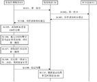
In a first aspect, an embodiment of the present application provides a device verification method applied to an electronic device, where the electronic device includes a processing module and a device management module, and the method includes:
the device management module acquires a firmware of the PCIE device interconnected by the rapid peripheral component assembly;
the equipment management module verifies the firmware;
if the verification is passed, the equipment management module sends a first verification result to the processing module; the first verification result is used for indicating the processing module to allocate Peripheral Component Interconnect (PCI) resources to the PCIE equipment, and the PCI resources are resources applied to the processing module by the PCIE equipment.
In the method, the device management module may acquire the firmware of the PCIE device, verify the firmware, and send the verification result to the processing module. When the verification is passed, the processing module allocates PCI resources to the PCIE equipment; and when the verification fails, the processing module does not allocate the PCI resources to the PCIE equipment. By the method, the PCIE equipment can be safely started, so that the safety and the credibility of the whole electronic equipment are ensured.
In a possible implementation manner, if the verification fails, the device management module sends a second verification result to the processing module, where the second verification result is further used to indicate that the processing module controls the PCIE device to be in a power-down state or a reset state.
In the method, when the verification fails, the processing module may further control the PCIE device to be in a power-down state or a reset state, so that the influence of the unsafe PCIE device on the electronic setting may be more thoroughly eliminated. Wherein, the power-down state can also be called a power-off state (the current is 0) or a sleep state (the current is lower than the threshold); the reset state may also be referred to as a default state or an initial state.
In a possible implementation manner, the acquiring, by the device management module, firmware of a PCIE device interconnected by a Peripheral Component Interconnect Express (PCIE) module includes:
the device management module sends a first instruction to the processing module, wherein the first instruction is used for acquiring a firmware of the PCIE device;
the device management module receives the firmware of the PCIE device sent by the processing module, where the firmware is acquired by the processing module from the PCIE device based on the first instruction.
In the method, the device management module may send a first instruction for acquiring the firmware of the PCIE device to the processing module. The processing module may acquire the firmware of the PCIE device from the PCIE device according to the first instruction, and forward the firmware of the PCIE device to the device management module. By the method, the device management module can acquire the firmware of the PCIE device so as to conveniently perform security verification on the firmware of the PCIE device.
In a possible implementation manner, the acquiring, by the device management module, firmware of a PCIE device interconnected by a Peripheral Component Interconnect Express (PCIE) module includes:
the device management module sends a second instruction to the PCIE device, where the second instruction is used to acquire a firmware of the PCIE device;
the device management module receives the firmware of the PCIE device sent by the PCIE device.
In the method, the device management module can directly acquire the firmware of the PCIE device from the PCIE device, so that the device management module can quickly acquire the firmware of the PCIE device. In a possible implementation manner, the device management module decrypts the digital signature based on a pre-stored public key, and previously includes:
the device management module acquires a public key of the PCIE device.
In the method, the device management module can obtain the public key of the PCIE device, so that the device management module can perform security verification on the firmware of the PCIE device.
In a possible implementation manner, the sending, by the device management module, the first verification result to the processing module includes:
the equipment management module sends equipment information of the PCIE equipment to the processing module;
the device management module receives a query request sent by the processing module, wherein the query request is used for acquiring a verification result of the PCIE device;
the device management module sends a first verification result to the processing module.
In the method, the equipment management module can send the verification result to the processing module in a request and response mode, so that the safe sending of the verification result is realized.
In one possible implementation, the PCI resources include one or more of a memory space, a bus/device/function BDF.
In the above method, the PCI resources may make PCIE devices available in the operating system.
In a possible implementation manner, the communication interface between the device management module and the PCIE device is a system management bus SMBus interface or a network controller sideband NC-SI interface.
In the method, an SMBus interface or an NC-SI interface may be provided between the device management module and the PCIE device, so that the device management module may directly communicate with the PCIE device.
In one possible embodiment, the first instruction is a platform-level data model, PLDM, message.
In the method, the device management module may obtain the firmware of the PCIE device through the first instruction, so as to perform security verification on the firmware of the PCIE device.
In a second aspect, an embodiment of the present application provides a computing device, including: one or more processors, one or more memories, a device manager; the one or more processors are coupled with the one or more memories and the device manager, respectively; the one or more memories for storing computer program code, the computer program code comprising computer instructions; the computer instructions, when executed on the device manager, cause the device manager to perform the method of any of the first aspects.
The device manager in the computing device may obtain the firmware of the PCIE device, verify the firmware, and send a verification result to the processor in the computing device. When the verification is passed, the processor allocates PCI resources to the PCIE equipment; when the verification fails, the processor does not allocate PCI resources to the PCIE device. By the method, the PCIE equipment can be safely started, so that the safety and the credibility of the whole computing equipment are ensured.
In a third aspect, an embodiment of the present application provides a device management system, including an electronic device and a PCIE device, where,
the electronic device is configured to execute the method described in any of the first aspect to confirm a verification result of the firmware in the PCIE device.
The electronic device can acquire the firmware of the PCIE device and verify the firmware. When the verification passes, the electronic equipment allocates PCI resources to the PCIE equipment; and when the verification fails, the electronic device does not allocate the PCI resources to the PCIE device. By the method, the PCIE equipment can be safely started, so that the safety and the credibility of the whole electronic equipment are ensured.
In a fourth aspect, an embodiment of the present application provides a chip, where the chip is configured to perform: acquiring a firmware of the PCIE equipment interconnected with the fast peripheral component assembly; verifying the firmware; and if the verification is passed, sending a first verification result.
In some embodiments, the first verification result is used to indicate that peripheral component interconnect PCI resources are allocated to the PCIE device, and optionally, the PCI resources include one or more of a memory space, a bus/device/function BDF.
In some embodiments, if the verification fails, the device management module sends a second verification result, and the second verification result is further used to instruct to control the PCIE device to be in a power-down state or a reset state.
Wherein the chip may perform the method of any of the first aspect.
The chip can acquire the firmware of the PCIE equipment and verify the firmware of the PCIE equipment according to a pre-stored public key of the PCIE equipment, so that the integrity and the legality of the firmware of the PCIE equipment are ensured.
In a fifth aspect, an embodiment of the present application provides a computer-readable storage medium, where computer-executable instructions are stored, and when a processor executes the computer-executable instructions, the apparatus authentication method according to any one of the first aspects is implemented.
Detailed Description
Reference will now be made in detail to the exemplary embodiments, examples of which are illustrated in the accompanying drawings. When the following description refers to the accompanying drawings, like numbers in different drawings represent the same or similar elements unless otherwise indicated. The embodiments described in the following exemplary embodiments do not represent all embodiments consistent with the present application. Rather, they are merely examples of apparatus and methods consistent with certain aspects of the application, as detailed in the appended claims.
It should be noted that, in this document, the terms "comprises," "comprising," or any other variation thereof, are intended to cover a non-exclusive inclusion, such that a process, method, article, or apparatus that comprises a list of elements does not include only those elements but may include other elements not expressly listed or inherent to such process, method, article, or apparatus. Without further limitation, an element defined by the phrase "comprising an … …" does not exclude the presence of other like elements in a process, method, article, or apparatus that comprises the element.
To facilitate an understanding of the present application, a description will first be made of concepts related to the present application.
Firmware: firmware is code that runs on a device chip to implement device functions. For example, the firmware of the PCIE device is a code running on a PCIE device chip, and the firmware of the PCIE device is used to implement the function of the PCIE device. For example, if the PCIE device is a network card, the firmware of the PCIE device may be used to implement functions of network connection, message transceiving, protocol offloading, and the like of the network card.
Digital signature: a character string that cannot be forged by others is generated for the information sender. The digital signature may verify the integrity and authenticity of the information sent by the sender of the information. The method for generating the digital signature can be referred to the related art, and is not described in detail herein.
Public key: is the public part of the key pair used with the private key. Public keys are typically used to encrypt data, verify digital signatures, and the like. In this application, the public key and the private key are a key pair in an asymmetric cryptographic algorithm, the private key refers to a key used by the PCIE device to generate a digital signature, and the public key refers to a key used to verify the digital signature of the PCIE device.
For ease of understanding, the device authentication system architecture according to the embodiment of the present application is first described with reference to fig. 1 to 2.
Fig. 1 is a schematic architecture diagram of a device verification system according to an embodiment of the present application. As shown in fig. 1, the device authentication system includes: electronic device 100 and PCIE device 101. The electronic device 100 and the PCIE device 101 are connected based on a wired or wireless connection, and the electronic device 100 provides an operation resource for the PCIE device 101, so that the PCIE device 101 executes its corresponding function. Wherein,
the electronic device 100 includes, but is not limited to, a server cluster, a laptop computer, a desktop computer, a mobile phone, a smartphone, a tablet, a multimedia player, an e-reader, a smart car device, a smart appliance, an artificial intelligence device, a wearable device, an internet of things device, or a virtual reality/augmented reality/mixed reality device, etc.
The PCIE device 101 includes, but is not limited to, a network card, a RAID (redundant array of independent disks) card, a video card, a Peripheral Component Interconnect (PCI) Solid State Drive (SSD) card, an accelerator card, and the like. It should be understood that the number of PCIE devices 101 may be one or more, and is not limited in this embodiment of the application.
The electronic device 100 may include a processing module 102 and a device management module 103. The processing module 102 may include a Basic Input Output System (BIOS) 104, a processor 105.
Processor 105 may include one or more processing units, such as: the processor 105 may include an Application Processor (AP), a modem processor, a Graphics Processing Unit (GPU), an Image Signal Processor (ISP), a controller, a memory, a video codec, a Digital Signal Processor (DSP), a baseband processor, and/or a neural-Network Processing Unit (NPU), among others. The different processing units may be separate devices or may be integrated into one or more processors.
The BIOS104 is boot software for the processor 105, and may complete initialization of the processor 105.
The device management module 103 may also be referred to as a server processor or a Baseboard Management Controller (BMC), the device management module 103 operates independent of the processor 105, the BIOS104, or the operating system of the electronic device 100, and the device management module 103 has its own firmware, power supply, MAC address, and network interface. In some embodiments, device management module 103 performs component management, asset management tasks in electronic device 100. Such as power-up and power-down control, fan speed regulation, electronic tag management. Alternatively, the device management module 103 may be mounted on a chip, which is generally referred to as an out-of-band management chip.
During the startup of the electronic device 100, it is necessary to perform security authentication on each module mounted on the electronic device 100 and the PCIE device 101 connected to the electronic device 100. The module and the PCIE device 101 that pass the authentication can operate normally in the electronic device 100. Modules and PCIE devices 101 that fail to be verified can be shielded by the electronic device 100 and cannot operate normally. The security verification can ensure the integrity and validity of the modules running in the electronic device 100, thereby ensuring the safety and reliability of the electronic device 100.
It is to be understood that the illustrated structure of the embodiment of the present application does not specifically limit the electronic device 100. In other embodiments of the present application, electronic device 100 may include more or fewer components than shown, or some components may be combined, some components may be split, or a different arrangement of components. The illustrated components may be implemented in hardware, software, or a combination of software and hardware.
In some embodiments, as shown in fig. 2, fig. 2 is a schematic structural diagram of another device authentication system provided in the embodiments of the present application. Referring to fig. 2, the electronic device 100 includes a processing module 102 and a device management module 103. The processing module 102 may include a processor 105, a BIOS104, and a bridge 106. Optionally, the processing module 102 may further include a Read Only Memory (ROM) and a Random Access Memory (RAM). ROM may also be referred to as fixed memory. The ROM can only read information and cannot write information. Typically, the BIOS104 is solidified in ROM on the motherboard of the electronic device 100. The RAM is an internal memory that exchanges data directly with the processor 105. Wherein,
the bridge chip 106 is a processing chip that performs data and instruction exchanges directly with the processor 105, serving as a connection bridge. For example, the bridge piece 106 may be a connection bridge between the processor 105 and the device management module 103. Optionally, the bridge 106 may be a south bridge chip and/or a north bridge chip.
The device management module 103 may be coupled to (in communication with) the processor 105 via the bridge piece 106. Optionally, a mouse 107, keyboard 108, or the like may be coupled to (in communication with) the processor 105 via the bridge 106.
Next, 3 methods for performing security verification on each module running on the electronic device 100 and the PCIE device 101 during the startup phase are exemplarily shown in the following:
method 1, device management module 103 performs security verification on system fixed components of electronic device 100. For example, the system fixed components of the electronic device 100 may be the BIOS104, the device management module 103.
Method 2, the PCIE device 101 performs security verification on itself.
Method 3, a Unified Extensible Firmware Interface (UEFI) BIOS performs security verification on the UEFI driver in the Firmware of the PCIE device 101.
Next, the method 1 is described with reference to fig. 3, taking as an example that the device management module 103 performs security authentication on the BIOS.
Fig. 3 is a schematic diagram illustrating the device management module 103 performing security authentication on the BIOS 104. Referring to fig. 3, a Root of Trust (RoT) of the system is stored in the device management module 103.
RoT is a trusted module in a trusted computing system within electronic device 100, and is a trusted source based on cryptography and hardware protection, which is used as a starting point to establish a trust chain of the system. The public key of the BIOS104 is stored in the RoT, so that the RoT performs secure verification on the BIOS firmware based on the public key of the BIOS 104.
In the process of verifying the electronic device, the electronic device 100 sequentially runs the modules, and in the process of initializing the BIOS104, the device management module 103 obtains the BIOS firmware. The BIOS firmware includes firmware code and a digital signature. Device management module 103 may verify the digital signature with the public key of BIOS 104. If the verification passes, the BIOS104 may continue to boot; if the verification fails, the BIOS104 stops running, so that the secure boot of the BIOS104 can be realized. However, the above security authentication method does not support security authentication of the PCIE device 101, that is, the PCIE device 101 cannot be securely authenticated by the above method. Therefore, the security authentication method cannot ensure the integrity and the validity of the PCIE device 101, and thus cannot ensure the security and the credibility of the electronic device 100.
Next, the above method 2 will be described with reference to fig. 4A to 4B.
Fig. 4A is a schematic diagram of a PCIE device 101 performing security authentication on itself. Referring to fig. 4A, the processing module 102 and the PCIE device 101 may communicate through a PCIE interface. The chip of the PCIE device 101 stores RoT. The chip of the PCIE device 101 also stores the firmware of the PCIE device 101. The firmware of PCIE device 101 includes firmware code and digital signatures. The RoT stores therein the public key of the PCIE device 101.
In the verification process of the PCIE device 101, the RoT may verify the digital signature of the PCIE device 101 firmware through the public key of the PCIE device 101.
Fig. 4B is a schematic diagram of another PCIE device 101 performing security authentication on itself. Referring to fig. 4B, the processing module 102 and the PCIE device 101 may communicate through a PCIE interface. The chip of the PCIE device 101 stores firmware of the PCIE device 101. The firmware of PCIE device 101 includes firmware code and digital signatures. The firmware of the PCIE device 101 also includes RoT. The RoT stores therein the public key of the PCIE device 101.
In the verification process of the PCIE device 101, the RoT may verify the digital signature of the PCIE device 101 firmware through the public key of the PCIE device 101.
The security verification method described in fig. 4A-4B can defend against far-end network attacks, and ensure that PCIE firmware is not tampered, but the security verification method cannot defend against near-end attacks. For example, a storage carrier replacing RoT, or a PCIE device 101. Therefore, the security authentication method of PCIE cannot guarantee the security and the credibility of the electronic device 100.
Next, the method 3 will be described with reference to fig. 5.
Fig. 5 is a schematic diagram of UEFI BIOS performing security verification on UEFI drivers in the firmware of PCIE device 101. Referring to FIG. 5, the UEFI BIOS may run on ROM or RAM. The UEFI BIOS stores the public key of the PCIE device 101. PCIE device 101 includes firmware for PCIE device 101. The firmware of PCIE device 101 includes UEFI drivers and firmware code. The UEFI driver includes a digital signature of the UEFI driver.
At the stage of enumerating the PCIE device 101, the UEFI BIOS may load the UEFI driver of the PCIE device 101 through the processing module 102, and perform security verification on the digital signature in the UEFI driver by using the public key of the PCIE device 101. The safety verification method can verify the integrity of the UEFI driver of the PCIE device 101 to ensure that the UEFI driver is not tampered, but does not perform safety verification on the entire firmware of the PCIE device 101, and cannot ensure the integrity of the entire firmware of the PCIE device 101.
In order to solve the technical problems in the foregoing multiple security verification methods, embodiments of the present application provide an apparatus verification method to implement secure startup of PCIE device 101. As shown in fig. 6, fig. 6 is a schematic diagram of a method for security authentication of a PCIE device 101 according to the embodiment of the present application.
Referring to fig. 6, the processing module 102 may communicate with the PCIE device 101, and the processing module 102 may also communicate with the device management module 103. The device management module 103 may store a public key of the PCIE device 101. In the verification process of the electronic device 100, the device management module 103 may obtain the firmware of the PCIE device 101, and perform security verification on the firmware of the PCIE device 101 through the public key of the PCIE device 101. If the verification is passed, the processing module 102 of the electronic device 100 allocates a Peripheral Component Interconnect (PCI) resource to the PCIE device 101, so that the PCIE device 101 may be available in an Operating System (OS) of the electronic device 100. If the verification fails, the processing module 102 of the electronic device 100 shields the PCIE device 101. By the method, the secure startup of the PCIE equipment 101 is realized, so that the security and the credibility of the whole computer system are ensured.
The technical solution of the present application will be described in detail below with specific examples. The following several specific embodiments may be combined with each other, and details of the same or similar concepts or processes may not be repeated in some embodiments.
Fig. 7 is a flowchart illustrating a device verification method according to an embodiment of the present application. Referring to fig. 7, the method may include:
s701, the device management module 103 of the electronic device 100 obtains the firmware of the PCIE device 101.
The PCIE device 101 may be a PCIE device 101 that is connected to the electronic device 100 via a wired or wireless connection.
The device management module 103 can obtain the firmware of the PCIE device 101 from the PCIE device 101.
Firmware code and digital signatures are included in the firmware of PCIE device 101.
The digital signature is obtained by encrypting the first digest based on a private key of the PCIE device 101; the first abstract is obtained by calculating the firmware code based on a preset algorithm.
Illustratively, the predetermined algorithm may be a hash algorithm. The PCIE device 101 may calculate the firmware code of itself through a hash algorithm to obtain a first digest, and encrypt the first digest through a private key of itself to obtain a digital signature.
S702, the device management module 103 verifies the firmware.
The device management module 103 may verify the firmware by: the device management module 103 decrypts the digital signature based on a pre-stored public key of the PCIE device 101 to obtain a first digest; the device management module 103 calculates the firmware code through a preset algorithm to obtain a second abstract; if the first abstract is the same as the second abstract, determining that the verification is passed; and if the first abstract is different from the second abstract, determining that the verification is not passed.
The first digest is obtained by calculating the firmware code of the PCIE device 101 through a preset algorithm. The PCIE device 101 may further encrypt the first digest by using a private key to obtain a digital signature. Accordingly, the device management module 103 may decrypt the digital signature using the public key to obtain the first digest.
The second digest is a digest obtained by the device management module 103 calculating the firmware code of the PCIE device 101 through the same preset algorithm. Before verifying the firmware, the device management module 103 may obtain a public key of the PCIE device 101. The public key of the PCIE device 101 may be stored in the device management module 103, or the public key of the PCIE device 101 may also be stored in a module other than the device management module 103. For different storage locations of the public key of the PCIE device 101, the device management module 103 may obtain the public key of the PCIE device 101 in the following two ways:
in the first mode, the device management module 103 obtains the pre-stored public key from the local.
The device management module 103 may store a public key of at least one PCIE device 101 in advance. After the device management module 103 acquires the firmware of the PCIE device 101, the device management module 103 may read the device information of the PCIE device 101 from the firmware, and locally acquire the public key corresponding to the PCIE device 101 according to the device information. For example, the device information of the PCIE device 101 includes manufacturer information of the PCIE device 101, a device identifier (e.g., Serial Number (SN)), a preset identifier, and the like.
In this implementation manner, the device management module 103 can acquire the public key of the PCIE device 101 more quickly, and thus, the fast security verification of the PCIE device 101 is implemented.
In a second manner, the device management module 103 may obtain the public key of the PCIE device 101 from a module other than the device management module 103.
For example, modules other than the device management module 103 may be dedicated security chips. That is, the public key of at least one PCIE device 101 may be stored in the dedicated security chip.
In this way, the device management module 103 obtains the public key of the PCIE device 101 in at least 3 cases as follows:
in case 1, after acquiring the firmware, the device management module 103 acquires the specified public key from the dedicated security chip.
After the device management module 103 obtains the firmware of the PCIE device 101, the device information of the PCIE device 101 may be read from the firmware, and a public key corresponding to the PCIE device 101 is obtained from the dedicated security chip according to the device information.
In case 2, after the device management module 103 obtains the firmware, all public keys are obtained from the dedicated security chip.
After acquiring the firmware of the first PCIE device 101, the device management module 103 may acquire the public keys corresponding to all the PCIE devices 101 from the dedicated security chip, and store the public keys locally. When a certain PCIE device 101 is verified, the device management module 103 may locally acquire the public key corresponding to the PCIE device 101 through the device information of the PCIE device 101.
In case 3, before the device management module 103 obtains the firmware, all public keys are obtained from the dedicated security chip.
When the electronic device is verified, the dedicated security chip may verify the device management module 103, and import the public keys of all PCIE devices 101 stored in the dedicated security chip into the device management module 103. After the device management module 103 obtains the public key of the PCIE device 101, security verification may be performed on the PCIE device 101.
In this implementation manner, the device management module 103 may obtain the public key of the PCIE device 101 from another module, so that the storage resource of the device management module 103 is saved.
S703, the device management module 103 determines whether the verification is passed.
If yes, go to step S704.
If not, go to S705.
S704, the device management module 103 sends the first verification result to the processing module 102.
The first verification result is used to instruct the processing module 102 to allocate a peripheral component interconnect PCI resource to the PCIE device 101, where the PCI resource is a resource applied to the processing module 102 by the PCIE device 101. PCI resources may include one or more of a Bus Device Function (BDF), a memory space.
The BDF is a unique identifier for identifying each function of the PCIE device 101 under the PCIE bus.
A Low Pin Count (LPC) interface may be set between the device management module 103 and the processing module 102, and the device management module 103 may send the first verification result to the processing module 102 through the LPC interface.
In a possible implementation manner, after the device management module 103 verifies the firmware, the first verification result may be directly sent to the processing module 102.
In another possible implementation manner, the device management module 103 may send the first verification result to the processing module 102 by requesting a response. As shown in fig. 8, fig. 8 is a schematic diagram that the device management module 103 sends a first verification result to the processing module 102 by requesting a response according to the embodiment of the present application.
Referring to fig. 8, after the device management module 103 verifies the firmware, the device information of the PCIE device 101 may be sent to the processing module 102. The device information may include slot number information of PCIE device 101. The processing module 102 may send an acquisition request of an authentication result of the PCIE device 101 to the device management module 103 according to the device information of the PCIE device 101. After receiving the acquisition request, the device management module 103 may send the verification result of the PCIE device 101 to the processing module 102.
S705, the device management module 103 sends the second verification result to the processing module 102.
The second verification result is used to instruct the processing module 102 not to allocate PCI resources to the PCIE device 101; or, the second verification result is used to instruct the processing module 102 to control the PCIE device 101 to be in a power-down state or a reset state.
The method for the device management module 103 to send the second verification result to the processing module 102 is the same as the method for the device management module 103 to send the first verification result to the processing module 102, which may specifically refer to S704, and is not described herein again.
S706, the processing module 102 configures the PCIE device 101 according to the first verification result/the second verification result.
In the embodiment of the present application, the BIOS104 is a system running on the processing module 102. The device management module 103 may transmit the first verification result/the second verification result to the processing module 102, or the device management module 103 may transmit the first verification result/the second verification result to the BIOS104 in the processing module 102. Similarly, the processing module 102 may configure the PCIE device 101 according to the first verification result/the second verification result, or the BIOS104 in the processing module 102 may configure the PCIE device 101 according to the first verification result/the second verification result. When the processing module 102 receives the first verification result, that is, the firmware of the PCIE device 101 has integrity and validity, the processing module 102 allocates PCI resources to the PCIE device 101, so that the PCIE device 101 can be available in the OS. For example, the processing module 102 may allocate Bus Device Function (BDF) resources for the PCIE Device 101; or the processing module 102 may allocate a memory space for the PCIE device 101.
When the processing module 102 receives the second verification result, that is, the firmware of the PCIE device 101 does not have integrity and validity, the processing module 102 may shield the PCIE device 101, so that the PCIE device 101 is not available in the OS. The processing module 102 can shield the PCIE device authentication at least in the following 3 ways:
in the mode 1, the processing module 102 does not allocate PCI resources to the PCIE device 101.
In the mode 2, the processing module 102 controls the PCIE device 101 to be in a power-down state.
For example, in the electronic device 100 supporting hot-plug of the PCIE device 101, the electronic device 100 may individually control the power supply circuit of the PCIE device 101. When the processing module 102 receives the second verification result, the processing module 102 may notify the hardware control module, so that the hardware control module controls the PCIE device 101 to be in a power-down state.
In the mode 3, the processing module 102 controls the PCIE device 101 to be in a reset state.
When the processing module 102 receives the second verification result, the processing module 102 may output a reset signal to the PCIE device 101, so that the PCIE device 101 is in a reset state. In some embodiments, the reset state may be understood as an initial default state.
In the device verification method provided in this embodiment, the device management module 103 may obtain the firmware of the PCIE device 101 and the public key of the PCIE device 101. The device management module 103 may also verify the digital signature in the firmware and send the first/second verification result to the processing module 102. When receiving the first verification result, the processing module 102 allocates PCI resources to the PCIE device 101; when receiving the second verification result, the processing module 102 may shield the PCIE device 101. By the method, the secure start of the PCIE device 101 can be realized, so that the security and the credibility of the whole electronic device 100 are ensured.
Compared with the mode that another security chip is arranged to verify the PCIE equipment, the embodiment of the application saves a special security chip, has lower arrangement cost and simpler hardware scheme of the electronic equipment. Compared with a mode of verifying the PCIE device through the BIOS, the verification subject is unified, that is, the device management module 103 performs security verification on other modules, because the device management module 103 performs security verification on the BIOS in the existing scheme, the problem that the device management module 103 transfers the public key of the PCIE device to the BIOS is avoided, and the scheme complexity and insecurity factors are increased.
On the basis of the embodiment of fig. 7, the device management module 103 can obtain the firmware of the PCIE device 101 through at least the following two methods.
In the method 1, the device management module 103 obtains the firmware of the PCIE device 101 from the PCIE device 101 through the processing module 102.
As shown in fig. 9, fig. 9 is a schematic diagram that a device management module 103 obtains a firmware of a PCIE device 101 through a processing module 102 according to the embodiment of the present application. Referring to fig. 9, the device management module 103 includes device management module 103 firmware. The device management module 103 stores a public key of the PCIE device 101. PCIE device 101 includes PCIE firmware. The firmware of PCIE device 101 includes a digital signature. A first PCIE interface and an LPC interface are arranged between the device management module 103 and the processing module 102. A second PCIE interface is disposed between the processing module 102 and the PCIE device 101. The device management module 103 may send a firmware acquisition instruction to the processing module 102 through the first PCIE interface. The processing module 102 may acquire the firmware of the PCIE device 101 from the PCIE device 101 through the second PCIE interface according to the firmware acquisition instruction, and forward the firmware of the PCIE device 101 to the device management module 103 through the first PCIE interface, so that the device management module 103 acquires the firmware of the PCIE device 101.
In the method 2, the device management module 103 acquires the firmware of the PCIE device 101 from the PCIE device 101 through an interface between the device management module 103 and the PCIE device 101.
As shown in fig. 10, fig. 10 is a schematic diagram that a device management module 103 obtains a firmware of a PCIE device 101 through an interface between the device management module 103 and the PCIE device 101 according to the embodiment of the present application. Referring to fig. 10, the device management module 103 includes device management module 103 firmware. The device management module 103 stores a public key of the PCIE device 101. PCIE device 101 includes PCIE firmware. The firmware of the PCIE device 101 includes a digital signature. An LPC interface is provided between the device management module 103 and the processing module 102. A PCIE interface is disposed between the processing module 102 and the PCIE device 101. A System Management Bus (SMBus) interface is arranged between the device Management module 103 and the PCIE device 101; or a Network Controller side band Interface (NC-SI) Interface is arranged between the device management module 103 and the PCIE device 101. The device management module 103 may directly communicate with the PCIE device 101 through the SMBus interface or the NC-SI interface, and acquire the firmware of the PCIE device 101 from the PCIE device 101.
The method 1 will be described below with reference to an example of fig. 11.
Fig. 11 is a flowchart illustrating another device authentication method according to an embodiment of the present application. Referring to fig. 11, the method may include:
s1101, the device management module 103 sends a first instruction to the processing module 102 through the first PCIE interface. The first PCIE interface is a communication interface between the device management module 103 and the processing module 102. The first instruction is a firmware acquisition request message that the device management module 103 requests to acquire the firmware of the PCIE device 101 from the PCIE device 101.
S1102, the processing module 102 forwards the first instruction to the PCIE device 101 through the second PCIE interface.
S1103, the processing module 102 receives, through the second PCIE interface, a firmware acquisition response message, where the firmware acquisition response message includes a firmware of the PCIE device 101, and the firmware of the PCIE device 101 includes a digital signature.
The firmware acquisition response message is a response message sent by the PCIE device 101 for the first instruction.
The second PCIE interface is a communication interface between the processing module 102 and the PCIE device 101.
The first PCIE interface and the second PCIE interface are substantially PCIE interfaces. The PCIE interface carries Management Component Transport Protocol (MCTP) data. The device management module 103 communicates with the PCIE device 101 through the first PCIE interface and the second PCIE interface to implement MCTP communication. The MCTP lower layer supports a physical interface PCIE, a System Management Bus (SMBus), and the like. The MCTP upper layer carries out-of-band management protocol support for a Network Controller Sideband Interface (NC-SI), a Platform Level Data Model (PLDM) and the like. The embodiment of the application adopts a protocol structure of PLDM over MCTP over PCIE. The firmware acquisition request message is a PLDM message; and/or the firmware acquisition response message is a PLDM message.
Original Equipment Manufacturer (OEM) specific data types and command formats are defined in the PLDM specification. The OEM-specific command formats include the command format of a Request (Request) and a Response (Response).
The embodiment of the application utilizes OEM data type of PLDM to extend and define the firmware acquisition request command. As shown in fig. 12, fig. 12 is an OEM PLDM command data format of a firmware acquisition request provided by an embodiment of the present application. Referring to fig. 12, fig. 12 includes a PCIE vendor defined message header, a message code, an MCTP header, a message type, a PLDM header, a PLDM type, PLDM message data, a firmware acquisition request, and a firmware data response.
S1104, the processing module 102 forwards the firmware acquisition response message to the device management module 103 through the first PCIE interface.
In steps S1101-S1104, the processing module 102 forwards the first instruction sent by the device management module 103 to the PCIE device 101. After receiving the firmware acquisition request message, the PCIE device 101 sends the PCIE firmware to the processing module 102. The processing module 102 forwards the PCIE firmware to the device management module 103.
S1105, the device management module 103 obtains the public key of the PCIE device 101.
Please refer to S702, which is not described herein again, for a method for the device management module 103 to obtain the public key of the PCIE device 101.
S1106, the device management module 103 decrypts the digital signature through the public key to obtain the first digest.
S1107, the device management module 103 obtains a second digest corresponding to the firmware.
Please refer to S702, which is not described herein again, for a method for the device management module 103 to obtain the second summary corresponding to the firmware.
S1108, the device management module 103 compares the first abstract with the second abstract to obtain a verification result.
If the first abstract is the same as the second abstract, the verification result of the firmware is verification passing. If the first abstract is not the same as the second abstract, the verification result of the firmware is that the verification is not passed,
s1109, the device management module 103 sends the verification result to the processing module 102.
S1110, the processing module 102 configures the PCIE device 101 according to the verification result.
The embodiments of S1109-S1110 can be seen in S703-S704, which are not described herein.
In the device verification method provided in this embodiment, the device management module 103 obtains the firmware of the PCIE device 101 from the PCIE device 101 through the first PCIE interface and the second PCIE interface, and performs security verification on the firmware. When the verification result is that the verification passes, the processing module 102 allocates a PCI resource to the PCIE device 101; when the verification result is that the verification fails, the processing module 102 may shield the PCIE device 101. By the method, the secure start of the PCIE device 101 can be realized, so that the security and the credibility of the whole electronic device 100 are ensured.
Next, the method 2 will be described with reference to the example of fig. 13.
Fig. 13 is a flowchart illustrating another device verification method according to an embodiment of the present application. Referring to fig. 13, the method may include:
s1301, the device management module 103 sends a second instruction to the PCIE device 101 through an interface between the device management module 103 and the PCIE device 101.
The second instruction is a firmware acquisition request message for acquiring the firmware of the PCIE device 101.
The interface between the device management module 103 and the PCIE device 101 may be at least an SMBus interface or an NC-SI interface.
In one possible implementation manner, an interface between the device management module 103 and the PCIE device 101 is an SMBus interface. The SMBus interface is defined in the interface specification protocol of the PCIE device 101. Almost all PCIE devices 101 support communication over the SMBus interface.
An address resolution protocol is defined in the SMBus specification, and the SMBus address resolution protocol can realize a read-write function through an SMBus device default address '1100001'. As shown in fig. 14, fig. 14 is an SMBus address resolution protocol provided by an embodiment of the present application. Referring to fig. 14, the SMBus address resolution protocol includes an SMBus device default address, a read/write (R/W #) bit completion byte, and a command "0 x 00" to "0 x 1F". "0 x 00", "0 x 05" to "0 x 1F" are reserved command words, and "0 x 01" is an Address Resolution Protocol (ARP) ready command. "0 x 02" and "0 x 03" are General type commands, where "0 x 02" is a reset Device command and "0 x 03" is a Unique Device Identifier (UDID) command to get Device. "0 x 04" is an allocate address command.
In the embodiment of the present application, an SMBus address resolution protocol is used to perform extension, and a Reserved (Reserved) command word is used to define a firmware acquisition command, so as to implement transmission of the firmware of the PCIE device 101. As shown in fig. 15, fig. 15 is a timing sequence of a firmware acquisition command according to an embodiment of the present application. Referring to FIG. 15, the firmware get command timing sequence includes a start bit, a restart bit, an end bit, a read bit, a write bit, an acknowledge bit, a byte count, a message error code, a slave address, a target address, and a firmware get command.
In another possible implementation manner, an interface between the device management module 103 and the PCIE device 101 is an NC-SI interface. The NC-SI interface is mainly used for an Ethernet (Ethernet, Eth) network card, and the other PCIE devices 101 do not support the NC-SI interface. For example, the other PCIE devices 101 may be a Fiber Channel (FC) network card, an InfiniBand (IB) network card, or the like.
The NC-SI specification defines the data format of OEM commands using a media independent interface Transport (RBT) Based interface for transferring NC-SI sideband communication data. The data format of the OEM Command includes the data format of a Command (Command) and a Response (Response). In the embodiment of the application, the OEM command of NC-SI is used for extension, and the firmware acquisition request command is Defined as a Vendor Defined (Vendor Defined) command.
As shown in fig. 16, fig. 16 is an OEM NC-SI command data format for a firmware acquisition request provided by an embodiment of the present application. Referring to fig. 16, the OEM NC-SI command data format of the firmware acquisition request includes a Destination address (MAC, DMAC), a Source address (Source MAC, SMAC), an ethertype, a command header, a control packet type, an Identity identification number (ID) Assigned by an Internet Assigned Number Authority (IANA), a vendor definition command, an acquisition firmware command, a response code, a reason code, and firmware data.
S1302, the PCIE device 101 sends a firmware acquisition response message to the device management module 103 through an interface between the device management module 103 and the PCIE device 101, where the firmware acquisition response message includes a firmware of the PCIE device 101, and the firmware of the PCIE device 101 includes a digital signature.
S1303, the device management module 103 obtains the public key of the PCIE device 101.
S1304, the device management module 103 decrypts the digital signature by using the public key to obtain a first digest.
S1305, the device management module 103 obtains a second digest corresponding to the firmware.
S1306, the device management module 103 compares the first digest with the second digest to obtain a verification result.
S1307, the device management module 103 sends the verification result to the processing module 102.
S1308, the processing module 102 configures the PCIE device 101 according to the verification result.
The implementation of S1303-S1308 may refer to S1105-S1110, which is not described herein.
In the device verification method provided in this embodiment, the device management module 103 may directly communicate with the PCIE device 101, acquire the firmware of the PCIE device 101 from the PCIE device 101, and perform security verification on the firmware. When the verification result is that the verification passes, the processing module 102 allocates a PCI resource to the PCIE device 101; when the verification result is that the verification fails, the processing module 102 may shield the PCIE device 101. By the method, the secure start of the PCIE device 101 can be realized, so that the security and the credibility of the whole electronic device 100 are ensured.
Fig. 17 is a schematic structural diagram of a computing device according to an embodiment of the present application. Referring to fig. 17, the computing device includes: one or more processors 1701, one or more memories 1702, a device manager 1703; the one or more processors 1701 are respectively coupled to the one or more memories 1702 and the device manager 1703; the one or more memories 1702 are for storing computer program code, including computer instructions; when the computer instructions are run on the device manager 1703, the computing device 17 is caused to perform the scheme shown in the device authentication method embodiments described above.
The computing device provided in the embodiment of the present application may execute the scheme shown in the above method embodiment, and the implementation principle and the beneficial effect are similar, which are not described herein again.
The embodiment of the application provides a chip. The chip is used for executing: acquiring firmware of the Peripheral Component Interconnect Express (PCIE) device 101; verifying the firmware; and if the verification is passed, sending a first verification result.
In some embodiments, the first verification result is used to instruct the PCIE device 101 to allocate a peripheral component interconnect PCI resource, where optionally, the PCI resource includes one or more of a memory space, a bus/device/function BDF.
In some embodiments, if the verification fails, the device management module 103 sends a second verification result, where the second verification result is further used to indicate that the PCIE device 101 is controlled to be in a power-down state or a reset state.
The chip may acquire the firmware of the PCIE device 101, and may verify the firmware of the PCIE device 101 according to the pre-stored public key of the PCIE device 101, so as to ensure the integrity and the validity of the firmware of the PCIE device 101.
In some embodiments, the chip may perform the actions performed by the device management module 103 in the device authentication method embodiments described above. The implementation principle and the beneficial effect are similar, and the detailed description is omitted here.
A readable storage medium having a computer program stored thereon; the computer program is for implementing a device authentication method as described in any of the embodiments above.
An embodiment of the present application provides a computer program product, which includes instructions that, when executed, cause a computer to execute the above-mentioned device authentication method. All or a portion of the steps of implementing the above-described method embodiments may be performed by hardware associated with program instructions. The aforementioned program may be stored in a readable memory. When executed, the program performs steps comprising the method embodiments described above; and the aforementioned memory (storage medium) includes: read-only memory (ROM), RAM, flash memory, hard disk, solid state disk, magnetic tape (magnetic tape), floppy disk (flexible disk), optical disk (optical disk), and any combination thereof.
Embodiments of the present application are described with reference to flowchart illustrations and/or block diagrams of methods, apparatus (systems), and computer program products according to embodiments of the application. It will be understood that each flow and/or block of the flow diagrams and/or block diagrams, and combinations of flows and/or blocks in the flow diagrams and/or block diagrams, can be implemented by computer program instructions. These computer program instructions may be provided to a processing unit of a general purpose computer, special purpose computer, embedded processor, or other programmable terminal device to produce a machine, such that the instructions, which execute via the processing unit of the computer or other programmable terminal device, create means for implementing the functions specified in the flowchart flow or flows and/or block diagram block or blocks.
These computer program instructions may also be stored in a computer-readable memory that can direct a computer or other programmable terminal equipment to function in a particular manner, such that the instructions stored in the computer-readable memory produce an article of manufacture including instruction means which implement the function specified in the flowchart flow or flows and/or block diagram block or blocks.
These computer program instructions may also be loaded onto a computer or other programmable terminal device to cause a series of operational steps to be performed on the computer or other programmable apparatus to produce a computer implemented process such that the instructions which execute on the computer or other programmable apparatus provide steps for implementing the functions specified in the flowchart flow or flows and/or block diagram block or blocks.
It will be apparent to those skilled in the art that various changes and modifications may be made in the embodiments of the present application without departing from the spirit and scope of the application. Thus, if such modifications and variations of the embodiments of the present application fall within the scope of the claims of the present application and their equivalents, the present application is also intended to encompass such modifications and variations.
In the present application, the terms "include" and variations thereof may refer to non-limiting inclusions; the term "or" and variations thereof may mean "and/or". The terms "first," "second," and the like in this application are used for distinguishing between similar elements and not necessarily for describing a particular sequential or chronological order. In the present application, "a plurality" means two or more. "and/or" describes the association relationship of the associated objects, meaning that there may be three relationships, e.g., a and/or B, which may mean: a exists alone, A and B exist simultaneously, and B exists alone. The character "/" generally indicates that the former and latter associated objects are in an "or" relationship.