CN114664648A - Silicon etching method - Google Patents
Silicon etching method Download PDFInfo
- Publication number
- CN114664648A CN114664648A CN202210254286.0A CN202210254286A CN114664648A CN 114664648 A CN114664648 A CN 114664648A CN 202210254286 A CN202210254286 A CN 202210254286A CN 114664648 A CN114664648 A CN 114664648A
- Authority
- CN
- China
- Prior art keywords
- etching
- silicon
- power supply
- passivation
- silicon wafer
- Prior art date
- Legal status (The legal status is an assumption and is not a legal conclusion. Google has not performed a legal analysis and makes no representation as to the accuracy of the status listed.)
- Pending
Links
Images


Classifications
-
- H—ELECTRICITY
- H10—SEMICONDUCTOR DEVICES; ELECTRIC SOLID-STATE DEVICES NOT OTHERWISE PROVIDED FOR
- H10P—GENERIC PROCESSES OR APPARATUS FOR THE MANUFACTURE OR TREATMENT OF DEVICES COVERED BY CLASS H10
- H10P50/00—Etching of wafers, substrates or parts of devices
- H10P50/20—Dry etching; Plasma etching; Reactive-ion etching
- H10P50/24—Dry etching; Plasma etching; Reactive-ion etching of semiconductor materials
- H10P50/242—Dry etching; Plasma etching; Reactive-ion etching of semiconductor materials of Group IV materials
- H10P50/244—Dry etching; Plasma etching; Reactive-ion etching of semiconductor materials of Group IV materials comprising alternated and repeated etching and passivation steps
-
- B—PERFORMING OPERATIONS; TRANSPORTING
- B81—MICROSTRUCTURAL TECHNOLOGY
- B81C—PROCESSES OR APPARATUS SPECIALLY ADAPTED FOR THE MANUFACTURE OR TREATMENT OF MICROSTRUCTURAL DEVICES OR SYSTEMS
- B81C1/00—Manufacture or treatment of devices or systems in or on a substrate
- B81C1/00349—Creating layers of material on a substrate
-
- B—PERFORMING OPERATIONS; TRANSPORTING
- B81—MICROSTRUCTURAL TECHNOLOGY
- B81C—PROCESSES OR APPARATUS SPECIALLY ADAPTED FOR THE MANUFACTURE OR TREATMENT OF MICROSTRUCTURAL DEVICES OR SYSTEMS
- B81C1/00—Manufacture or treatment of devices or systems in or on a substrate
- B81C1/00436—Shaping materials, i.e. techniques for structuring the substrate or the layers on the substrate
- B81C1/00523—Etching material
- B81C1/00531—Dry etching
-
- B—PERFORMING OPERATIONS; TRANSPORTING
- B81—MICROSTRUCTURAL TECHNOLOGY
- B81C—PROCESSES OR APPARATUS SPECIALLY ADAPTED FOR THE MANUFACTURE OR TREATMENT OF MICROSTRUCTURAL DEVICES OR SYSTEMS
- B81C1/00—Manufacture or treatment of devices or systems in or on a substrate
- B81C1/00841—Cleaning during or after manufacture
- B81C1/00849—Cleaning during or after manufacture during manufacture
-
- H—ELECTRICITY
- H10—SEMICONDUCTOR DEVICES; ELECTRIC SOLID-STATE DEVICES NOT OTHERWISE PROVIDED FOR
- H10P—GENERIC PROCESSES OR APPARATUS FOR THE MANUFACTURE OR TREATMENT OF DEVICES COVERED BY CLASS H10
- H10P70/00—Cleaning of wafers, substrates or parts of devices
- H10P70/20—Cleaning during device manufacture
- H10P70/23—Cleaning during device manufacture during, before or after processing of insulating materials
Landscapes
- Engineering & Computer Science (AREA)
- Manufacturing & Machinery (AREA)
- Microelectronics & Electronic Packaging (AREA)
- Drying Of Semiconductors (AREA)
Abstract
The invention discloses a silicon etching method. In an etching machine, generating passivation gas plasma by using an RF power supply and attaching a passivation layer on the surface of a silicon wafer using silicon dioxide as a mask; adjusting an RF power supply to generate etching gas plasma to etch the silicon wafer along the vertical direction; introducing cleaning gas to remove residual products on the surface of the silicon wafer; and circulating the steps until the etching depth is reached, and finishing the etching. The invention realizes C for the first time4F6The method is applied to deep silicon etching, and solves the problems of side wall passive film stripping, fan-scallop texture and the like in the traditional deep silicon etching process by an innovative three-step circular etching method; the novel electronic gas is used in the steps, so that the etching efficiency can be improved, and the environment is protected; by setting the cleaning operation, the etching steepness and the etching bottom morphology can be greatly improved.
Description
Technical Field
The invention belongs to an etching treatment method in the technical field of semiconductor processing, and particularly relates to a silicon etching method.
Background
Deep silicon etching is one of important steps in the field of micro-nano device processing of integrated circuits, MEMS, TSVs and the like, and the process of the deep silicon etching requires high aspect ratio, high selection ratio and steep etching morphology. The Bosch process, which is currently widely used in the industry, is carried out by alternately introducing an etching gas SF6And passivating gas C4F8By rapidly alternating between etching and passivation, high aspect ratio etch profiles with better vertical sidewalls can be formed.
The Bosch process tends to form periodic scallops on the trench sidewalls, which can be fatal defects for some devices. At present, a low-temperature Bosch process or a plurality of processes can be combined for reducing the scallop veins, so that the complexity of etching equipment is increased, the etching efficiency is reduced, and the process complexity and the processing cost are improved.
Second etching gas C4F8As a refractory greenhouse gas containing fluorine, has higher greenhouse effect and is not beneficial to environmental protection. In addition, because the passivation film on the side wall is not removed in the alternating process of etching and passivation, the thickness of the passivation layer on the side wall close to the notch has a cumulative effect, which not only affects the performance of some devices (such as DRAM memories), but also is easy to have an etching stop effect for the process with the etching depth exceeding 200 microns and the CD value less than 0.13 micron.
Disclosure of Invention
In order to solve the problems, the invention provides a three-step method environment-friendly deep silicon etching process, which avoids and improves abnormal shapes such as scallop striations and the like by changing the gas types of a passivation step and adding a cleaning step, effectively removes the accumulation of a side wall passivation film, delays the etching termination effect and reduces the greenhouse effect.
The technical scheme adopted by the invention is as follows:
s1, passivating: in an etching machine, a passivation layer is attached to the surface of a silicon wafer using silicon dioxide as a mask by using passivation gas plasma generated by an RF power supply of the etching machine, and the passivation layer is formed in a protrusion and groove structure on the surface of the silicon wafer;
s2, formal etching step: in the etching machine, adjusting an RF power supply of the etching machine to generate etching gas plasma to etch the silicon wafer taking silicon dioxide as a mask along the vertical direction;
s3, cleaning: introducing cleaning gas into an etching machine, and removing residual products on the surface of the silicon wafer taking silicon dioxide as a mask;
s4, and S1-S3 are circulated until the etching depth is reached, and the etching is finished.
The etching machine comprises an RF power supply and an ICP power supply, wherein the RF power supply is used for controlling the working direct-current bias voltage, and the ICP power supply is used for ionizing the etching gas to generate plasma.
Before step S1, the silicon wafer masked with silicon dioxide is pre-etched by using an etcher with ICP-RF dual power supply to form protrusions and grooves on the surface of the silicon wafer.
After pre-etch and before main etch, C is used4F6+O2And removing the native oxide layer on the surface of the silicon wafer by the mixed gas.
Adjusting the chamber pressure to 40-60mtorr, introducing 50sccm C4F6Introducing 10sccm O2After 10to 50S, the ICP power source 1300w is started, and the RF power source 100w is started after 10S to proceed to the passivation step of S1.
The use of 100W RF power can generate larger DC bias, which can cause physical etching effect, effectively remove the oxide layer and avoid the generation of over-thick colloid.
The passivation gas and the etching gas are both C4F6And SF6The cleaning gas is O2。
In the passivation step of S1, 100sccm of C is introduced4F6And SF of 5sccm6Adjusting the chamber pressure of the etcher to passivate the ambient pressureThe force is 40-80mtorr, the ICP power supply 900-.
C introduced into chain-like molecular structure4F6Can be quickly decomposed to form passivation free radicals, and can be quickly attached to the surfaces of the projections and the grooves of the silicon wafer to form passivation films. At the same time C4F6The film formed by the chain-shaped molecular structure is easier to be removed by chemical etching, which is beneficial to the cleaning step of S3.
Keeping introducing a small amount of SF in the step6Without shutting down SF6The switching in of the steps S1-S2 is convenient, the F/C ratio and various etching in the same line can be adjusted, and the scallop-shaped structure can be slowed down.
In the etching step of S2, C of 5sccm is introduced4F6And SF of 100sccm6Adjusting the chamber pressure of the etching machine to ensure that the etching environment pressure is 40-80mtorr, the ICP power supply is 1000-.
The step increases the RF voltage, which is beneficial to anisotropic etching. And a small amount of C is introduced in the step4F6Without turning off C4F6The switching in of the steps S1-S2 is convenient, the F/C ratio and the etching in the same line can be adjusted, and the scallop-shaped structure can be further favorably slowed down.
In the cleaning step of S3, O of 50sccm is introduced2And adjusting the chamber pressure of the etching machine to ensure that the etching environment pressure is 40mtorr, the ICP power supply is 1000W, the RF power supply is 25W, the temperature of the silicon wafer is maintained at 5-40 ℃, and the etching time is 3 s.
Ionization of O at 40mtorr Using 1000W ICP Power supply2A large amount of O free radicals can be generated, and chemical etching is performed on the passivation layers on the surface of the protrusion and the surface of the groove of the silicon wafer through the large amount of O free radicals, so that the passivation layers on the surface of the protrusion and the surface of the groove of the silicon wafer are removed, and the structure of a device cannot be damaged.
In addition, the chamber pressure of 40mtorr is set, so that undifferentiated physical bombardment etching can be generated, the problems that the device structure is damaged under the condition of too low air pressure and the product cannot be effectively removed under the condition of too high air pressure are solved, and the removal of the side wall passivation film is facilitated.
The invention realizes the novel environment-friendly electronic gas C4F6Compared with the traditional two-step cyclic etching method, the invention develops the three-step cyclic etching method and solves the problems of difficult stripping of a passivation film, fan-scallop texture and the like in the traditional deep silicon etching process.
Unlike the prior art, the present invention uses SiO2As an etching mask, the etching selection ratio is greatly improved.
In contrast to the prior art, the present invention uses in particular C4F6As passivation gas, the passivation efficiency is improved and the cleaning condition of the side wall of the deep groove is improved
Different from the prior art, the invention also sets a cleaning step, thereby not only effectively removing the accumulation of the side wall passive film, preventing the peeling problem of the side wall passive film, but also delaying the etching termination effect.
The novel electronic gas is used in the steps, so that the etching efficiency can be improved, and the environment is protected; by setting the cleaning operation, the etching steepness and the etching bottom morphology can be greatly improved.
The invention has the beneficial effects that:
the invention improves the abnormal shapes of the scallop veins and the like by changing the types of gases in the passivation step and adding the cleaning step, effectively removes the accumulation of the side wall passivation film, prevents the peeling problem of the side wall passivation film, delays the etching termination effect and reduces the greenhouse effect.
The invention realizes C for the first time4F6The method is applied to deep silicon etching, and solves the problems of side wall passivation film stripping, fan-scallop texture and the like in the traditional deep silicon etching process through an innovative three-step circular etching method.
Drawings
FIG. 1 is a flow chart of a conventional deep silicon frame etching process;
FIG. 2 is a flow chart of a deep silicon frame etch process according to an embodiment of the present invention;
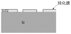
FIG. 3 is a schematic cross-sectional view of a base station for forming a silicon dioxide mask on a silicon substrate according to an embodiment of the present invention;
fig. 4 is a schematic cross-sectional structure diagram of a sample wafer after a passivation step S1 in the deep silicon etching method according to the embodiment of the present invention;
fig. 5 is a schematic cross-sectional structure diagram of the substrate after the etching step S2 in the deep silicon etching method according to the embodiment of the present invention;
fig. 6 is a schematic cross-sectional structure diagram of the substrate after the cleaning step S3 in the deep silicon etching method according to the embodiment of the present invention;
FIG. 7 is a scanning electron microscope image of a raised structure of a sample wafer using a conventional deep silicon etching process;
FIG. 8 is a scanning electron microscope image of a groove structure of a sample wafer using a conventional deep silicon etching process;
FIG. 9 is a scanning electron microscope image of a raised structure of a sample wafer according to an embodiment of the present invention;
FIG. 10 is a scanning electron microscope image of a groove structure of a sample wafer according to an embodiment of the present invention.
Detailed Description
The invention is described in further detail below with reference to the figures and the embodiments.
A Bosch process commonly used in deep silicon etching is shown in fig. 1. And alternately introducing etching gas SF6 and passivation gas C4F8 into the chamber, respectively carrying out etching and passivation steps, and repeatedly alternating the etching and the passivation to form a deep groove structure.
However, such Bosch process is prone to significant periodic scalloping on the trench sidewalls, which can be fatal defects for some devices. And the etching gas C4F8 is used as refractory fluorine-containing greenhouse gas, has higher greenhouse effect and is not beneficial to environmental protection. In addition, because the passivation film on the side wall is not removed in the alternating process of etching and passivation, the thickness of the passivation layer on the side wall close to the notch has a cumulative effect, which not only affects the performance of some devices (such as DRAM memories), but also is easy to have an etching stop effect for the process with the etching depth exceeding 200 microns and the CD value less than 0.13 micron. Fig. 7 and 8 are a scanning electron microscope image of a protruding structure of a sample wafer and a scanning electron microscope image of a groove structure section under a deep silicon etching process in a conventional process, respectively.
To avoid the above problems, the embodiment of the present invention performs the following three-step deep silicon etching process, as shown in fig. 2.
Most of the photoresist components are C-H compounds, which are easily oxidized and etched in the cleaning step S3 to reduce the etching selectivity, and the present embodiment uses Plasma Enhanced Chemical Vapor Deposition (PECVD) equipment to deposit 300nm SiO instead of using conventional organic colloid as mask layer2As hard mask layer, using 5350 photoresist to complete photoetching and patterning on the mask layer, and wet etching SiO with BOE etching solution2And forming a convex and concave structure on the surface of the silicon dioxide mask layer by using the mask layer, and removing the photoresist by using acetone as stripping liquid. SiO 22The hard mask fabrication flow is shown in figure 3.
S1, pre-etching the silicon wafer by using an etching machine containing ICP-RF double power supplies.
S2, pre-treating the substrate surface before the passivation step S1. Introducing 20sccm C4F6+80sccm O2And removing the native oxide layer on the surface of the silicon wafer. The step should control the pressure of the chamber to be adjusted to 20mtorr, and the surface structure of the mask layer is not damaged, and polymer deposition is not easy to generate.
The etching gas composition in the chamber is ensured to be correct after pre-aeration for 30s before the power is turned on, and then the ICP power supply 1300w is started to ensure that the gas is fully ionized, namely the RF power supply 100 w. The RF power should be adjusted to maintain the DC-Bias at 200V-400V depending on the substrate material to which the substrate is attached. In the embodiment, 317V DC-bias can be generated by using a 100W RF power supply, so that a larger physical etching effect is formed, and the native oxide layer on the surface of the silicon wafer is effectively removed.
100sccm C is introduced in the passivation step of S34F6And 5sccm SF6。
By C4F6Is a passivation gas due to the C of chain-like molecular structure4F6The compound is decomposed quickly to form passivation free radicals, and can be attached quickly to form a passivation film. Meanwhile, the film formed by the chain-shaped molecular structure is easier to be removed by chemical etching, which is beneficial to the cleaning step of S3, and in addition, C4F6Very low greenhouse effect, and C4F6Compared with etching gas, the volume fraction of perfluorinated compounds (PFCs) as greenhouse gases in the exhaust gas can be respectively reduced by 82%, and the method has good environmental friendliness.
A small amount of etching gas SF is introduced in the passivation step6The method is convenient for switching different steps, and simultaneously, the F/C ratio and the isotropic etching can be adjusted, thereby being beneficial to improving the etching steepness. The chamber pressure is adjusted to 40-80mtorr while the step is performed, which is higher than the pressure set in the pre-cleaning step, so that the (C-F)2 radicals can sufficiently react to form a passivation film.
Then starting ICP power supply 900 and 1100W to fully ionize C4F6Passivating gases benefiting from small amounts of SF6The ionization promoting effect. According to different structures of the carrier plate material and the etching sample device, the RF power supply is adjusted to 10-35W, in the embodiment, the aluminum sheet is used as the carrier plate, and the RF power supply 15W is adjusted to generate 48V DC-bias, so that C-F free radicals can be stably attached to the surface of the substrate to form a passivation film.
In addition, the substrate temperature is maintained at 5-40 ℃, and the evaporation effect of the product is not favorable for the adhesion of the passivation film due to the excessively high temperature. Due to C4F6The easy-to-break chain molecular structure can quickly generate a metastable film, so that the passivation time is only 3-5 s. Fig. 4 is a schematic cross-sectional structure diagram of the sample after the passivation step S1.
5sccm C is introduced in the etching step of S44F6And 100sccmsF6. Wherein SF6As an etching gas, F-containing plasma with extremely high concentration is generated after ionization, and high-efficiency chemical etching effect is provided. A small amount of passivation gas C is introduced in the etching step4F6Only the switching among different steps is convenient, and the F/C ratio and the isotropic etching can be adjusted, thereby being beneficial to slowing down the formation of the scallop-shaped structure.
When the step is carried out, the pressure of the chamber is required to be adjusted to be 40-80mtorr, the pressure in the step is set to be close to the pressure in the passivation step, so that the equipment can be conveniently adjusted in different steps, the gas is more easily ignited and ionized compared with the high-pressure cavity environment, high-density F-containing plasma is formed, and the etching rate and uniformity are improved.
After the pressure is adjusted, the etching gas can be fully ionized by starting the ICP power source 1100-1300W. According to different structures of a carrying disc material and an etched sample device, an RF power supply of 10-35W is adjusted, in the embodiment, an aluminum sheet is used as a carrying plate, 157V DC-bias can be generated by adjusting 30W of the RF power supply, the plasma in the cavity can move vertically to the surface of the sample, and the passive film on the vertical surface of the sample can be effectively removed without damaging the passive film on the side wall through directional physical impact. In addition, the temperature of the substrate is regulated to be 5-40 ℃, and the high temperature can cause rapid etching, so that the transverse etching is serious, and obvious scallop veins are formed. Since the etching step has a more pronounced thermal reaction formation, the back helium leak rate needs to be controlled, and the experiment uses 10Torr back helium and controls the leak rate to be less than 3 sccm. Since the metastable passivation film generated by C4F6 can be easily removed, the etching time is controlled to 6-8 s. Fig. 5 is a schematic cross-sectional structure diagram of the sample wafer after the etching step S2.
S5 purge step, introduce 80sccm O2And 10sccm Ar, wherein O2The main cleaning gas can be ionized to generate chemical reaction etching with the side wall passivation film, so that the side wall passivation film is stripped. Ar is used as an auxiliary gas to increase O2The ionization degree and the certain physical etching are provided, so that the residual etching products at the bottom of the deep groove can be bombarded, and the etching roughness is further optimized.
When the step S3 is carried out, the optimal cavity pressure is adjusted to be between 30 and 60mtorr according to the cavity environment of different equipment, the damage of a mask on the surface layer of a sample caused by the increase of physical etching is avoided, and the discharge of etching products and the removal of products at the bottom of a deep groove are facilitated.
After the pressure adjustment is finished, the ICP power supply is started at 800-1500W to ensure that O is2And fully ionizing, and simultaneously adjusting the RF power supply by 5-20W according to different structures of the carrying disc material and the etching sample device to enable the lower electrode to generate a small amount of self-bias voltage, so as to ensure that oxygen plasma is chemically etched in an infiltration mode.
S4, and circulating S1-S3 until the etching depth is reached, and finishing the etching.
In the embodiment, the aluminum sheet is used as the carrier plate, 16V DC-bias can be generated by adjusting the RF power supply 5W, the etching product at the bottom of the groove can be effectively removed, and excessive physical bombardment etching is avoided. According to the etching depth of the sample wafer and the environmental difference of the equipment cavity, the cleaning time can be controlled to be 5-30 s. Fig. 6 is a schematic cross-sectional view of the coupon after the cleaning step S3.
The invention improves the abnormal shapes of the scallop veins and the like by changing the types of gases in the passivation step and adding the cleaning step, effectively removes the accumulation of the side wall passivation film, prevents the peeling problem of the side wall passivation film, delays the etching termination effect and reduces the greenhouse effect. Fig. 9 and fig. 10 are scanning electron microscope images of a protruding structure and a groove structure of a sample wafer, respectively, provided by an embodiment of the present invention.
Therefore, the implementation of the invention overcomes the problems of side wall passive film stripping, fan-scallop texture and the like in the traditional deep silicon etching process.
Claims (8)
Priority Applications (1)
| Application Number | Priority Date | Filing Date | Title |
|---|---|---|---|
| CN202210254286.0A CN114664648A (en) | 2022-03-15 | 2022-03-15 | Silicon etching method |
Applications Claiming Priority (1)
| Application Number | Priority Date | Filing Date | Title |
|---|---|---|---|
| CN202210254286.0A CN114664648A (en) | 2022-03-15 | 2022-03-15 | Silicon etching method |
Publications (1)
| Publication Number | Publication Date |
|---|---|
| CN114664648A true CN114664648A (en) | 2022-06-24 |
Family
ID=82028989
Family Applications (1)
| Application Number | Title | Priority Date | Filing Date |
|---|---|---|---|
| CN202210254286.0A Pending CN114664648A (en) | 2022-03-15 | 2022-03-15 | Silicon etching method |
Country Status (1)
| Country | Link |
|---|---|
| CN (1) | CN114664648A (en) |
Cited By (1)
| Publication number | Priority date | Publication date | Assignee | Title |
|---|---|---|---|---|
| CN116177550A (en) * | 2023-03-09 | 2023-05-30 | 浙江大学 | Surface passivation method and application of a kind of silicon nanometer material |
Citations (14)
| Publication number | Priority date | Publication date | Assignee | Title |
|---|---|---|---|---|
| US20070000868A1 (en) * | 2005-06-29 | 2007-01-04 | Kabushiki Kaisha Toshiba | Dry etching method |
| US7166536B1 (en) * | 1999-04-29 | 2007-01-23 | Robert Bosch Gmbh | Methods for plasma etching of silicon |
| US20070030309A1 (en) * | 2005-08-08 | 2007-02-08 | Silverbrook Research Pty Ltd | Method suitable for etching hydrophillic trenches in a substrate |
| CN101290866A (en) * | 2006-12-13 | 2008-10-22 | 应用材料股份有限公司 | groove etching method |
| KR20090025518A (en) * | 2007-09-06 | 2009-03-11 | 주식회사 래디언테크 | Wafer Etching Method |
| CN102431960A (en) * | 2011-12-07 | 2012-05-02 | 华中科技大学 | Silicon through hole etching method |
| US20120270404A1 (en) * | 2011-04-25 | 2012-10-25 | Applied Materials, Inc | Methods for etching through-silicon vias with tunable profile angles |
| CN104347389A (en) * | 2013-07-23 | 2015-02-11 | 中微半导体设备(上海)有限公司 | Plasma etching method |
| CN104671193A (en) * | 2013-12-03 | 2015-06-03 | 北京北方微电子基地设备工艺研究中心有限责任公司 | Deep silicon etching method |
| CN105185704A (en) * | 2015-08-05 | 2015-12-23 | 成都嘉石科技有限公司 | Deep silicon etching method |
| CN105584986A (en) * | 2014-10-23 | 2016-05-18 | 中国科学院微电子研究所 | A silicon deep hole etching method |
| CN105600740A (en) * | 2015-12-23 | 2016-05-25 | 苏州工业园区纳米产业技术研究院有限公司 | Method for preparing high aspect ratio silicon microstructure on basis of deep reactive ion etching technology |
| CN110171802A (en) * | 2019-07-11 | 2019-08-27 | 江苏鲁汶仪器有限公司 | A kind of deep silicon etching method of MEMS |
| CN111243951A (en) * | 2020-01-22 | 2020-06-05 | 北京北方华创微电子装备有限公司 | Deep silicon etching method |
-
2022
- 2022-03-15 CN CN202210254286.0A patent/CN114664648A/en active Pending
Patent Citations (14)
| Publication number | Priority date | Publication date | Assignee | Title |
|---|---|---|---|---|
| US7166536B1 (en) * | 1999-04-29 | 2007-01-23 | Robert Bosch Gmbh | Methods for plasma etching of silicon |
| US20070000868A1 (en) * | 2005-06-29 | 2007-01-04 | Kabushiki Kaisha Toshiba | Dry etching method |
| US20070030309A1 (en) * | 2005-08-08 | 2007-02-08 | Silverbrook Research Pty Ltd | Method suitable for etching hydrophillic trenches in a substrate |
| CN101290866A (en) * | 2006-12-13 | 2008-10-22 | 应用材料股份有限公司 | groove etching method |
| KR20090025518A (en) * | 2007-09-06 | 2009-03-11 | 주식회사 래디언테크 | Wafer Etching Method |
| US20120270404A1 (en) * | 2011-04-25 | 2012-10-25 | Applied Materials, Inc | Methods for etching through-silicon vias with tunable profile angles |
| CN102431960A (en) * | 2011-12-07 | 2012-05-02 | 华中科技大学 | Silicon through hole etching method |
| CN104347389A (en) * | 2013-07-23 | 2015-02-11 | 中微半导体设备(上海)有限公司 | Plasma etching method |
| CN104671193A (en) * | 2013-12-03 | 2015-06-03 | 北京北方微电子基地设备工艺研究中心有限责任公司 | Deep silicon etching method |
| CN105584986A (en) * | 2014-10-23 | 2016-05-18 | 中国科学院微电子研究所 | A silicon deep hole etching method |
| CN105185704A (en) * | 2015-08-05 | 2015-12-23 | 成都嘉石科技有限公司 | Deep silicon etching method |
| CN105600740A (en) * | 2015-12-23 | 2016-05-25 | 苏州工业园区纳米产业技术研究院有限公司 | Method for preparing high aspect ratio silicon microstructure on basis of deep reactive ion etching technology |
| CN110171802A (en) * | 2019-07-11 | 2019-08-27 | 江苏鲁汶仪器有限公司 | A kind of deep silicon etching method of MEMS |
| CN111243951A (en) * | 2020-01-22 | 2020-06-05 | 北京北方华创微电子装备有限公司 | Deep silicon etching method |
Non-Patent Citations (1)
| Title |
|---|
| MOHAMED GAD-EL-HAK编: "《微机电系统设计与加工》", 28 February 2010, 机械工业出版社, pages: 6 - 8 * |
Cited By (2)
| Publication number | Priority date | Publication date | Assignee | Title |
|---|---|---|---|---|
| CN116177550A (en) * | 2023-03-09 | 2023-05-30 | 浙江大学 | Surface passivation method and application of a kind of silicon nanometer material |
| CN116177550B (en) * | 2023-03-09 | 2024-02-27 | 浙江大学 | A surface passivation method and use of silicon nanomaterials |
Similar Documents
| Publication | Publication Date | Title |
|---|---|---|
| US12154792B2 (en) | Plasma etching method | |
| US5384009A (en) | Plasma etching using xenon | |
| US20070026677A1 (en) | Method for plasma etching performance enhancement | |
| CN102800552B (en) | Substrate processing method using same | |
| KR100255405B1 (en) | Dry etching method | |
| CN101521158A (en) | Plasma etching method and plasma etching apparatus | |
| CN114783867A (en) | Silicon oxide etching method | |
| TW200847270A (en) | Plasma etching method, plasma etching device, control program and computer storage medium | |
| CN112997280A (en) | Dry etching method | |
| CN111627859A (en) | Semiconductor structure and forming method thereof | |
| CN114664648A (en) | Silicon etching method | |
| JP2009064991A (en) | High-k film dry etching method | |
| JP2687787B2 (en) | Dry etching method | |
| JP3094470B2 (en) | Dry etching method | |
| JPS6356312B2 (en) | ||
| TWI892472B (en) | Etching method using oxygen-containing hydrofluorocarbon | |
| CN101331092B (en) | Notch stop pulsing process for plasma processing system | |
| CN114664653B (en) | A silicon nitride etching method | |
| CN117253788A (en) | Sidewall etching method and semiconductor process equipment | |
| JP2022169464A (en) | Substrate processing method and substrate processing apparatus | |
| TWI892471B (en) | Etching method for forming a high aspect ratio aperture using oxygen-containing hydrofluorocarbon | |
| JP3079656B2 (en) | Dry etching method | |
| CN101052536A (en) | Methods of processing a substrate with minimal scalloping | |
| JP5154013B2 (en) | Dry etching method | |
| JPH053177A (en) | Dry etching method |
Legal Events
| Date | Code | Title | Description |
|---|---|---|---|
| PB01 | Publication | ||
| PB01 | Publication | ||
| SE01 | Entry into force of request for substantive examination | ||
| SE01 | Entry into force of request for substantive examination | ||
| RJ01 | Rejection of invention patent application after publication | ||
| RJ01 | Rejection of invention patent application after publication |
Application publication date: 20220624 |