CN114417759B - Design method of trigger unit - Google Patents
Design method of trigger unit Download PDFInfo
- Publication number
- CN114417759B CN114417759B CN202210107336.2A CN202210107336A CN114417759B CN 114417759 B CN114417759 B CN 114417759B CN 202210107336 A CN202210107336 A CN 202210107336A CN 114417759 B CN114417759 B CN 114417759B
- Authority
- CN
- China
- Prior art keywords
- clock
- signal
- edge
- trigger
- gating circuit
- Prior art date
- Legal status (The legal status is an assumption and is not a legal conclusion. Google has not performed a legal analysis and makes no representation as to the accuracy of the status listed.)
- Active
Links
Images





Classifications
-
- G—PHYSICS
- G06—COMPUTING OR CALCULATING; COUNTING
- G06F—ELECTRIC DIGITAL DATA PROCESSING
- G06F30/00—Computer-aided design [CAD]
- G06F30/30—Circuit design
- G06F30/32—Circuit design at the digital level
- G06F30/33—Design verification, e.g. functional simulation or model checking
-
- G—PHYSICS
- G06—COMPUTING OR CALCULATING; COUNTING
- G06F—ELECTRIC DIGITAL DATA PROCESSING
- G06F30/00—Computer-aided design [CAD]
- G06F30/30—Circuit design
- G06F30/32—Circuit design at the digital level
- G06F30/327—Logic synthesis; Behaviour synthesis, e.g. mapping logic, HDL to netlist, high-level language to RTL or netlist
-
- G—PHYSICS
- G06—COMPUTING OR CALCULATING; COUNTING
- G06F—ELECTRIC DIGITAL DATA PROCESSING
- G06F30/00—Computer-aided design [CAD]
- G06F30/30—Circuit design
- G06F30/32—Circuit design at the digital level
- G06F30/33—Design verification, e.g. functional simulation or model checking
- G06F30/3308—Design verification, e.g. functional simulation or model checking using simulation
- G06F30/3312—Timing analysis
-
- H—ELECTRICITY
- H03—ELECTRONIC CIRCUITRY
- H03K—PULSE TECHNIQUE
- H03K19/00—Logic circuits, i.e. having at least two inputs acting on one output; Inverting circuits
- H03K19/0008—Arrangements for reducing power consumption
- H03K19/0016—Arrangements for reducing power consumption by using a control or a clock signal, e.g. in order to apply power supply
-
- H—ELECTRICITY
- H03—ELECTRONIC CIRCUITRY
- H03K—PULSE TECHNIQUE
- H03K3/00—Circuits for generating electric pulses; Monostable, bistable or multistable circuits
- H03K3/02—Generators characterised by the type of circuit or by the means used for producing pulses
- H03K3/027—Generators characterised by the type of circuit or by the means used for producing pulses by the use of logic circuits, with internal or external positive feedback
- H03K3/037—Bistable circuits
-
- G—PHYSICS
- G06—COMPUTING OR CALCULATING; COUNTING
- G06F—ELECTRIC DIGITAL DATA PROCESSING
- G06F2117/00—Details relating to the type or aim of the circuit design
- G06F2117/04—Clock gating
-
- Y—GENERAL TAGGING OF NEW TECHNOLOGICAL DEVELOPMENTS; GENERAL TAGGING OF CROSS-SECTIONAL TECHNOLOGIES SPANNING OVER SEVERAL SECTIONS OF THE IPC; TECHNICAL SUBJECTS COVERED BY FORMER USPC CROSS-REFERENCE ART COLLECTIONS [XRACs] AND DIGESTS
- Y02—TECHNOLOGIES OR APPLICATIONS FOR MITIGATION OR ADAPTATION AGAINST CLIMATE CHANGE
- Y02D—CLIMATE CHANGE MITIGATION TECHNOLOGIES IN INFORMATION AND COMMUNICATION TECHNOLOGIES [ICT], I.E. INFORMATION AND COMMUNICATION TECHNOLOGIES AIMING AT THE REDUCTION OF THEIR OWN ENERGY USE
- Y02D10/00—Energy efficient computing, e.g. low power processors, power management or thermal management
Landscapes
- Engineering & Computer Science (AREA)
- Computer Hardware Design (AREA)
- Physics & Mathematics (AREA)
- Theoretical Computer Science (AREA)
- General Engineering & Computer Science (AREA)
- Evolutionary Computation (AREA)
- Geometry (AREA)
- General Physics & Mathematics (AREA)
- Computing Systems (AREA)
- Mathematical Physics (AREA)
- Manipulation Of Pulses (AREA)
- Logic Circuits (AREA)
Abstract
本申请公开了触发单元的设计方法。该设计方法包括:在数字电路中分析时钟控制信号的信号延迟;根据时钟控制信号的信号延迟,在多个不同类型的时钟门控电路中选择时钟门控电路;以及将至少一个边沿触发器和选择的时钟门控电路组合成触发单元,其中,多个不同类型的时钟门控电路根据时钟控制信号启用或屏蔽第一时钟信号以产生第二时钟信号,边沿触发器在第二时钟信号的边沿传输数据。该触发单元的设计方法根据时钟控制信号的延迟条件,从多个不同类型的时钟门控电路选择时钟门控电路,不仅可以消除时钟门控电路产生的时钟信号的毛刺,而且可以减少时钟门控电路的逻辑元件数量和降低时钟门控电路的功耗,适用于任意数量边沿触发器的触发器组。

The application discloses a design method of a trigger unit. The design method includes: analyzing the signal delay of a clock control signal in a digital circuit; selecting a clock gating circuit from a plurality of different types of clock gating circuits according to the signal delay of the clock control signal; and combining at least one edge trigger and Selected clock gating circuits are combined into a trigger unit, wherein a plurality of different types of clock gating circuits enable or disable the first clock signal to generate a second clock signal according to the clock control signal, and the edge trigger operates on the edge of the second clock signal transfer data. The design method of the trigger unit selects the clock gating circuit from multiple different types of clock gating circuits according to the delay condition of the clock control signal, which can not only eliminate the glitch of the clock signal generated by the clock gating circuit, but also reduce the clock gating The number of logic elements of the circuit and the reduction of power consumption of the clock gating circuit are suitable for flip-flop groups with any number of edge flip-flops.
Description
技术领域technical field
本发明涉及集成电路技术,更具体地,涉及触发单元的设计方法。The present invention relates to integrated circuit technology, and more specifically, to a design method of a trigger unit.
背景技术Background technique
电子设计自动化软件(EDA)是集成电路的功能设计、综合、验证、物理设计等流程的重要工具。在数字电路设计EDA中,标准单元库是集成电路芯片后端设计过程中的基础部分。采用预先设计好的优化的库单元进行自动逻辑综合和版图布局布线,可以提高设计效率。经过优化的库单元可以提高电路性能和降低功耗。Electronic design automation software (EDA) is an important tool for the functional design, synthesis, verification, physical design and other processes of integrated circuits. In the digital circuit design EDA, the standard cell library is the basic part in the back-end design process of the integrated circuit chip. Using pre-designed optimized library cells for automatic logic synthesis and layout placement and routing can improve design efficiency. Optimized library cells can improve circuit performance and reduce power consumption.
在集成电路的数字部分中,采用门电路将多个信号经过组合逻辑产生逻辑运算结果,采用边沿触发器存储逻辑运算结果。按照逻辑运算的不同,门电路可以分为与门、或门、非门、与非门、或门、与或门、异或门等。门电路的逻辑运算结果例如是脉冲信号,基于脉冲信号产生与逻辑状态相对应的稳态电平信号。In the digital part of the integrated circuit, gate circuits are used to pass multiple signals through combinational logic to generate logic operation results, and edge triggers are used to store the logic operation results. According to different logic operations, gate circuits can be divided into AND gates, OR gates, NOT gates, NAND gates, OR gates, AND-OR gates, XOR gates, etc. The logic operation result of the gate circuit is, for example, a pulse signal, and a steady-state level signal corresponding to a logic state is generated based on the pulse signal.
边沿触发器是具有记忆功能的信息存储器件,用于存储记忆逻辑运算结果。例如,边沿触发器是构成多种时序数字电路模块中的最基本逻辑单元,在数字电路模块中是一种重要的单元电路。参见图1和图2,根据边沿触发器的类型,边沿触发器110在时钟信号的上升沿或下降沿触发,允许输入数据从输入端传输到输出端以获得输出数据。边沿触发器110例如是D型触发器。例如,D型触发器在时钟信号的触发边沿传输数据,在下一次触发边沿前维持数据不变。The edge trigger is an information storage device with memory function, which is used to store the result of memory logic operation. For example, the edge trigger is the most basic logic unit in various sequential digital circuit modules, and is an important unit circuit in digital circuit modules. Referring to FIGS. 1 and 2 , depending on the type of edge trigger, the
边沿触发器的功耗包括静态功耗和动态功耗,其中,静态功耗主要由泄漏电流引起,动态功耗主要由信号翻转功耗引起。边沿触发器的数据信号翻转导致后级组合逻辑产生附加的数据功耗,时钟信号的翻转也会产生边沿触发器自身的时钟功耗。The power consumption of the edge trigger includes static power consumption and dynamic power consumption. Among them, the static power consumption is mainly caused by the leakage current, and the dynamic power consumption is mainly caused by the signal inversion power consumption. The inversion of the data signal of the edge trigger will cause additional data power consumption in the combinational logic of the subsequent stage, and the inversion of the clock signal will also generate the clock power consumption of the edge trigger itself.
因此,期望对数字电路EDA标准单元库中的边沿触发器进行优化设计,进一步降低边沿触发器的动态功耗。Therefore, it is expected to optimize the design of the edge trigger in the digital circuit EDA standard cell library to further reduce the dynamic power consumption of the edge trigger.
发明内容Contents of the invention
鉴于上述问题,本发明的目的在于提供触发单元的设计方法,根据时钟控制信号的延迟条件,从多个不同类型的时钟门控电路选择时钟门控电路,以减少时钟门控电路的逻辑元件数量和降低时钟门控电路的功耗。In view of the problems referred to above, the object of the present invention is to provide a design method of trigger unit, according to the delay condition of the clock control signal, select the clock gating circuit from a plurality of different types of clock gating circuits, to reduce the number of logic elements of the clock gating circuit and reduce the power consumption of the clock gating circuit.
根据本发明,提供一种触发单元的设计方法,包括:在数字电路中分析时钟控制信号的信号延迟;根据时钟控制信号的信号延迟,在多个不同类型的时钟门控电路中选择时钟门控电路;以及将至少一个边沿触发器和所述选择的时钟门控电路组合成触发单元,其中,所述多个不同类型的时钟门控电路根据所述时钟控制信号启用或屏蔽第一时钟信号以产生第二时钟信号,所述边沿触发器在所述第二时钟信号的边沿传输数据。According to the present invention, a design method of a trigger unit is provided, including: analyzing the signal delay of the clock control signal in a digital circuit; circuit; and at least one edge trigger and the selected clock gating circuit are combined into a trigger unit, wherein the plurality of different types of clock gating circuits enable or shield the first clock signal according to the clock control signal to A second clock signal is generated, and the edge trigger transmits data at an edge of the second clock signal.
优选地,所述多个不同类型的时钟门控电路包括第一时钟门控电路和第二时钟门控电路中的至少一种,所述第一时钟门控电路和所述第二时钟门控电路至少在所述时钟控制信号从有效状态翻转至无效状态的时钟周期中,将所述第二时钟信号维持为预定电平。Preferably, the multiple different types of clock gating circuits include at least one of a first clock gating circuit and a second clock gating circuit, and the first clock gating circuit and the second clock gating The circuit maintains the second clock signal at a predetermined level at least during a clock period in which the clock control signal toggles from an active state to an inactive state.
优选地,在所述时钟控制信号维持无效状态的时钟周期中,所述第一时钟门控电路和所述第二时钟门控电路将所述第二时钟信号维持为所述预定电平。Preferably, the first clock gating circuit and the second clock gating circuit maintain the second clock signal at the predetermined level during a clock cycle in which the clock control signal remains inactive.
优选地,在所述时钟控制信号从无效状态翻转为有效状态的时钟周期中,所述第一时钟门控电路和所述第二时钟门控电路复制所述第一时钟信号作为所述第二时钟信号。Preferably, in a clock cycle in which the clock control signal toggles from an inactive state to an active state, the first clock gating circuit and the second clock gating circuit replicate the first clock signal as the second clock signal.
优选地,在所述时钟控制信号维持有效状态的时钟周期中,所述第一时钟门控电路和所述第二时钟门控电路复制所述第一时钟信号作为所述第二时钟信号。Preferably, the first clock gating circuit and the second clock gating circuit replicate the first clock signal as the second clock signal during a clock period in which the clock control signal maintains an active state.
优选地,所述第一时钟门控电路对所述时钟控制信号的反相信号和所述第一时钟信号进行逻辑或运算以产生所述第二时钟信号。Preferably, the first clock gating circuit performs a logical OR operation on the inversion signal of the clock control signal and the first clock signal to generate the second clock signal.
优选地,所述第二时钟门控电路对所述时钟控制信号和所述第一时钟信号进行逻辑与运算以产生所述第二时钟信号。Preferably, the second clock gating circuit performs a logical AND operation on the clock control signal and the first clock signal to generate the second clock signal.
优选地,所述多个不同类型的时钟门控电路还包括第三时钟门控电路,所述第三时钟门控电路至少在所述时钟控制信号从有效状态翻转至无效状态的下一个时钟周期中,将所述第二时钟信号维持为预定电平。Preferably, the multiple different types of clock gating circuits further include a third clock gating circuit, the third clock gating circuit at least in the next clock cycle when the clock control signal is turned from an active state to an inactive state , maintaining the second clock signal at a predetermined level.
优选地,所述第三时钟门控电路对所述时钟控制信号的锁存信号和所述第一时钟信号进行逻辑与运算以产生所述第二时钟信号。Preferably, the third clock gating circuit performs a logical AND operation on the latch signal of the clock control signal and the first clock signal to generate the second clock signal.
优选地,所述时钟控制信号的信号延迟在最小延迟和最大延迟之间的范围内变化。Preferably, the signal delay of said clock control signal varies within a range between a minimum delay and a maximum delay.
优选地,在所述最小延迟和所述最大延迟均位于所述第一时钟信号信号的第一电平阶段的情形下,根据所述第一电平阶段的开始边沿选择所述第一时钟门控电路和所述第二时钟门控电路之一。Preferably, in the case that both the minimum delay and the maximum delay are located in the first level phase of the first clock signal, the first clock gate is selected according to the start edge of the first level phase control circuit and one of the second clock gating circuit.
优选地,在所述第一电平阶段的开始边沿为上升沿的情形下,所述选择的时钟门控电路为所述第一时钟门控电路。Preferably, when the start edge of the first level phase is a rising edge, the selected clock gating circuit is the first clock gating circuit.
优选地,在所述第一电平阶段的开始边沿为下降沿的情形下,所述选择的时钟门控电路为所述第二时钟门控电路。Preferably, when the start edge of the first level phase is a falling edge, the selected clock gating circuit is the second clock gating circuit.
优选地,所述预定电平为所述第一电平阶段的电平。Preferably, the predetermined level is the level of the first level stage.
优选地,在所述最小延迟和所述最大延迟分别位于所述第一时钟信号的第一电平阶段和第二电平阶段的情形下,所述选择的时钟门控电路为第三时钟门控电路。Preferably, in the case that the minimum delay and the maximum delay are respectively located in the first level stage and the second level stage of the first clock signal, the selected clock gating circuit is a third clock gate control circuit.
优选地,所述预定电平为所述第二电平阶段的电平。Preferably, the predetermined level is the level of the second level stage.
优选地,组合成触发单元的步骤包括:根据选择的时钟门控电路的类型和所述边沿触发器的类型,选择所述边沿触发器传输数据的时钟周期。Preferably, the step of combining into a trigger unit includes: selecting a clock period for the edge trigger to transmit data according to the type of the selected clock gating circuit and the type of the edge trigger.
优选地,在所述第一电平阶段的开始边沿与所述边沿触发器的触发边沿相同的情形下,在所述时钟控制信号翻转的时钟周期,所述第二时钟信号提供所述边沿触发器的触发边沿。Preferably, in the case where the start edge of the first level stage is the same as the trigger edge of the edge trigger, the second clock signal provides the edge trigger trigger edge of the device.
优选地,在所述第一电平阶段的开始边沿与所述边沿触发器的触发边沿相反的情形下,在所述时钟控制信号翻转的时钟周期的前一时钟周期,所述第二时钟信号提供所述边沿触发器的触发边沿。Preferably, in the case where the start edge of the first level phase is opposite to the trigger edge of the edge trigger, the second clock signal A trigger edge of the edge trigger is provided.
优选地,组合成触发单元的步骤包括:对所述第二时钟信号进行反相以产生第三时钟信号。Preferably, the step of combining into a trigger unit includes: inverting the second clock signal to generate a third clock signal.
优选地,在所述第一电平阶段的开始边沿与所述边沿触发器的触发边沿相同的情形下,在所述时钟控制信号翻转的时钟周期,所述第二时钟信号提供所述边沿触发器的触发边沿。Preferably, in the case where the start edge of the first level stage is the same as the trigger edge of the edge trigger, the second clock signal provides the edge trigger trigger edge of the device.
优选地,在所述第一电平阶段的开始边沿与所述边沿触发器的触发边沿相反的情形下,在所述时钟控制信号翻转的时钟周期,所述第三时钟信号提供所述边沿触发器的触发边沿。Preferably, in the case where the start edge of the first level stage is opposite to the trigger edge of the edge trigger, the third clock signal provides the edge trigger trigger edge of the device.
优选地,所述时钟控制信号高电平表示有效状态,低电平表示无效状态。Preferably, a high level of the clock control signal indicates an active state, and a low level indicates an invalid state.
根据本发明的实施例,在触发单元的设计方法中,根据时钟控制信号的延迟条件,从多个不同类型的时钟门控电路选择时钟门控电路。利用不同类型的时钟门控电路在时钟控制信号的不同延迟条件下的电路特性,可以消除时钟门控电路产生的时钟信号的毛刺。在时钟控制信号维持无效状态的时钟周期中,时钟门控电路产生的第二时钟信号禁用边沿触发器的时钟翻转和数据传输,因而可以降低边沿触发器的动态功耗。According to an embodiment of the present invention, in the design method of the trigger unit, the clock gating circuit is selected from a plurality of different types of clock gating circuits according to the delay condition of the clock control signal. Utilizing the circuit characteristics of different types of clock gating circuits under different delay conditions of the clock control signal, the burr of the clock signal generated by the clock gating circuit can be eliminated. During the clock period when the clock control signal remains inactive, the second clock signal generated by the clock gating circuit disables clock inversion and data transmission of the edge trigger, thereby reducing dynamic power consumption of the edge trigger.
在优选的实施例中,在时钟控制信号的最小延迟和最大延迟的范围均位于单个电平阶段且该电平阶段的开始边沿为上升沿的情形下,选择第一时钟门控电路,所述第一时钟门控电路对所述时钟控制信号的反相信号和所述第一时钟信号进行逻辑或运算以产生所述第二时钟信号。可以消除时钟门控电路产生的时钟信号的毛刺。在时钟控制信号从有效状态翻转为无效状态的时钟周期中,时钟门控电路产生的第二时钟信号禁用边沿触发器的时钟翻转,因而可以降低边沿触发器的动态功耗。In a preferred embodiment, when the ranges of the minimum delay and the maximum delay of the clock control signal are both in a single level stage and the start edge of the level stage is a rising edge, the first clock gating circuit is selected, the The first clock gating circuit performs a logical OR operation on the inversion signal of the clock control signal and the first clock signal to generate the second clock signal. The glitch of the clock signal generated by the clock gating circuit can be eliminated. In the clock cycle when the clock control signal is turned from an active state to an inactive state, the second clock signal generated by the clock gating circuit disables clock inversion of the edge trigger, thereby reducing dynamic power consumption of the edge trigger.
在优选的实施例中,在时钟控制信号的最小延迟和最大延迟的范围均位于单个电平阶段且该电平阶段的开始边沿为下降沿的情形下,选择第二时钟门控电路,所述第二时钟门控电路对所述时钟控制信号和所述第一时钟信号进行逻辑与运算以产生所述第二时钟信号。可以消除时钟门控电路产生的时钟信号的毛刺。在时钟控制信号从有效状态翻转为无效状态的时钟周期中,时钟门控电路产生的第二时钟信号禁用边沿触发器的时钟翻转,因而可以降低边沿触发器的动态功耗。In a preferred embodiment, when the ranges of the minimum delay and the maximum delay of the clock control signal are both located in a single level stage and the start edge of the level stage is a falling edge, the second clock gating circuit is selected, the The second clock gating circuit performs a logical AND operation on the clock control signal and the first clock signal to generate the second clock signal. The glitch of the clock signal generated by the clock gating circuit can be eliminated. In the clock cycle when the clock control signal is turned from an active state to an inactive state, the second clock signal generated by the clock gating circuit disables clock inversion of the edge trigger, thereby reducing dynamic power consumption of the edge trigger.
在优选的实施例中,在选择第一时钟门控电路和第二时钟门控电路的情形下,即使省去锁存器,也可以消除时钟门控电路产生的时钟信号的毛刺。因而,时钟门控电路中使用的硬件逻辑较少,时钟门控电路自身的工作功耗较低。触发单元中的任意数量的边沿触发器可以组成共用时钟门控电路的触发器组。对于触发器组包含任意数量的边沿触发器的情形,例如,一个,两个,或多个,因时钟门控电路本身的功耗而增加的功耗远小于边沿触发器因时钟门控而减少的功耗,因此,触发单元始终可以实现功耗降低。In a preferred embodiment, when the first clock gating circuit and the second clock gating circuit are selected, even if the latch is omitted, the glitch of the clock signal generated by the clock gating circuit can be eliminated. Therefore, less hardware logic is used in the clock gating circuit, and the working power consumption of the clock gating circuit itself is lower. Any number of edge flip-flops in the flip-flop unit can form a flip-flop group that shares a clock gating circuit. For flip-flop groups containing any number of edge flip-flops, e.g., one, two, or more, the increase in power consumption due to the power consumption of the clock gating circuit itself is much less than the decrease in power consumption due to clock gating for the edge flip-flops power consumption, therefore, the trigger unit always achieves reduced power consumption.
进一步地,该触发单元的电路设计方法优化时钟门控电路和边沿触发器的组合,因而可以简化且版图布局面积减小,将时钟门控电路和边沿触发器的组合电路作为标准单元库的库单元,在不同的条件下应用以提高数字电路的性能和设计效率。Further, the circuit design method of the trigger unit optimizes the combination of the clock gating circuit and the edge trigger, so it can be simplified and the layout area is reduced, and the combined circuit of the clock gating circuit and the edge trigger is used as the library of the standard cell library unit, applied under different conditions to improve the performance and design efficiency of digital circuits.
附图说明Description of drawings
通过以下参照附图对本发明实施例的描述,本发明的上述以及其他目的、特征和优点将更为清楚。The above and other objects, features and advantages of the present invention will be more apparent through the following description of the embodiments of the present invention with reference to the accompanying drawings.
图1和图2分别示出集成电路中的边沿触发器的示意性电路图和波形图。1 and 2 respectively show a schematic circuit diagram and a waveform diagram of an edge trigger in an integrated circuit.
图3示出触发单元的示意性电路图。FIG. 3 shows a schematic circuit diagram of a trigger unit.
图4和图5分别示出根据现有技术的时钟门控电路的示意性电路图和波形图。4 and 5 respectively show a schematic circuit diagram and a waveform diagram of a clock gating circuit according to the prior art.
图6和图7a、图7b分别示出根据本发明第一实施例的时钟门控电路的示意性电路图和波形图。Fig. 6 and Fig. 7a and Fig. 7b respectively show a schematic circuit diagram and a waveform diagram of a clock gating circuit according to the first embodiment of the present invention.
图8和9a、图9b分别示出根据本发明第二实施例的时钟门控电路的示意性电路图和波形图。Figures 8 and 9a and Figure 9b respectively show a schematic circuit diagram and a waveform diagram of a clock gating circuit according to the second embodiment of the present invention.
图10示出根据本发明第三实施例的触发单元设计方法的流程图。FIG. 10 shows a flowchart of a trigger unit design method according to a third embodiment of the present invention.
图11示出在图10所示的触发单元设计方法中时钟门控电路和边沿触发器的一种组合方法。FIG. 11 shows a combination method of a clock gating circuit and an edge trigger in the trigger unit design method shown in FIG. 10 .
图12示出在图10所示的触发单元设计方法中时钟门控电路和边沿触发器的另一种组合方法。FIG. 12 shows another combination method of the clock gating circuit and the edge trigger in the trigger unit design method shown in FIG. 10 .
具体实施方式detailed description
以下将参照附图更详细地描述本发明。在各个附图中,相同的元件采用类似的附图标记来表示。为了清楚起见,附图中的各个部分没有按比例绘制。此外,可能未示出某些公知的部分。Hereinafter, the present invention will be described in more detail with reference to the accompanying drawings. In the various figures, identical elements are indicated with similar reference numerals. For the sake of clarity, various parts in the drawings have not been drawn to scale. Also, some well-known parts may not be shown.
在下文中描述了本发明的许多特定的细节,例如器件的结构、材料、尺寸、处理工艺和技术,以便更清楚地理解本发明。但正如本领域的技术人员能够理解的那样,可以不按照这些特定的细节来实现本发明。In the following, many specific details of the present invention are described, such as device structures, materials, dimensions, processing techniques and techniques, for a clearer understanding of the present invention. However, the invention may be practiced without these specific details, as will be understood by those skilled in the art.
本发明可以各种形式呈现,以下将描述其中一些示例。The invention can be embodied in various forms, some examples of which are described below.
图3示出触发单元的示意性电路图。触发单元200包括边沿触发器110和时钟门控电路130。时钟门控电路130用于边沿触发器110的时钟信号CK的门控。在本实施例中,边沿触发器110例如为D型触发器。FIG. 3 shows a schematic circuit diagram of a trigger unit. The
边沿触发器110包括数据输入端、数据输出端和时钟输入端。时钟门控电路130包括输入端、输出端和控制端。时钟门控电路130的输入端接收时钟信号CLK,输出端提供时钟信号CK,控制端接收时钟控制信号EN。边沿触发器110的数据输入端接收输入数据Di,时钟输入端接收时钟信号CK,数据输出端提供输出数据Do。The edge flip-
在时钟信号CK的触发边沿,例如上升沿,边沿触发器110将输入数据从数据输入端传送至数据输出端。因而,边沿触发器110的数据输出端的输出数据相对应的信号电平取决于时钟信号CK的触发边沿到来之前数据输入端的输入数据的信号电平,并且在时钟信号CK的触发边沿之后的一个时钟周期中维持不变。边沿触发器110的数据输出端可以包括两个互补输出端。On a trigger edge, such as a rising edge, of the clock signal CK, the edge flip-
时钟门控电路130对时钟控制信号EN和时钟信号CLK进行逻辑运算以产生边沿触发器110的时钟信号CK。The
在上述的触发单元中,时钟门控电路130根据时钟控制信号EN的状态控制时钟信号的传输。In the above trigger unit, the
在时钟控制信号EN维持有效的时钟周期中,时钟门控电路130将时钟信号CLK复制为时钟信号CK,时钟信号CK提供至边沿触发器110的时钟输入端,在时钟控制信号EN维持无效的时钟周期中,时钟门控电路130屏蔽时钟信号CLK,以及将时钟信号CK维持为预定电平。In the clock period when the clock control signal EN is maintained valid, the
在时钟信号CK维持为预定电平的情形下,时钟信号CK不能提供边沿触发器110的触发边沿,因此可以禁用边沿触发器110的时钟翻转和数据传输。进一步地,边沿触发器110阻止数据进入后级数字电路中,因而可以避免后级组合逻辑的数据信号翻转产生附加的数据功耗。In the case where the clock signal CK is maintained at a predetermined level, the clock signal CK cannot provide a trigger edge of the
图4示出根据现有技术的时钟门控电路的示意性电路图。参见图3,时钟门控电路130和边沿触发器110共同组成触发单元,时钟门控电路130向边沿触发器110提供时钟信号CK。Fig. 4 shows a schematic circuit diagram of a clock gating circuit according to the prior art. Referring to FIG. 3 , the
时钟门控电路130包括锁存器131和与门132。锁存器131在时钟信号CLK的第一电平阶段T1对时钟控制信号EN进行锁存,在时钟信号CLK的第二电平阶段T2传输时钟控制信号EN,与门对锁存信号EN_a和时钟信号CLK进行逻辑与运算以产生时钟信号CK。The
锁存器131包括第一输入端、第二输入端和输出端。与门132包括第一输入端、第二输入端和输出端。锁存器131的第一输入端接收时钟信号CLK,第二输入端接收时钟控制信号EN。与门132的第一输入端接收时钟信号CLK,第二输入端与锁存器131的输出端相连接,输出端提供时钟信号CK。The
以上升沿触发的边沿触发器为例,时钟控制信号EN以高电平表示有效状态、低电平表示无效状态为例进行说明。时钟信号CLK的每个时钟周期包括相邻上升沿之间的连续的第一电平阶段T1和第二电平阶段T2,第一电平阶段T1和第二电平阶段T2分别具有高电平和低电平。时钟信号CK提供边沿触发器110的触发边沿,边沿触发器110在触发边沿将输入数据从输入端传送至输出端。Taking an edge trigger triggered by a rising edge as an example, the clock control signal EN is described as an example where a high level indicates an active state and a low level indicates an invalid state. Each clock cycle of the clock signal CLK includes continuous first level phase T1 and second level phase T2 between adjacent rising edges, and the first level phase T1 and the second level phase T2 respectively have a high level and low level. The clock signal CK provides the triggering edge of the
参见图5,输入数据Di和时钟控制信号EN各自存在着相对于时钟信号边沿的信号延迟Td。信号延迟Td的最小延迟Tdmin和最大延迟Tdmax之间的区域分别采用阴影部分表示。时钟控制信号EN的信号延迟Td在最小延迟Tdmin和最大延迟Tdmax之间变化。Referring to FIG. 5 , the input data Di and the clock control signal EN each have a signal delay Td relative to the edge of the clock signal. Areas between the minimum delay Tdmin and the maximum delay Tdmax of the signal delay Td are indicated by hatching, respectively. The signal delay Td of the clock control signal EN varies between a minimum delay Tdmin and a maximum delay Tdmax.
如图5所示,最小延迟Tdmin和最大延迟Tdmax分别位于第一电平阶段T1和第二电平阶段T2中,时钟控制信号EN的翻转动作既可能发生在时钟信号CLK的第一电平阶段T1,也可能发生在时钟信号CLK的第二电平阶段T2。As shown in Figure 5, the minimum delay Tdmin and the maximum delay Tdmax are respectively located in the first level stage T1 and the second level stage T2, and the inversion of the clock control signal EN may occur in the first level stage of the clock signal CLK T1 may also occur in the second level phase T2 of the clock signal CLK.
在时刻t0,时钟信号CLK到达第一个上升沿,时钟控制信号EN有效。在时刻t0开始的一个时钟周期中,时钟控制信号EN从有效状态翻转为无效状态。在时钟信号CLK的第一电平阶段T1,锁存器131的输出端的锁存信号EN_a信号电平保持为前一状态,即,高电平。在时钟信号CLK的第二电平阶段T2,锁存器131将时钟控制信号EN从输入端传送至输出端。At time t0, the clock signal CLK reaches the first rising edge, and the clock control signal EN is valid. In a clock cycle starting from time t0, the clock control signal EN turns from an active state to an inactive state. In the first level phase T1 of the clock signal CLK, the signal level of the latch signal EN_a at the output terminal of the
如果时钟控制信号EN的信号延迟Td小于等于时钟信号CLK的第一电平阶段T1,则在时钟控制信号翻转的时钟周期中,锁存信号EN_a是时钟信号CLK的复制版本。如果时钟控制信号EN的信号延迟Td大于时钟信号CLK的第一电平阶段T1,则在时钟信号CLK的第二电平阶段T2,锁存信号EN_a中出现毛刺。时钟信号CK是时钟信号CLK和锁存信号EN_a的逻辑与运算结果,该逻辑与运算可以消除锁存信号EN_a在时钟信号CLK第二电平阶段T2的毛刺。If the signal delay Td of the clock control signal EN is less than or equal to the first level phase T1 of the clock signal CLK, the latch signal EN_a is a replica of the clock signal CLK in the clock period when the clock control signal is inverted. If the signal delay Td of the clock control signal EN is greater than the first level phase T1 of the clock signal CLK, a glitch occurs in the latch signal EN_a during the second level phase T2 of the clock signal CLK. The clock signal CK is a logical AND operation result of the clock signal CLK and the latch signal EN_a, and the logical AND operation can eliminate the glitch of the latch signal EN_a in the second level phase T2 of the clock signal CLK.
因此,在时刻t0开始的一个时钟周期中,时钟门控电路130将时钟信号CLK复制为时钟信号CK且提供时钟信号CK的上升沿,边沿触发器110的输出数据Do的信号电平与时刻t0的输入数据Di的信号电平一致,例如图5所示的低电平。Therefore, in a clock cycle starting from time t0, the
在时刻t1,时钟信号CLK到达第二个上升沿,时钟控制信号EN无效。在时刻t1开始的一个时钟周期中,时钟控制信号EN维持无效状态。在时钟信号CLK的第一电平阶段T1,锁存器131的输出端的锁存信号EN_a信号电平保持为前一状态,即,低电平。在时钟信号CLK的第二电平阶段T2,锁存器131将时钟控制信号EN从输入端传送至输出端。在这个时钟周期内,时钟控制信号EN维持低电平状态,因此EN_a也保持低电平,时钟信号CK经时钟信号CLK和锁存信号EN_a的与运算,结果也保持低电平。At time t1, the clock signal CLK reaches the second rising edge, and the clock control signal EN becomes invalid. During a clock cycle starting from time t1, the clock control signal EN remains inactive. During the first level phase T1 of the clock signal CLK, the signal level of the latch signal EN_a at the output terminal of the
在时刻t2,时钟信号CLK到达第三个上升沿,时钟控制信号EN无效。在时刻t2开始的一个时钟周期中,时钟控制信号EN从无效状态翻转为有效状态。在时钟信号CLK的第一电平阶段T1,锁存器131的输出端的锁存信号EN_a信号电平保持为前一状态,即,低电平。在时钟信号CLK的第二电平阶段T2,锁存器131将时钟控制信号EN从输入端传送至输出端。如果时钟控制信号EN的信号延迟Td小于等于时钟信号CLK的第一电平阶段T1,则在时钟控制信号翻转的时钟周期中,锁存信号EN_a是时钟信号CLK的复制版本。如果时钟控制信号EN的信号延迟Td大于时钟信号CLK的第一电平阶段T1,则在时钟信号CLK的第二电平阶段T2,锁存信号EN_a中出现毛刺。时钟信号CK是时钟信号CLK和锁存信号EN_a的逻辑与运算结果,该逻辑与运算可以消除锁存信号EN_a在时钟信号CLK第二电平阶段T2的毛刺。At time t2, the clock signal CLK reaches the third rising edge, and the clock control signal EN becomes invalid. In a clock cycle starting from time t2, the clock control signal EN is switched from an inactive state to an active state. During the first level phase T1 of the clock signal CLK, the signal level of the latch signal EN_a at the output terminal of the
因此,在时刻t1开始的两个时钟周期中,时钟门控电路130屏蔽时钟信号CLK且未提供时钟信号CK的上升沿,边沿触发器110的输出数据Do的信号电平与上一时钟周期的信号电平一致,例如图5所示的低电平。Therefore, in the two clock cycles starting from time t1, the
上述的时钟门控电路130根据时钟控制信号EN的状态控制时钟信号的传输。The aforementioned
在时钟控制信号EN从有效状态翻转至无效状态的时钟周期中,时钟门控电路130将时钟信号CLK复制为时钟信号CK。此时,时钟信号CK提供边沿触发器110的触发边沿,时钟门控电路130允许边沿触发器110的时钟翻转和数据传输,边沿触发器110提供的输出数据Do为当前触发边沿的输入数据Di。During the clock period when the clock control signal EN is switched from an active state to an inactive state, the
在时钟控制信号EN从无效状态翻转至有效状态的时钟周期中,时钟门控电路130屏蔽时钟信号CLK,以及将时钟信号CK维持为预定电平。此时,时钟信号CK未能提供边沿触发器110的触发边沿,时钟门控电路130禁用边沿触发器110的时钟翻转和数据传输,边沿触发器110维持前一触发边沿的输入数据Di,因而可以降低边沿触发器110的动态功耗。During the clock period when the clock control signal EN is switched from an inactive state to an active state, the
上述的时钟门控电路130对时钟控制信号EN的时序要求不高。如果希望在预定时刻禁用数据传输,则可以在预定时刻之前的最后一个整时钟周期中完成时钟控制信号EN从有效状态至无效状态的翻转动作,在预定时刻开始的最后一个时钟周期中完成时钟控制信号EN从无效状态至有效状态的翻转动作。The aforementioned
本发明人注意到,在数字电路EDA的标准单元库中提供的触发单元使用上述的时钟门控电路130。时钟门控电路130包括锁存器131,用于消除边沿触发器110的时钟信号CK中可能出现的毛刺。The inventor noticed that the trigger unit provided in the standard cell library of the digital circuit EDA uses the above-mentioned
然而,在锁存器131中使用的硬件逻辑较多,导致时钟门控电路130自身的工作功耗过高。时钟门控电路130自身的工作功耗甚至有可能超过边沿触发器因时钟门控而减少的功耗。在触发单元中,时钟门控电路130可以为触发器组中的多个边沿触发器110提供时钟信号CK。如果使用时钟门控电路130,则在电路设计上的限制是触发器组中的边沿触发器数量不少于3~8个,才能确保触发单元200的时钟门控电路130自身的工作功耗小于若干个边沿触发器110因时钟门控电路130而减少的功耗。However, more hardware logic is used in the
进一步地,本发明人注意到,现有的EDA工具大都可以获得时钟控制信号EN的信号延迟Td,采用优化的电路设计和电路仿真,可以计算并设置时钟控制信号EN的信号延迟Td,使得信号延迟Td的最小延迟Tdmin和最大延迟Tdmax的范围内位于时钟信号CLK的选定的电平阶段中。Further, the inventor has noticed that most of the existing EDA tools can obtain the signal delay Td of the clock control signal EN, and by adopting optimized circuit design and circuit simulation, the signal delay Td of the clock control signal EN can be calculated and set, so that the signal The minimum delay Tdmin and the maximum delay Tdmax of the delay Td lie within selected level phases of the clock signal CLK.
本发明人设计了下文详细描述的时钟门控电路230和时钟门控电路330,根据时钟控制信号EN的延迟条件选择不同的时钟门控电路,在未使用锁存器的情形下也可以获得与时钟门控电路130相同的功能。在数字电路EDA的标准单元库中,可以将时钟门控电路230和时钟门控电路330用于重新设计的触发单元。因此,可以进一步降低集成电路功耗,降低触发单元的成本且减小时钟门控电路自身的功耗,从而突破上述电路设计上的限制。The present inventor has designed the
图6示出根据本发明第一实施例的时钟门控电路的示意性电路图。参见图3,时钟门控电路230和边沿触发器110共同组成触发单元,时钟门控电路230向边沿触发器110提供时钟信号CK。FIG. 6 shows a schematic circuit diagram of a clock gating circuit according to a first embodiment of the present invention. Referring to FIG. 3 , the
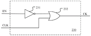
时钟门控电路230包括非门231及或门232。在时钟门控电路230中,时钟信号CK是时钟信号CLK和时钟控制信号EN的反相信号EN_a的逻辑或运算结果。The
或门232包括第一输入端、第二输入端和输出端。非门231包括输入端和输出端。或门232的第一输入端接收时钟信号CLK。或门232的第二输入端连接至非门231的输出端,经由非门231接收时钟控制信号EN的反相信号EN_a。或门232的输出端提供时钟信号CK。The OR
在本实施例中,以上升沿触发的边沿触发器为例,时钟控制信号EN以高电平表示有效状态、低电平表示无效状态为例进行说明。时钟信号CLK的每个时钟周期包括相邻上升沿之间的连续的第一电平阶段T1和第二电平阶段T2,第一电平阶段T1和第二电平阶段T2分别具有高电平和低电平。时钟信号CK提供边沿触发器110的触发边沿,边沿触发器110在触发边沿将输入数据从输入端传送至输出端。In this embodiment, an edge trigger triggered by a rising edge is taken as an example, and the clock control signal EN is described as an example where a high level indicates an active state and a low level indicates an invalid state. Each clock cycle of the clock signal CLK includes continuous first level phase T1 and second level phase T2 between adjacent rising edges, and the first level phase T1 and the second level phase T2 respectively have a high level and low level. The clock signal CK provides the triggering edge of the
在本实施例中,输入数据Di和时钟控制信号EN各自存在着相对于时钟信号边沿的信号延迟Td。信号延迟Td的最小延迟Tdmin和最大延迟Tdmax之间的区域分别采用阴影部分表示。时钟控制信号EN的信号延迟Td在最小延迟Tdmin和最大延迟Tdmax之间变化。In this embodiment, the input data Di and the clock control signal EN each have a signal delay Td relative to the edge of the clock signal. Areas between the minimum delay Tdmin and the maximum delay Tdmax of the signal delay Td are indicated by hatching, respectively. The signal delay Td of the clock control signal EN varies between a minimum delay Tdmin and a maximum delay Tdmax.
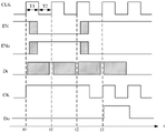
参见图7a,时钟控制信号EN的最小延迟Tdmin和最大延迟Tdmax均位于第一电平阶段T1中,时钟控制信号EN的翻转动作仅可能发生在时钟信号CLK的第一电平阶段T1中。第一电平阶段T1的开始边沿为上升沿。Referring to FIG. 7a, the minimum delay Tdmin and the maximum delay Tdmax of the clock control signal EN are both in the first level phase T1, and the inversion of the clock control signal EN can only occur in the first level phase T1 of the clock signal CLK. The starting edge of the first level stage T1 is a rising edge.
在时刻t0,时钟信号CLK到达第一个上升沿,时钟控制信号EN有效。在时刻t0开始的一个时钟周期中,时钟控制信号EN从有效状态翻转为无效状态。时钟信号CK是时钟信号CLK和反相信号EN_a的逻辑或运算结果。在时钟信号CLK的第一电平阶段T1,时钟信号CK始终为高电平。在时钟信号CLK的第二电平阶段T2,时钟信号CK始终为高电平。因此,如果时钟控制信号EN的信号延迟Td小于等于时钟信号CLK的第一电平阶段T1,则在时钟控制信号从有效状态翻转为无效状态的时钟周期中,时钟信号CK维持为高电平。At time t0, the clock signal CLK reaches the first rising edge, and the clock control signal EN is valid. In a clock cycle starting from time t0, the clock control signal EN turns from an active state to an inactive state. The clock signal CK is a logical OR operation result of the clock signal CLK and the inverted signal EN_a. In the first level phase T1 of the clock signal CLK, the clock signal CK is always at a high level. In the second level phase T2 of the clock signal CLK, the clock signal CK is always at a high level. Therefore, if the signal delay Td of the clock control signal EN is less than or equal to the first level period T1 of the clock signal CLK, the clock signal CK maintains a high level during the clock cycle when the clock control signal is switched from an active state to an inactive state.
因此,在时钟控制信号EN的信号延迟Td小于等于时钟信号CLK的第一电平阶段T1的情形下,在时刻t0开始的一个时钟周期中,时钟门控电路230屏蔽时钟信号CLK但提供时钟信号CK的上升沿,在上升沿之后经过建立时间,边沿触发器110提供的输出数据Do的信号电平与时刻t0的输入数据Di在t0时刻的信号电平一致,例如图7a所示的低电平。Therefore, in the case that the signal delay Td of the clock control signal EN is less than or equal to the first level stage T1 of the clock signal CLK, in a clock cycle starting at time t0, the
在时刻t1,时钟信号CLK到达第二个上升沿,时钟控制信号EN无效。在时刻t1开始的一个时钟周期中,时钟控制信号EN保持无效状态,如图7a所示的低电平。时钟信号CK是时钟信号CLK和反相信号EN_a的逻辑或运算结果。在这个时钟周期内,由于时钟控制信号EN一直为低,则反相信号EN_a一直为高,或运算的结果即时钟信号CK也一直为高。时钟信号CK未提供上升沿,边沿触发器110的输出数据Do的信号电平与前一时钟周期的信号电平一致,例如图7a所示的低电平。At time t1, the clock signal CLK reaches the second rising edge, and the clock control signal EN becomes invalid. In a clock cycle starting from time t1, the clock control signal EN remains in an inactive state, as shown in FIG. 7a at a low level. The clock signal CK is a logical OR operation result of the clock signal CLK and the inverted signal EN_a. During this clock cycle, since the clock control signal EN is always low, the inversion signal EN_a is always high, or the result of the operation, that is, the clock signal CK is also always high. The clock signal CK does not provide a rising edge, and the signal level of the output data Do of the
在时刻t2,时钟信号CLK到达第三个上升沿,时钟控制信号EN无效。在时刻t2开始的一个时钟周期中,时钟控制信号EN从无效状态翻转为有效状态。时钟信号CK是时钟信号CLK和反相信号EN_a的逻辑或运算结果。在时钟信号CLK的第一电平阶段T1,时钟信号CK始终为高电平。在时钟信号CLK的第二电平阶段T2,时钟信号CK始终为低电平。因此,如果时钟控制信号EN的信号延迟Td小于等于时钟信号CLK的第一电平阶段T1,则在时钟控制信号翻转的从无效状态翻转为有效状态的时钟周期中,时钟信号CK是时钟信号CLK的复制版本。At time t2, the clock signal CLK reaches the third rising edge, and the clock control signal EN becomes invalid. In a clock cycle starting from time t2, the clock control signal EN is switched from an inactive state to an active state. The clock signal CK is a logical OR operation result of the clock signal CLK and the inverted signal EN_a. In the first level phase T1 of the clock signal CLK, the clock signal CK is always at a high level. In the second level phase T2 of the clock signal CLK, the clock signal CK is always at low level. Therefore, if the signal delay Td of the clock control signal EN is less than or equal to the first level stage T1 of the clock signal CLK, the clock signal CK is the clock signal CLK in the clock cycle when the clock control signal flips from an inactive state to an active state. copied version of .
因此,在时钟控制信号EN的信号延迟Td小于等于时钟信号CLK的第一电平阶段T1的情形下,在时刻t2开始的一个时钟周期中,时钟门控电路230将时钟信号CLK复制为时钟信号CK但未提供时钟信号的上升沿,边沿触发器110的输出数据Do的信号电平与前一时钟周期的信号电平一致,例如图7a所示的低电平。Therefore, in the case where the signal delay Td of the clock control signal EN is less than or equal to the first level stage T1 of the clock signal CLK, in a clock cycle starting at time t2, the
进一步地,在时刻t3,时钟信号CLK到达第四个上升沿。时钟控制信号EN在时刻t3开始的整个时钟周期中有效,时钟信号CK是时钟信号CLK的复制版本。时钟门控电路230将时钟信号CLK复制为时钟信号CK且提供时钟信号CK的上升沿,因而可以启用边沿触发器的时钟信号和数据传输。在上升沿之后经过建立时间,边沿触发器110提供的输出数据Do的信号电平与时刻t3的输入数据Di的信号电平一致,即,高电平。在时刻t3之后,时钟控制信号EN可以持续有效,时钟信号CK是时钟信号CLK的复制版本,时钟信号CLK跳变时,边沿触发器110在所述第二时钟信号的触发边沿,接收所述数据输入端的输入数据并传送至所述数据输出端。Further, at time t3, the clock signal CLK reaches the fourth rising edge. The clock control signal EN is valid for the entire clock cycle starting at time t3, and the clock signal CK is a replica version of the clock signal CLK. The
参见图7b,时钟控制信号EN的最小延迟Tdmin和最大延迟Tdmax均位于第二电平阶段T2中,时钟控制信号EN的翻转动作仅可能发生在时钟信号CLK的第二电平阶段T2中。第二电平阶段T2的开始边沿为下降沿。Referring to FIG. 7b, the minimum delay Tdmin and the maximum delay Tdmax of the clock control signal EN are both in the second level phase T2, and the inversion of the clock control signal EN can only occur in the second level phase T2 of the clock signal CLK. The start edge of the second level phase T2 is a falling edge.
在时刻t0,时钟信号CLK到达第一个上升沿,时钟控制信号EN有效。在时刻t0开始的一个时钟周期中,时钟控制信号EN从有效状态翻转为无效状态。时钟信号CK是时钟信号CLK和反相信号EN_a的逻辑或运算结果。在时钟信号CLK的第一电平阶段T1,时钟信号CK始终为高电平。在时钟信号CLK的第二电平阶段T2,时钟信号CK的信号电平与时钟控制信号EN的信号延迟相关。如果时钟控制信号EN的信号延迟Td大于时钟信号CLK的第一电平阶段T1,则在时钟信号CLK的第二电平阶段T2,时钟信号CK在第二电平阶段T2的开始时刻从高电平翻转为低电平,在第二电平阶段T2中的时刻ta之后的某个时刻从低电平翻转为高电平且还可能存在反复跳变,因而产生毛刺。At time t0, the clock signal CLK reaches the first rising edge, and the clock control signal EN is valid. In a clock cycle starting from time t0, the clock control signal EN turns from an active state to an inactive state. The clock signal CK is a logical OR operation result of the clock signal CLK and the inverted signal EN_a. In the first level phase T1 of the clock signal CLK, the clock signal CK is always at a high level. In the second level phase T2 of the clock signal CLK, the signal level of the clock signal CK is related to the signal delay of the clock control signal EN. If the signal delay Td of the clock control signal EN is greater than the first level stage T1 of the clock signal CLK, then in the second level stage T2 of the clock signal CLK, the clock signal CK starts from the high voltage at the beginning of the second level stage T2 The level flips to a low level, and at a certain time after the time ta in the second level stage T2, it flips from a low level to a high level and there may be repeated jumps, thus generating glitches.
因此,在时钟控制信号EN的信号延迟Td大于时钟信号CLK的第一电平阶段T1的情形下,在时刻t0开始的一个时钟周期中,时钟门控电路230产生的时钟信号CK出现毛刺。毛刺提供了随时钟控制信号EN变化的附加上升沿,边沿触发器110在附加上升沿之后经过建立时间提供的输出数据Do的信号电平与输入数据Di在附加上升沿的信号电平一致。一方面,边沿触发器110的输入数据Di由于自身的信号延迟存在着不确定状态,另一方面,时钟信号CK的毛刺提供的附加上升沿与输入数据Di的不确定状态重叠。因此,在附加上升沿之后经过建立时间,边沿触发器110的提供的输出数据Do与附加上升沿的信号电平一致,例如图7b的不确定状态。Therefore, when the signal delay Td of the clock control signal EN is greater than the first level stage T1 of the clock signal CLK, a glitch occurs in the clock signal CK generated by the
在时刻t1,时钟信号CLK到达第二个上升沿,时钟控制信号EN无效。与图7a相同,在时刻t1开始的一个时钟周期中,时钟信号CK维持为高电平,既未提供上升沿也未提供下降沿。边沿触发器110的输出数据Do的信号电平与前一时钟周期的信号电平一致,例如图7b所示的不确定状态。At time t1, the clock signal CLK reaches the second rising edge, and the clock control signal EN becomes invalid. Same as in FIG. 7 a , in a clock cycle starting from time t1 , the clock signal CK remains at a high level, and neither a rising edge nor a falling edge is provided. The signal level of the output data Do of the
在时刻t2,时钟信号CLK到达第三个上升沿,时钟控制信号EN无效。在时刻t2开始的一个时钟周期中,时钟控制信号EN从无效状态翻转为有效状态。时钟信号CK是时钟信号CLK和反相信号EN_a的逻辑或运算结果。在时钟信号CLK的第一电平阶段T1,时钟信号CK始终为高电平。在时钟信号CLK的第二电平阶段T2,时钟信号CK的信号电平与时钟控制信号EN的信号延迟相关。如果时钟控制信号EN的信号延迟Td大于时钟信号CLK的第一电平阶段T1,则在时钟信号CLK的第二电平阶段T2,与时钟控制信号EN的翻转时刻相同,时钟信号CK从高电平状态翻转为低电平状态,因而产生毛刺。At time t2, the clock signal CLK reaches the third rising edge, and the clock control signal EN becomes invalid. In a clock cycle starting from time t2, the clock control signal EN is switched from an inactive state to an active state. The clock signal CK is a logical OR operation result of the clock signal CLK and the inverted signal EN_a. In the first level phase T1 of the clock signal CLK, the clock signal CK is always at a high level. In the second level phase T2 of the clock signal CLK, the signal level of the clock signal CK is related to the signal delay of the clock control signal EN. If the signal delay Td of the clock control signal EN is greater than the first level phase T1 of the clock signal CLK, then in the second level phase T2 of the clock signal CLK, which is the same as the inversion time of the clock control signal EN, the clock signal CK changes from a high level to The flat state flips to a low state, thus generating a glitch.
因此,在时钟控制信号EN的信号延迟Td大于时钟信号CLK的第一电平阶段T1的情形下,在时刻t2开始的一个时钟周期中,时钟门控电路230产生的时钟信号CK出现毛刺。然而,毛刺仅能提供随时钟控制信号EN变化的附加下降沿,且可能由于跳变而提供边沿触发器110的触发边沿。因此,边沿触发器110的输出数据Do的信号电平与前一时钟周期的信号电平一致,例如图7b所示的不确定状态。Therefore, when the signal delay Td of the clock control signal EN is greater than the first level stage T1 of the clock signal CLK, a glitch occurs in the clock signal CK generated by the
进一步地,在时刻t3,时钟信号CLK到达第四个上升沿。时钟控制信号EN在时刻t3开始的整个时钟周期中有效,时钟信号CK是时钟信号CLK的复制版本。时钟门控电路230将时钟信号CLK复制为时钟信号CK且提供时钟信号CK的上升沿,因而可以启用边沿触发器的时钟信号和数据传输。在上升沿之后经过建立时间,边沿触发器110提供的输出数据Do的信号电平与时刻t3的输入数据Di的信号电平一致,即,高电平。在时刻t3之后,时钟控制信号EN可以持续有效,时钟信号CK是时钟信号CLK的复制版本,时钟信号CLK跳变时,边沿触发器110在所述第二时钟信号的触发边沿,接收所述数据输入端的输入数据并传送至所述数据输出端。Further, at time t3, the clock signal CLK reaches the fourth rising edge. The clock control signal EN is valid for the entire clock cycle starting at time t3, and the clock signal CK is a replica version of the clock signal CLK. The
上述的时钟门控电路230在时钟控制信号EN的不同延迟条件下具有不同的电路特性。在时钟控制信号EN的最小延迟Tdmin和最大延迟Tdmax均位于第一电平阶段T1中、且第一电平阶段T1的开始边沿为上升沿的条件下,选择图6所示的时钟门控电路230,以替代图4所示的时钟门控电路130。The aforementioned
在时钟控制信号EN维持有效的时钟周期中,时钟门控电路230将时钟信号CLK复制为时钟信号CK,时钟信号CK提供至边沿触发器110的时钟输入端,在时钟控制信号EN维持无效的时钟周期中,时钟门控电路230屏蔽时钟信号CLK。因此,采用时钟门控电路230可以禁用边沿触发器110的时钟翻转和数据传输。In the clock period when the clock control signal EN is kept valid, the
在时钟控制信号EN从有效状态翻转至无效状态的时钟周期中,时钟门控电路230屏蔽时钟信号CLK,以及将时钟信号CK维持为预定电平。此时,时钟信号CK仍然提供边沿触发器110的触发边沿,时钟门控电路230允许边沿触发器110的数据传输,边沿触发器110提供的输出数据Do为当前触发边沿的输入数据Di。时钟门控电路230禁用边沿触发器110的时钟翻转,因而可以降低边沿触发器110因时钟信号CK翻转产生的动态功耗。During the clock period when the clock control signal EN is switched from an active state to an inactive state, the
在时钟控制信号EN从无效状态翻转至有效状态的时钟周期中,时钟门控电路230将时钟信号CLK复制为时钟信号CK,因而允许边沿触发器110的时钟翻转。此时,时钟信号CK未能提供边沿触发器110的触发边沿,时钟门控电路230禁用边沿触发器110的数据传输,边沿触发器110维持前一触发边沿的输入数据Di,因而可以降低边沿触发器110因数据传输产生的动态功耗。During the clock cycle when the clock control signal EN toggles from an inactive state to an active state, the
时钟门控电路230对时钟控制信号EN的时序要求是时钟控制信号EN的翻转发生在时钟信号CLK的一个时钟周期的触发边沿之后的电平阶段,本例中为第一电平阶段T1。如果希望在预定时刻禁用数据传输,则在预定时刻之前的最后一个整时钟周期的第一电平阶段T1内完成时钟控制信号EN从有效状态至无效状态的翻转动作,在预定时刻开始的最后一个时钟周期的时钟信号CLK的第一电平阶段T1内完成时钟控制信号EN从无效状态至有效状态的翻转动作。The timing requirement of the
与图4所示的时钟门控电路130相比,根据本实施例的时钟门控电路230省去了锁存器,时钟门控电路230使用的硬件逻辑较少,并且自身的工作功耗较低。在触发单元中,任意数量的边沿触发器110可以共用时钟门控电路230从而组成触发器组。对于触发器组包含任意数量的边沿触发器110的情形,因时钟门控电路230本身的功耗而增加的功耗远小于边沿触发器110因时钟门控而减少的功耗,因此,触发单元始终可以实现功耗降低。Compared with the
图8示出根据本发明第二实施例的时钟门控电路的示意性电路图。参见图3,时钟门控电路330和边沿触发器110共同组成触发单元,时钟门控电路330向边沿触发器110提供时钟信号CK。FIG. 8 shows a schematic circuit diagram of a clock gating circuit according to a second embodiment of the present invention. Referring to FIG. 3 , the
时钟门控电路330包括与门331。在时钟门控电路330中,时钟信号CK是时钟信号CLK和时钟控制信号EN的逻辑与运算结果。The
与门331包括第一输入端、第二输入端和输出端。与门331的第一输入端接收时钟信号CLK,第二输入端接时钟控制信号EN,输出端提供时钟信号CK。The AND
在本实施例中,以下降沿触发的边沿触发器为例,时钟控制信号EN以高电平表示有效状态、低电平表示无效状态为例进行说明。时钟信号CLK的每个时钟周期包括相邻下降沿之间的连续的第一电平阶段T1和第二电平阶段T2,第一电平阶段T1和第二电平阶段T2分别具有低电平和高电平。时钟信号CK提供边沿触发器110的触发边沿,边沿触发器110在触发边沿将输入数据从输入端传送至输出端。In this embodiment, an edge trigger triggered by a falling edge is taken as an example, and the clock control signal EN is described as an example where a high level indicates an active state and a low level indicates an invalid state. Each clock cycle of the clock signal CLK includes continuous first level phase T1 and second level phase T2 between adjacent falling edges, and the first level phase T1 and the second level phase T2 respectively have a low level and high level. The clock signal CK provides the triggering edge of the
在本实施例中,输入数据Di和时钟控制信号EN各自存在着相对于时钟信号边沿的信号延迟Td。信号延迟Td的最小延迟Tdmin和最大延迟Tdmax之间的区域分别采用阴影部分表示。时钟控制信号EN的信号延迟Td在最小延迟Tdmin和最大延迟Tdmax之间变化。In this embodiment, the input data Di and the clock control signal EN each have a signal delay Td relative to the edge of the clock signal. Areas between the minimum delay Tdmin and the maximum delay Tdmax of the signal delay Td are indicated by hatching, respectively. The signal delay Td of the clock control signal EN varies between a minimum delay Tdmin and a maximum delay Tdmax.
参见图9a,时钟控制信号EN的最小延迟Tdmin和最大延迟Tdmax均位于第一电平阶段T1中,时钟控制信号EN的翻转动作仅可能发生在时钟信号CLK的第一电平阶段T1中。第一电平阶段T1的开始边沿为下降沿。Referring to FIG. 9a, the minimum delay Tdmin and the maximum delay Tdmax of the clock control signal EN are both in the first level phase T1, and the inversion of the clock control signal EN can only occur in the first level phase T1 of the clock signal CLK. The starting edge of the first level stage T1 is a falling edge.
在时刻t0,时钟信号CLK到达第一个下降沿,时钟控制信号EN有效。在时刻t0开始的一个时钟周期中,时钟控制信号EN从有效状态翻转为无效状态。时钟信号CK是时钟信号CLK和时钟控制信号EN的逻辑与运算结果。在时钟信号CLK的第一电平阶段T1,时钟信号CK始终为低电平。在时钟信号CLK的第二电平阶段T2,时钟信号CK始终为低电平。因此,如果时钟控制信号EN的信号延迟Td小于等于时钟信号CLK的第一电平阶段T1,则在时钟控制信号从有效状态翻转为无效状态的时钟周期中,时钟信号CK维持为低电平。At time t0, the clock signal CLK reaches the first falling edge, and the clock control signal EN is valid. In a clock cycle starting from time t0, the clock control signal EN turns from an active state to an inactive state. The clock signal CK is a logical AND operation result of the clock signal CLK and the clock control signal EN. In the first level phase T1 of the clock signal CLK, the clock signal CK is always at low level. In the second level phase T2 of the clock signal CLK, the clock signal CK is always at low level. Therefore, if the signal delay Td of the clock control signal EN is less than or equal to the first level period T1 of the clock signal CLK, the clock signal CK maintains a low level during the clock period when the clock control signal turns from an active state to an inactive state.
因此,在时钟控制信号EN的信号延迟Td小于等于时钟信号CLK的第一电平阶段T1的情形下,在时刻t0开始的一个时钟周期中,时钟门控电路330屏蔽时钟信号CLK但提供时钟信号CK的下降沿,在下降沿之后经过建立时间,边沿触发器110提供的输出数据Do的信号电平与时刻t0的输入数据Di在t0时刻的信号电平一致,例如图9a所示的低电平。Therefore, in the case where the signal delay Td of the clock control signal EN is less than or equal to the first level stage T1 of the clock signal CLK, in a clock cycle starting at time t0, the
在时刻t1,时钟信号CLK到达第二个下降沿,时钟控制信号EN无效。在时刻t1开始的一个时钟周期中,时钟控制信号EN保持无效状态,如图9a所示的低电平。时钟信号CK是时钟信号CLK和时钟控制信号EN的逻辑与运算结果。在这个时钟周期内,由于时钟控制信号EN一直为低,与运算的结果即时钟信号CK也一直为低。时钟信号CK未提供下降沿,边沿触发器110的输出数据Do的信号电平与前一时钟周期的信号电平一致,例如图9a所示的低电平。At time t1, the clock signal CLK reaches the second falling edge, and the clock control signal EN becomes invalid. In a clock cycle starting from time t1, the clock control signal EN remains in an inactive state, as shown in FIG. 9a at a low level. The clock signal CK is a logical AND operation result of the clock signal CLK and the clock control signal EN. During this clock cycle, since the clock control signal EN is always low, the result of the AND operation, that is, the clock signal CK is also always low. The clock signal CK does not provide a falling edge, and the signal level of the output data Do of the
在时刻t2,时钟信号CLK到达第三个下降沿,时钟控制信号EN无效。在时刻t2开始的一个时钟周期中,时钟控制信号EN从无效状态翻转为有效状态。时钟信号CK是时钟信号CLK和时钟控制信号EN的逻辑与运算结果。在时钟信号CLK的第一电平阶段T1,时钟信号CK始终为低电平。在时钟信号CLK的第二电平阶段T2,时钟信号CK始终为高电平。因此,如果时钟控制信号EN的信号延迟Td小于等于时钟信号CLK的第一电平阶段T1,则在时钟控制信号从无效状态翻转为有效状态的时钟周期中,时钟信号CK是时钟信号CLK的复制版本。At time t2, the clock signal CLK reaches the third falling edge, and the clock control signal EN becomes invalid. In a clock cycle starting from time t2, the clock control signal EN is switched from an inactive state to an active state. The clock signal CK is a logical AND operation result of the clock signal CLK and the clock control signal EN. In the first level phase T1 of the clock signal CLK, the clock signal CK is always at low level. In the second level phase T2 of the clock signal CLK, the clock signal CK is always at a high level. Therefore, if the signal delay Td of the clock control signal EN is less than or equal to the first level stage T1 of the clock signal CLK, the clock signal CK is a copy of the clock signal CLK during the clock cycle when the clock control signal is turned from an inactive state to an active state. Version.
因此,在时钟控制信号EN的信号延迟Td小于等于时钟信号CLK的第一电平阶段T1的情形下,在时刻t2开始的一个时钟周期中,时钟门控电路330将时钟信号CLK复制为时钟信号CK但未提供时钟信号的下降沿,边沿触发器110的输出数据Do的信号电平与前一时钟周期的信号电平一致,例如图9a所示的低电平。Therefore, in the case where the signal delay Td of the clock control signal EN is less than or equal to the first level stage T1 of the clock signal CLK, in a clock cycle starting at time t2, the
进一步地,在时刻t3,时钟信号CLK到达第四个下降沿。时钟控制信号EN在时刻t3开始的整个时钟周期中有效,时钟信号CK是时钟信号CLK的复制版本。时钟门控电路330将时钟信号CLK复制为时钟信号CK且提供时钟信号CK的下降沿,因而可以启用边沿触发器的时钟信号和数据传输。在下降沿之后经过建立时间,边沿触发器110提供的输出数据Do的信号电平与时刻t3的输入数据Di的信号电平一致,即,高电平。在时刻t3之后,时钟控制信号EN可以持续有效,时钟信号CK是时钟信号CLK的复制版本,时钟信号CLK跳变时,边沿触发器110在所述第二时钟信号的触发边沿,接收所述数据输入端的输入数据并传送至所述数据输出端。Further, at time t3, the clock signal CLK reaches the fourth falling edge. The clock control signal EN is valid for the entire clock cycle starting at time t3, and the clock signal CK is a replica version of the clock signal CLK. The
参见图9b,时钟控制信号EN的最小延迟Tdmin和最大延迟Tdmax均位于第二电平阶段T2中,时钟控制信号EN的翻转动作仅可能发生在时钟信号CLK的第二电平阶段T2中。第二电平阶段T2的开始边沿为上升沿。Referring to FIG. 9b, the minimum delay Tdmin and the maximum delay Tdmax of the clock control signal EN are both in the second level phase T2, and the inversion of the clock control signal EN can only occur in the second level phase T2 of the clock signal CLK. The start edge of the second level phase T2 is a rising edge.
在时刻t0,时钟信号CLK到达第一个下降沿,时钟控制信号EN有效。在时刻t0开始的一个时钟周期中,时钟控制信号EN从有效状态翻转为无效状态。时钟信号CK是时钟信号CLK和时钟控制信号EN的逻辑与运算结果。在时钟信号CLK的第一电平阶段T1,时钟信号CK始终为低电平。在时钟信号CLK的第二电平阶段T2,时钟信号CK的信号电平与时钟控制信号EN的信号延迟相关。如果时钟控制信号EN的信号延迟Td大于时钟信号CLK的第一电平阶段T1,则在时钟信号CLK的第二电平阶段T2,时钟信号CK在第二电平阶段T2的开始时刻从低电平翻转为高电平,在第二电平阶段T2中的时刻ta之后的某个时刻从高电平翻转为低电平且可能存在跳变,因而产生毛刺。At time t0, the clock signal CLK reaches the first falling edge, and the clock control signal EN is valid. In a clock cycle starting from time t0, the clock control signal EN turns from an active state to an inactive state. The clock signal CK is a logical AND operation result of the clock signal CLK and the clock control signal EN. In the first level phase T1 of the clock signal CLK, the clock signal CK is always at low level. In the second level phase T2 of the clock signal CLK, the signal level of the clock signal CK is related to the signal delay of the clock control signal EN. If the signal delay Td of the clock control signal EN is greater than the first level phase T1 of the clock signal CLK, then in the second level phase T2 of the clock signal CLK, the clock signal CK starts from low power at the beginning of the second level phase T2 The level flips to a high level, and at a certain time after the time ta in the second level stage T2, it flips from a high level to a low level and there may be a jump, thus generating a glitch.
因此,在时钟控制信号EN的信号延迟Td大于时钟信号CLK的第一电平阶段T1的情形下,在时刻t0开始的一个时钟周期中,时钟门控电路330产生的时钟信号CK出现毛刺。毛刺提供了随时钟控制信号EN变化的附加下降沿,边沿触发器110在附加下降沿之后经过建立时间提供的输出数据Do的信号电平与输入数据Di在附加下降沿的信号电平一致。一方面,边沿触发器110的输入数据Di由于自身的信号延迟存在着不确定状态,另一方面,时钟信号CK的毛刺提供的附加下降沿与输入数据Di的不确定状态重叠。因此,在附加下降沿之后经过建立时间,边沿触发器110的提供的输出数据Do与附加下降沿的信号电平一致,例如图9b的不确定状态。Therefore, when the signal delay Td of the clock control signal EN is greater than the first level stage T1 of the clock signal CLK, a glitch occurs in the clock signal CK generated by the
在时刻t1,时钟信号CLK到达第二个下降沿,时钟控制信号EN无效。与图9a相同,在时刻t1开始的一个时钟周期中,时钟信号CK维持为低电平,既未提供上升沿也未提供下降沿。边沿触发器110的输出数据Do的信号电平与前一时钟周期的信号电平一致,例如图9b所示的不确定状态。At time t1, the clock signal CLK reaches the second falling edge, and the clock control signal EN becomes invalid. Same as in FIG. 9 a , in a clock cycle starting from time t1 , the clock signal CK is maintained at a low level, and neither a rising edge nor a falling edge is provided. The signal level of the output data Do of the
在时刻t2,时钟信号CLK到达第三个下降沿,时钟控制信号EN无效。在时刻t2开始的一个时钟周期中,时钟控制信号EN从无效状态翻转为有效状态。时钟信号CK是时钟信号CLK和时钟控制信号EN的逻辑与运算结果。在时钟信号CLK的第一电平阶段T1,时钟信号CK始终为低电平。在时钟信号CLK的第二电平阶段T2,时钟信号CK的信号电平与时钟控制信号EN的信号延迟相关。如果时钟控制信号EN的信号延迟Td大于时钟信号CLK的第一电平阶段T1,则在时钟信号CLK的第二电平阶段T2,与时钟控制信号EN的翻转时刻相同,时钟信号CK从低电平状态翻转为高电平状态,因而产生毛刺。At time t2, the clock signal CLK reaches the third falling edge, and the clock control signal EN becomes invalid. In a clock cycle starting from time t2, the clock control signal EN is switched from an inactive state to an active state. The clock signal CK is a logical AND operation result of the clock signal CLK and the clock control signal EN. In the first level phase T1 of the clock signal CLK, the clock signal CK is always at low level. In the second level phase T2 of the clock signal CLK, the signal level of the clock signal CK is related to the signal delay of the clock control signal EN. If the signal delay Td of the clock control signal EN is greater than the first level phase T1 of the clock signal CLK, then in the second level phase T2 of the clock signal CLK, which is the same as the inversion time of the clock control signal EN, the clock signal CK changes from a low level to The flat state flips to a high state, thus generating a glitch.
因此,在时钟控制信号EN的信号延迟Td大于时钟信号CLK的第一电平阶段T1的情形下,在时刻t2开始的一个时钟周期中,时钟门控电路330产生的时钟信号CK出现毛刺。然而,毛刺仅能提供随时钟控制信号EN变化的附加上升沿,且可能由于跳变而提供边沿触发器110的触发边沿。因此,边沿触发器110的输出数据Do的信号电平与前一时钟周期的信号电平一致,例如图9b所示的不确定状态。Therefore, when the signal delay Td of the clock control signal EN is greater than the first level stage T1 of the clock signal CLK, a glitch occurs in the clock signal CK generated by the
进一步地,在时刻t3,时钟信号CLK到达第四个下降沿。时钟控制信号EN在时刻t3开始的整个时钟周期中有效,时钟信号CK是时钟信号CLK的复制版本。时钟门控电路330将时钟信号CLK复制为时钟信号CK且提供时钟信号CK的下降沿,因而可以启用边沿触发器的时钟信号和数据传输。在下降沿之后经过建立时间,边沿触发器110提供的输出数据Do的信号电平与时刻t3的输入数据Di的信号电平一致,即,高电平。在时刻t3之后,时钟控制信号EN可以持续有效,时钟信号CK是时钟信号CLK的复制版本,时钟信号CLK跳变时,边沿触发器110在所述第二时钟信号的触发边沿,接收所述数据输入端的输入数据并传送至所述数据输出端。Further, at time t3, the clock signal CLK reaches the fourth falling edge. The clock control signal EN is valid for the entire clock cycle starting at time t3, and the clock signal CK is a replica version of the clock signal CLK. The
上述的时钟门控电路330在时钟控制信号EN的不同延迟条件下具有不同的电路特性。在时钟控制信号EN的最小延迟Tdmin和最大延迟Tdmax均位于第一电平阶段T1中、且第一电平阶段T1的开始边沿为下降沿的条件下,选择图8所示的时钟门控电路330,以替代图4所示的时钟门控电路130。The aforementioned
在时钟控制信号EN维持有效的时钟周期中,时钟门控电路330将时钟信号CLK复制为时钟信号CK,时钟信号CK提供至边沿触发器110的时钟输入端,在时钟控制信号EN维持无效的时钟周期中,时钟门控电路330屏蔽时钟信号CLK。因此,采用时钟门控电路330可以禁用边沿触发器110的时钟翻转和数据传输。During the clock period when the clock control signal EN remains valid, the
在时钟控制信号EN从有效状态翻转至无效状态的时钟周期中,时钟门控电路330屏蔽时钟信号CLK,以及将时钟信号CK维持为预定电平。此时,时钟信号CK仍然提供边沿触发器110的触发边沿,时钟门控电路330允许边沿触发器110的数据传输,边沿触发器110提供的输出数据Do为当前触发边沿的输入数据Di。时钟门控电路330禁用边沿触发器110的时钟翻转,因而可以降低边沿触发器110因时钟信号CK翻转产生的动态功耗。。During the clock period when the clock control signal EN is switched from an active state to an inactive state, the
在时钟控制信号EN从无效状态翻转至有效状态的时钟周期中,时钟门控电路330将时钟信号CLK复制为时钟信号CK,因而允许边沿触发器110的时钟翻转。此时,时钟信号CK未能提供边沿触发器110的触发边沿,时钟门控电路330禁用边沿触发器110的数据传输,边沿触发器110维持前一触发边沿的输入数据Di,因而可以降低边沿触发器110因数据传输产生的动态功耗。During the clock cycle when the clock control signal EN toggles from an inactive state to an active state, the
时钟门控电路330对时钟控制信号EN的时序要求是时钟控制信号EN的翻转发生在时钟信号CLK的一个时钟周期的触发边沿之后的电平阶段,本例中为第一电平阶段T1。如果希望在预定时刻禁用数据传输,则在预定时刻之前的最后一个整时钟周期的第一电平阶段T1内完成时钟控制信号EN从有效状态至无效状态的翻转动作,在预定时刻开始的最后一个时钟周期的时钟信号CLK的第一电平阶段T1内完成时钟控制信号EN从无效状态至有效状态的翻转动作。The timing requirement of the
与图4所示的时钟门控电路130相比,根据本实施例的时钟门控电路330省去了锁存器,时钟门控电路330使用的硬件逻辑较少,并且自身的工作功耗较低。在触发单元中,任意数量的边沿触发器110可以共用时钟门控电路330从而组成触发器组。对于触发器组包含任意数量的边沿触发器110的情形,因时钟门控电路330本身的功耗而增加的功耗远小于边沿触发器110因时钟门控而减少的功耗,因此,触发单元始终可以实现功耗降低。Compared with the
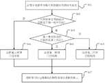
图10示出根据本发明第三实施例的触发单元设计方法的流程图。FIG. 10 shows a flowchart of a trigger unit design method according to a third embodiment of the present invention.
该触发单元设计方法包括步骤S01至S07。The trigger unit design method includes steps S01 to S07.
在步骤S01中,在数字电路中分析时钟控制信号EN的信号延迟Td。In step S01, the signal delay Td of the clock control signal EN is analyzed in the digital circuit.
时钟控制信号EN的信号延迟为数字电路产生时钟控制信号时从时钟边沿开始运算至时钟控制信号的翻转稳定所需的运算耗时。现有的EDA工具大都可以获得时钟控制信号EN的信号延迟Td。该信号延迟Td例如在最小延迟Tdmin和最大延迟Tdmax的范围内变化。The signal delay of the clock control signal EN is the time-consuming operation required from the clock edge to the inversion and stabilization of the clock control signal when the digital circuit generates the clock control signal. Most of the existing EDA tools can obtain the signal delay Td of the clock control signal EN. The signal delay Td varies, for example, within the range of a minimum delay Tdmin and a maximum delay Tdmax.
然后,根据时钟控制信号EN的信号延迟Td,从多个不同类型的时钟门控电路中选择边沿触发器的时钟门控电路。Then, according to the signal delay Td of the clock control signal EN, the clock gating circuit of the edge trigger is selected from a plurality of different types of clock gating circuits.
根据时钟控制信号EN的信号延迟Td,在若干不同类型的时钟门控电路中进行选择,多个不同类型的时钟门控电路组合应用,实现更优的低功耗方案。时钟门控电路对时钟控制信号EN和时钟信号CLK进行逻辑运算以产生时钟信号CK。According to the signal delay Td of the clock control signal EN, several different types of clock gating circuits are selected, and multiple different types of clock gating circuits are used in combination to achieve a better low power consumption solution. The clock gating circuit performs logic operations on the clock control signal EN and the clock signal CLK to generate the clock signal CK.
时钟信号CLK的每个时钟周期包括连续的第一电平阶段T1和第二电平阶段T2,第一电平阶段T1和第二电平阶段T2分别具有彼此反相的第一电平和第二电平。在第一电平为高电平的情形下,第一电平阶段T1的开始边沿为上升沿,在第一电平为低电平的情形下,第一电平阶段T1的开始边沿为下降沿。Each clock period of the clock signal CLK includes a continuous first level phase T1 and a second level phase T2, and the first level phase T1 and the second level phase T2 respectively have the first level and the second level which are opposite to each other. level. When the first level is high, the start edge of the first level stage T1 is a rising edge, and when the first level is low, the start edge of the first level stage T1 is a falling edge along.
在步骤S02中,判断时钟控制信号的延迟范围是否位于第一电平阶段。In step S02, it is judged whether the delay range of the clock control signal is in the first level stage.
在该步骤中,根据时钟控制信号EN的延迟范围类型选择所述第一时钟门控电路和所述第二时钟门控电路之一。In this step, one of the first clock gating circuit and the second clock gating circuit is selected according to the delay range type of the clock control signal EN.
时钟控制信号EN的信号延迟Td在最小延迟Tdmin和最大延迟Tdmax之间变化。将时钟控制信号EN的最小延迟Tdmin和最大延迟Tdmax与时钟信号CLK的第一电平阶段T1进行比较,以判断时钟信号EN的延迟范围是否位于第一电平阶段。The signal delay Td of the clock control signal EN varies between a minimum delay Tdmin and a maximum delay Tdmax. The minimum delay Tdmin and the maximum delay Tdmax of the clock control signal EN are compared with the first level stage T1 of the clock signal CLK to determine whether the delay range of the clock signal EN is in the first level stage.
如果时钟控制信号EN的信号延迟Td符合以下条件:Tdmin<T1,Tdmax<T1,则时钟控制信号EN的延迟范围位于第一电平阶段中。此时,时钟控制信号EN的翻转动作只可能发生在时钟信号CLK的单个电平阶段。进一步地,执行步骤S03,选择如图6所示的第一时钟门控电路和如图8所示的第二时钟门控电路之一。If the signal delay Td of the clock control signal EN meets the following conditions: Tdmin<T1, Tdmax<T1, then the delay range of the clock control signal EN is in the first level stage. At this time, the inversion action of the clock control signal EN can only occur in a single level phase of the clock signal CLK. Further, step S03 is executed to select one of the first clock gating circuit shown in FIG. 6 and the second clock gating circuit shown in FIG. 8 .
如果时钟控制信号EN的信号延迟Td符合以下条件:Tdmin<T1,Tdmax>T1,则,时钟控制信号EN的延迟范围包括第一电平阶段和第二电平阶段彼此相邻的时间段。此时,时钟控制信号EN的翻转动作可能发生在时钟信号CLK的任意电平阶段。进一步地,执行步骤S06,选择如图4所示的第三时钟门控电路。If the signal delay Td of the clock control signal EN satisfies the following condition: Tdmin<T1, Tdmax>T1, then the delay range of the clock control signal EN includes a time period in which the first level stage and the second level stage are adjacent to each other. At this time, the inversion action of the clock control signal EN may occur at any level stage of the clock signal CLK. Further, step S06 is executed to select the third clock gating circuit as shown in FIG. 4 .
在步骤S03中,进一步地,判断第一电平阶段的开始边沿类型。In step S03, further, determine the type of the start edge of the first level stage.
在该步骤中,根据第一电平阶段T1的开始边沿类型选择所述第一时钟门控电路和所述第二时钟门控电路之一。In this step, one of the first clock gating circuit and the second clock gating circuit is selected according to the start edge type of the first level phase T1.
如果第一电平阶段T1的开始边沿为上升沿,则执行步骤S04,选择如图6所示的第一时钟门控电路。If the start edge of the first level stage T1 is a rising edge, step S04 is executed to select the first clock gating circuit as shown in FIG. 6 .
如上所述,在图6所示的时钟门控电路中,在时钟控制信号EN从有效状态翻转至无效状态的时钟周期,时钟门控电路的时钟信号CK屏蔽时钟信号CLK但提供时钟信号CK的上升沿。在时钟控制信号EN从无效状态翻转至有效状态的时钟周期,时钟门控电路将时钟信号CLK复制为时钟信号CK但未提供时钟时钟信号的上升沿。因此,只要时钟控制信号EN在时钟信号CLK的第一电平阶段T1翻转且第一电平阶段T1的开始边沿为上升沿,就可以消除边沿触发器的时钟信号的毛刺,使得边沿触发器可以正常工作。As mentioned above, in the clock gating circuit shown in FIG. 6, the clock signal CK of the clock gating circuit shields the clock signal CLK but provides the rising edge. During the clock period when the clock control signal EN is turned from an inactive state to an active state, the clock gating circuit replicates the clock signal CLK as the clock signal CK but does not provide a rising edge of the clock signal. Therefore, as long as the clock control signal EN is inverted in the first level phase T1 of the clock signal CLK and the start edge of the first level phase T1 is a rising edge, the glitch of the clock signal of the edge trigger can be eliminated, so that the edge trigger can normal work.
如果第一电平阶段T1的开始边沿为下降沿,则执行步骤S05,选择如图8所示的第二时钟门控电路。If the start edge of the first level stage T1 is a falling edge, step S05 is executed to select the second clock gating circuit as shown in FIG. 8 .
如上所述,在图8所示的时钟门控电路中,在时钟控制信号EN从有效状态翻转至无效状态的时钟周期,时钟门控电路的时钟信号CK屏蔽时钟信号CLK但提供时钟信号CK的下降沿。在时钟控制信号EN从无效状态翻转至有效状态的时钟周期,时钟门控电路将时钟信号CLK复制为时钟信号CK但未提供时钟时钟信号的下降沿。因此,只要时钟控制信号EN在时钟信号CLK的第一电平阶段T1翻转且第一电平阶段T1的开始边沿为下降沿,就可以消除边沿触发器的时钟信号的毛刺,使得边沿触发器可以正常工作。As mentioned above, in the clock gating circuit shown in FIG. 8, the clock signal CK of the clock gating circuit shields the clock signal CLK but provides the falling edge. During the clock period when the clock control signal EN is turned from an inactive state to an active state, the clock gating circuit replicates the clock signal CLK as the clock signal CK but does not provide a falling edge of the clock signal. Therefore, as long as the clock control signal EN is inverted in the first level phase T1 of the clock signal CLK and the start edge of the first level phase T1 is a falling edge, the glitch of the clock signal of the edge trigger can be eliminated, so that the edge trigger can normal work.
在步骤S06中,选择如图4所示的第三时钟门控电路。In step S06, the third clock gating circuit as shown in FIG. 4 is selected.
如上所述,图4所示的时钟门控电路包含锁存器,无论时钟控制信号EN在时钟信号CLK的第一电平阶段T1翻转还是在第二电平阶段T2翻转,均可以消除边沿触发器的时钟信号的毛刺,使得边沿触发器可以正常工作。As mentioned above, the clock gating circuit shown in Figure 4 includes a latch, which can eliminate the edge trigger regardless of whether the clock control signal EN is inverted in the first level phase T1 of the clock signal CLK or in the second level phase T2. The glitch of the clock signal of the device makes the edge trigger work normally.
在步骤S07中,将至少一个边沿触发器和选择的时钟门控电路组合成触发单元。In step S07, at least one edge trigger and the selected clock gating circuit are combined into a trigger unit.
例如,将所述选择的时钟门控电路的输出端连接至至少一个边沿触发器的时钟输入端以组合成触发单元。For example, the output terminal of the selected clock gating circuit is connected to the clock input terminal of at least one edge trigger to form a trigger unit.
图11示出在图10所示的触发单元设计方法中时钟门控电路和边沿触发器的一种组合方法。FIG. 11 shows a combination method of a clock gating circuit and an edge trigger in the trigger unit design method shown in FIG. 10 .
以如图6所示的第一时钟门控电路为例进行说明。第一时钟门控电路在时钟控制信号EN从有效状态翻转至无效状态的时钟周期,时钟门控电路的时钟信号CK屏蔽时钟信号CLK但提供时钟信号CK的上升沿。The first clock gating circuit as shown in FIG. 6 is taken as an example for description. The clock gating circuit of the first clock gating circuit shields the clock signal CLK but provides a rising edge of the clock signal CK during the clock cycle when the clock control signal EN turns from an active state to an inactive state.
根据边沿触发器110的触发边沿,边沿触发器110的类型可以分为上升沿触发器和下降沿触发器。在选择时钟门控电路的类型之后,将边沿触发器和时钟门控电路组合成触发单元。第一时钟门控电路和第二时钟门控电路,可以直接产生第二时钟信号,向任意类型的边沿触发器提供触发边沿。According to the triggering edge of the
在选择的时钟门控电路和边沿触发器组合成触发单元时,可以采用与边沿触发器的类型相对应的触发方式提供触发边沿。When the selected clock gating circuit and edge trigger are combined into a trigger unit, a trigger mode corresponding to the type of edge trigger can be used to provide a trigger edge.
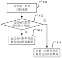
参见图11,一种触发单元的组合方法包括步骤S11至S14。在步骤S11中选择第一时钟门控电路。在步骤S12中进一步判断选择的边沿触发器的类型是上升沿还是下降沿。Referring to FIG. 11 , a combination method of trigger units includes steps S11 to S14. In step S11, the first clock gating circuit is selected. In step S12, it is further determined whether the type of the selected edge trigger is a rising edge or a falling edge.
如果边沿触发器为上升沿触发器,则执行步骤S13。在步骤S13中,第一时钟门控电路在时钟控制信号EN从有效状态翻转至无效状态的时钟周期产生的第二时钟信号CK提供的上升沿作为边沿触发器的触发边沿,即,在时钟控制信号CK翻转的当前时钟周期的触发边沿,边沿触发器可以传输数据。If the edge trigger is a rising edge trigger, execute step S13. In step S13, the rising edge provided by the second clock signal CK generated by the first clock gating circuit during the clock period when the clock control signal EN flips from the active state to the inactive state is used as the triggering edge of the edge trigger, that is, in the clock control The trigger edge of the current clock cycle when the signal CK flips, and the edge trigger can transmit data.
如果边沿触发器为下降沿触发器,则执行步骤S14。在步骤S14中,第一时钟门控电路在时钟控制信号EN从有效状态翻转至无效状态的时钟周期的前一时钟周期产生的第二时钟信号CK提供的下降沿作为边沿触发器的触发边沿,即,在时钟控制信号CK翻转的时钟周期的前一时钟周期的触发边沿,边沿触发器可以传输数据。If the edge trigger is a falling edge trigger, step S14 is executed. In step S14, the falling edge provided by the second clock signal CK generated by the first clock gating circuit in the clock cycle preceding the clock cycle in which the clock control signal EN flips from the active state to the inactive state is used as the triggering edge of the edge trigger, That is, the edge trigger can transmit data at the trigger edge of the clock cycle preceding the clock cycle in which the clock control signal CK is inverted.
图12示出在图10所示的触发单元设计方法中时钟门控电路和边沿触发器的一种组合方法。FIG. 12 shows a combination method of a clock gating circuit and an edge trigger in the trigger unit design method shown in FIG. 10 .
以如图6所示的第一时钟门控电路为例进行说明。第一时钟门控电路在时钟控制信号EN从有效状态翻转至无效状态的时钟周期,时钟门控电路的时钟信号CK屏蔽时钟信号CLK但提供时钟信号CK的上升沿。The first clock gating circuit as shown in FIG. 6 is taken as an example for description. The clock gating circuit of the first clock gating circuit shields the clock signal CLK but provides a rising edge of the clock signal CK during the clock cycle when the clock control signal EN turns from an active state to an inactive state.
根据边沿触发器120的触发边沿,边沿触发器120的类型可以分为上升沿触发器和下降沿触发器。在选择时钟门控电路的类型之后,将边沿触发器和时钟门控电路组合成触发单元。第一时钟门控电路和第二时钟门控电路,可以直接产生第二时钟信号,对第二时钟信号进行反相以产生第三时钟信号,向任意类型的边沿触发器提供触发边沿。According to the triggering edge of the edge trigger 120 , the types of the edge trigger 120 can be divided into rising edge triggers and falling edge triggers. After selecting the type of clock gating circuit, combine the edge trigger and clock gating circuit into a trigger unit. The first clock gating circuit and the second clock gating circuit can directly generate the second clock signal, invert the second clock signal to generate the third clock signal, and provide a trigger edge for any type of edge trigger.
在选择的时钟门控电路和边沿触发器组合成触发单元时,可以采用与边沿触发器的类型相对应的触发方式提供触发边沿。When the selected clock gating circuit and edge trigger are combined into a trigger unit, a trigger mode corresponding to the type of edge trigger can be used to provide a trigger edge.
参见图12,另一种触发单元的组合方法包括步骤S21至S24。在步骤S21中选择第一时钟门控电路。在步骤S22中进一步判断选择的边沿触发器的类型是上升沿还是下降沿。Referring to FIG. 12 , another combination method of trigger units includes steps S21 to S24. In step S21, the first clock gating circuit is selected. In step S22, it is further determined whether the type of the selected edge trigger is a rising edge or a falling edge.
如果边沿触发器为上升沿触发器,则执行步骤S23。在步骤S23中,第一时钟门控电路在时钟控制信号EN从有效状态翻转至无效状态的时钟周期产生的第二时钟信号CK提供的上升沿作为边沿触发器的触发边沿,即,在时钟控制信号CK翻转的当前时钟周期的触发边沿,边沿触发器可以传输数据。If the edge trigger is a rising edge trigger, step S23 is executed. In step S23, the rising edge provided by the second clock signal CK generated by the first clock gating circuit during the clock period when the clock control signal EN flips from the active state to the inactive state is used as the triggering edge of the edge trigger, that is, in the clock control The trigger edge of the current clock cycle when the signal CK flips, and the edge trigger can transmit data.
如果边沿触发器为下降沿触发器,则执行步骤S24。在步骤S24中,对第二时钟信号进行反相以产生第三时钟信号,第一时钟门控电路在时钟控制信号EN从有效状态翻转至无效状态的时钟周期产生第二时钟信号CK,将第二时钟信号CK的反相信号提供的下降沿作为边沿触发器的触发边沿,即,在时钟控制信号CK翻转的当前时钟周期的触发边沿,边沿触发器可以传输数据。If the edge trigger is a falling edge trigger, execute step S24. In step S24, inverting the second clock signal to generate a third clock signal, the first clock gating circuit generates the second clock signal CK in the clock period when the clock control signal EN is flipped from an active state to an inactive state, and converts the second clock signal to an invalid state. The falling edge provided by the inverted signal of the two clock signals CK serves as the triggering edge of the edge trigger, that is, the edge trigger can transmit data at the triggering edge of the current clock period when the clock control signal CK is inverted.
在上述的触发单元的设计方法中描述了根据时钟控制信号的信号延迟选择边沿触发器的三种时钟门控电路之一。可以理解,在数字电路的设计中,可以将时钟控制信号控制为仅在时钟信号CLK的第一电平阶段翻转,因此,可以根据边沿触发器的类型从两种时钟门控电路中选择边沿触发器的时钟门控电路。In the design method of the trigger unit described above, one of the three kinds of clock gating circuits for selecting the edge trigger is described according to the signal delay of the clock control signal. It can be understood that in the design of digital circuits, the clock control signal can be controlled to be inverted only at the first level stage of the clock signal CLK, therefore, edge triggering can be selected from two types of clock gating circuits according to the type of edge triggering tor clock gating circuit.
在上述的触发单元中,以在时钟信号的上升沿触发和下降沿触发的触发器为例进行说明,触发单元内的边沿触发器仅示例了一种结构。然而,本发明不限于此。可以理解,其他的边沿触发器,例如带复位功能的边沿触发器,也可应用本发明进行技术改善。In the above trigger unit, the flip-flop triggered on the rising edge and the falling edge of the clock signal is taken as an example for illustration, and the edge trigger in the trigger unit is only an example of a structure. However, the present invention is not limited thereto. It can be understood that other edge triggers, such as edge triggers with a reset function, can also be technically improved by applying the present invention.
应当说明的是,在本文中,诸如第一和第二等之类的关系术语仅仅用来将一个实体或者操作与另一个实体或操作区分开来,而不一定要求或者暗示这些实体或操作之间存在任何这种实际的关系或者顺序。而且,术语“包括”、“包含”或者其任何其他变体意在涵盖非排他性的包含,从而使得包括一系列要素的过程、方法、物品或者设备不仅包括那些要素,而且还包括没有明确列出的其他要素,或者是还包括为这种过程、方法、物品或者设备所固有的要素。在没有更多限制的情况下,由语句“包括一个……”限定的要素,并不排除在包括所述要素的过程、方法、物品或者设备中还存在另外的相同要素。It should be noted that in this article, relational terms such as first and second etc. are only used to distinguish one entity or operation from another entity or operation, and do not necessarily require or imply that there is a relationship between these entities or operations. There is no such actual relationship or order between them. Furthermore, the term "comprises", "comprises" or any other variation thereof is intended to cover a non-exclusive inclusion such that a process, method, article, or apparatus comprising a set of elements includes not only those elements, but also includes elements not expressly listed. other elements of or also include elements inherent in such a process, method, article, or apparatus. Without further limitations, an element defined by the phrase "comprising a ..." does not exclude the presence of additional identical elements in the process, method, article or apparatus comprising said element.
依照本发明的实施例如上文所述,这些实施例并没有详尽叙述所有的细节,也不限制该发明仅为所述的具体实施例。显然,根据以上描述,可作很多的修改和变化。本说明书选取并具体描述这些实施例,是为了更好地解释本发明的原理和实际应用,从而使所属技术领域技术人员能很好地利用本发明以及在本发明基础上的修改使用。本发明仅受权利要求书及其全部范围和等效物的限制。Embodiments according to the present invention are described above, and these embodiments do not describe all details in detail, nor do they limit the invention to only the specific embodiments described. Obviously many modifications and variations are possible in light of the above description. This description selects and specifically describes these embodiments in order to better explain the principles and practical applications of the present invention, so that those skilled in the art can make good use of the present invention and its modification on the basis of the present invention. The invention is to be limited only by the claims, along with their full scope and equivalents.
Claims (16)
Priority Applications (5)
| Application Number | Priority Date | Filing Date | Title |
|---|---|---|---|
| CN202210107336.2A CN114417759B (en) | 2022-01-28 | 2022-01-28 | Design method of trigger unit |
| PCT/CN2023/080582 WO2023143631A1 (en) | 2022-01-28 | 2023-03-09 | Trigger unit design method |
| JP2024544831A JP7834874B2 (en) | 2022-01-28 | 2023-03-09 | Trigger unit design method |
| EP23746507.5A EP4485270A4 (en) | 2022-01-28 | 2023-03-09 | TRIGGER UNIT DESIGN PROCEDURE |
| US18/832,270 US20250165687A1 (en) | 2022-01-28 | 2023-03-09 | Design method for flip-flop unit |
Applications Claiming Priority (1)
| Application Number | Priority Date | Filing Date | Title |
|---|---|---|---|
| CN202210107336.2A CN114417759B (en) | 2022-01-28 | 2022-01-28 | Design method of trigger unit |
Publications (2)
| Publication Number | Publication Date |
|---|---|
| CN114417759A CN114417759A (en) | 2022-04-29 |
| CN114417759B true CN114417759B (en) | 2022-12-20 |
Family
ID=81279048
Family Applications (1)
| Application Number | Title | Priority Date | Filing Date |
|---|---|---|---|
| CN202210107336.2A Active CN114417759B (en) | 2022-01-28 | 2022-01-28 | Design method of trigger unit |
Country Status (5)
| Country | Link |
|---|---|
| US (1) | US20250165687A1 (en) |
| EP (1) | EP4485270A4 (en) |
| JP (1) | JP7834874B2 (en) |
| CN (1) | CN114417759B (en) |
| WO (1) | WO2023143631A1 (en) |
Families Citing this family (2)
| Publication number | Priority date | Publication date | Assignee | Title |
|---|---|---|---|---|
| CN114417759B (en) * | 2022-01-28 | 2022-12-20 | 杭州士兰微电子股份有限公司 | Design method of trigger unit |
| CN115225084A (en) * | 2022-08-18 | 2022-10-21 | 本征信息技术(苏州)有限公司 | A phase detection circuit and its operation method |
Family Cites Families (16)
| Publication number | Priority date | Publication date | Assignee | Title |
|---|---|---|---|---|
| JP3357813B2 (en) * | 1997-04-01 | 2002-12-16 | 株式会社東芝 | Gated clock design support method, gated clock design support device, and computer-readable recording medium storing gated clock design support program |
| JP3179363B2 (en) * | 1997-04-18 | 2001-06-25 | 日本電気株式会社 | Circuit design method and storage medium |
| US6457167B1 (en) * | 1998-03-31 | 2002-09-24 | Kabushiki Kaisha Toshiba | Gated clock design supporting method, gated clock design supporting apparatus, and computer readable memory storing gated clock design supporting program |
| US6718523B2 (en) * | 2001-07-05 | 2004-04-06 | International Business Machines Corporation | Reduced pessimism clock gating tests for a timing analysis tool |
| US7076748B2 (en) | 2003-08-01 | 2006-07-11 | Atrenta Inc. | Identification and implementation of clock gating in the design of integrated circuits |
| CN101078944B (en) * | 2007-05-11 | 2010-05-26 | 东南大学 | Clock switching circuit |
| GB2466300B (en) * | 2008-12-19 | 2013-05-15 | Advanced Risc Mach Ltd | Control of clock gating |
| SG188112A1 (en) * | 2009-10-30 | 2013-03-28 | Semiconductor Energy Lab | Logic circuit and semiconductor device |
| JP2011164988A (en) | 2010-02-10 | 2011-08-25 | Fujitsu Semiconductor Ltd | Design device |
| CN102857198B (en) * | 2012-08-30 | 2015-09-30 | 锐迪科科技有限公司 | Clock gating circuit for dual edge triggers |
| US9053257B2 (en) * | 2012-11-05 | 2015-06-09 | Advanced Micro Devices, Inc. | Voltage-aware signal path synchronization |
| US9317639B1 (en) * | 2014-10-27 | 2016-04-19 | Freescale Semiconductor, Inc. | System for reducing power consumption of integrated circuit |
| CN104852712A (en) * | 2015-05-19 | 2015-08-19 | 中国电子科技集团公司第四十七研究所 | Low-power-consumption gated clock circuit structure based on data variation |
| KR102688567B1 (en) * | 2019-10-30 | 2024-07-25 | 삼성전자주식회사 | Clock gating cell with low power and integrated circuit including the same |
| CN114417758B (en) | 2022-01-28 | 2023-06-20 | 杭州士兰微电子股份有限公司 | Trigger unit for clock gating based on data compare |
| CN114417759B (en) * | 2022-01-28 | 2022-12-20 | 杭州士兰微电子股份有限公司 | Design method of trigger unit |
-
2022
- 2022-01-28 CN CN202210107336.2A patent/CN114417759B/en active Active
-
2023
- 2023-03-09 US US18/832,270 patent/US20250165687A1/en active Pending
- 2023-03-09 EP EP23746507.5A patent/EP4485270A4/en active Pending
- 2023-03-09 JP JP2024544831A patent/JP7834874B2/en active Active
- 2023-03-09 WO PCT/CN2023/080582 patent/WO2023143631A1/en not_active Ceased
Non-Patent Citations (3)
| Title |
|---|
| 一种新型低功耗触发器的设计;刘欢 等;《沈阳化工学院学报》;20070915;全文 * |
| 基于门控时钟技术的低功耗三值 D 型触发器设计;叶锡恩 等;《电路与系统学报》;20060630;全文 * |
| 基于门控时钟的低功耗时序电路设计新方法;徐扬 等;《浙江大学学报(工学版)》;20100915;全文 * |
Also Published As
| Publication number | Publication date |
|---|---|
| WO2023143631A1 (en) | 2023-08-03 |
| JP2025502539A (en) | 2025-01-24 |
| JP7834874B2 (en) | 2026-03-24 |
| EP4485270A1 (en) | 2025-01-01 |
| US20250165687A1 (en) | 2025-05-22 |
| CN114417759A (en) | 2022-04-29 |
| EP4485270A4 (en) | 2026-01-14 |
Similar Documents
| Publication | Publication Date | Title |
|---|---|---|
| CN114417758B (en) | Trigger unit for clock gating based on data compare | |
| CN114417760B (en) | Trigger unit containing clock gating circuit | |
| US8786344B2 (en) | Low-power dual-edge-triggered storage cell with scan test support and clock gating circuit therefor | |
| US6864735B2 (en) | Circuit and method for regenerating reset and clock signals and high-speed digital system incorporating the same | |
| CN114417759B (en) | Design method of trigger unit | |
| KR100432923B1 (en) | Register capable of corresponding to wide frequency band and signal generating method using the same | |
| KR100612417B1 (en) | Pulse-based high speed low power gated flop flop circuit | |
| US9317639B1 (en) | System for reducing power consumption of integrated circuit | |
| US6192004B1 (en) | Semiconductor integrated circuit | |
| JP3930513B2 (en) | Flip-flop circuit having a majority logic circuit | |
| TWI821198B (en) | Integrated circuit, non-transitory computer readable medium and computing system | |
| US10901454B2 (en) | Clock buffering to reduce memory hold time | |
| JP3629019B2 (en) | Semiconductor integrated circuit | |
| Al-bayati et al. | Design of a C-element based clock domain crossing interface | |
| JP2006300669A (en) | Scan flip-flop and semiconductor integrated circuit using the same | |
| JPH06174804A (en) | Semiconductor integrated circuit | |
| JP2019186854A (en) | Semiconductor integrated circuit | |
| JPH1124796A (en) | Power-on reset circuit | |
| JPH06282359A (en) | Configuration control circuit | |
| JPH07201169A (en) | Semiconductor memory |
Legal Events
| Date | Code | Title | Description |
|---|---|---|---|
| PB01 | Publication | ||
| PB01 | Publication | ||
| SE01 | Entry into force of request for substantive examination | ||
| SE01 | Entry into force of request for substantive examination | ||
| GR01 | Patent grant | ||
| GR01 | Patent grant | ||
| EE01 | Entry into force of recordation of patent licensing contract | ||
| EE01 | Entry into force of recordation of patent licensing contract |
Application publication date: 20220429 Assignee: Hangzhou Pailixin Technology Co.,Ltd. Assignor: HANGZHOU SILAN MICROELECTRONICS Co.,Ltd. Contract record no.: X2025980020100 Denomination of invention: Design methods for trigger units Granted publication date: 20221220 License type: Exclusive License Record date: 20250829 |