CN114324344A - Non-lambert surface inspection system for line scanning - Google Patents

Non-lambert surface inspection system for line scanning Download PDF

Info

Publication number
CN114324344A
CN114324344A CN202111137167.9A CN202111137167A CN114324344A CN 114324344 A CN114324344 A CN 114324344A CN 202111137167 A CN202111137167 A CN 202111137167A CN 114324344 A CN114324344 A CN 114324344A
Authority
CN
China
Prior art keywords
image
illumination
module
block
illumination image
Prior art date
Legal status (The legal status is an assumption and is not a legal conclusion. Google has not performed a legal analysis and makes no representation as to the accuracy of the status listed.)
Pending
Application number
CN202111137167.9A
Other languages
Chinese (zh)
Inventor
权仁洙
尹汝鹤
全雄俊
朴水烈
Current Assignee (The listed assignees may be inaccurate. Google has not performed a legal analysis and makes no representation or warranty as to the accuracy of the list.)
Honeycomb Vision Co ltd
Original Assignee
Honeycomb Vision Co ltd
Priority date (The priority date is an assumption and is not a legal conclusion. Google has not performed a legal analysis and makes no representation as to the accuracy of the date listed.)
Filing date
Publication date
Application filed by Honeycomb Vision Co ltd filed Critical Honeycomb Vision Co ltd
Publication of CN114324344A publication Critical patent/CN114324344A/en
Pending legal-status Critical Current

Links

Images

Classifications

    • GPHYSICS
    • G06COMPUTING OR CALCULATING; COUNTING
    • G06TIMAGE DATA PROCESSING OR GENERATION, IN GENERAL
    • G06T7/00Image analysis
    • G06T7/0002Inspection of images, e.g. flaw detection
    • G06T7/0004Industrial image inspection
    • G06T7/0006Industrial image inspection using a design-rule based approach
    • GPHYSICS
    • G01MEASURING; TESTING
    • G01NINVESTIGATING OR ANALYSING MATERIALS BY DETERMINING THEIR CHEMICAL OR PHYSICAL PROPERTIES
    • G01N21/00Investigating or analysing materials by the use of optical means, i.e. using sub-millimetre waves, infrared, visible or ultraviolet light
    • G01N21/84Systems specially adapted for particular applications
    • G01N21/88Investigating the presence of flaws or contamination
    • G01N21/8806Specially adapted optical and illumination features
    • GPHYSICS
    • G01MEASURING; TESTING
    • G01NINVESTIGATING OR ANALYSING MATERIALS BY DETERMINING THEIR CHEMICAL OR PHYSICAL PROPERTIES
    • G01N21/00Investigating or analysing materials by the use of optical means, i.e. using sub-millimetre waves, infrared, visible or ultraviolet light
    • G01N21/84Systems specially adapted for particular applications
    • G01N21/88Investigating the presence of flaws or contamination
    • G01N21/95Investigating the presence of flaws or contamination characterised by the material or shape of the object to be examined
    • G01N21/9515Objects of complex shape, e.g. examined with use of a surface follower device
    • GPHYSICS
    • G06COMPUTING OR CALCULATING; COUNTING
    • G06TIMAGE DATA PROCESSING OR GENERATION, IN GENERAL
    • G06T5/00Image enhancement or restoration
    • G06T5/40Image enhancement or restoration using histogram techniques
    • GPHYSICS
    • G06COMPUTING OR CALCULATING; COUNTING
    • G06TIMAGE DATA PROCESSING OR GENERATION, IN GENERAL
    • G06T7/00Image analysis
    • G06T7/0002Inspection of images, e.g. flaw detection
    • G06T7/0004Industrial image inspection
    • GPHYSICS
    • G06COMPUTING OR CALCULATING; COUNTING
    • G06TIMAGE DATA PROCESSING OR GENERATION, IN GENERAL
    • G06T7/00Image analysis
    • G06T7/30Determination of transform parameters for the alignment of images, i.e. image registration
    • G06T7/33Determination of transform parameters for the alignment of images, i.e. image registration using feature-based methods
    • GPHYSICS
    • G06COMPUTING OR CALCULATING; COUNTING
    • G06TIMAGE DATA PROCESSING OR GENERATION, IN GENERAL
    • G06T7/00Image analysis
    • G06T7/30Determination of transform parameters for the alignment of images, i.e. image registration
    • G06T7/35Determination of transform parameters for the alignment of images, i.e. image registration using statistical methods
    • GPHYSICS
    • G06COMPUTING OR CALCULATING; COUNTING
    • G06TIMAGE DATA PROCESSING OR GENERATION, IN GENERAL
    • G06T7/00Image analysis
    • G06T7/40Analysis of texture
    • G06T7/41Analysis of texture based on statistical description of texture
    • G06T7/44Analysis of texture based on statistical description of texture using image operators, e.g. filters, edge density metrics or local histograms
    • GPHYSICS
    • G06COMPUTING OR CALCULATING; COUNTING
    • G06TIMAGE DATA PROCESSING OR GENERATION, IN GENERAL
    • G06T7/00Image analysis
    • G06T7/50Depth or shape recovery
    • G06T7/55Depth or shape recovery from multiple images
    • G06T7/586Depth or shape recovery from multiple images from multiple light sources, e.g. photometric stereo
    • GPHYSICS
    • G06COMPUTING OR CALCULATING; COUNTING
    • G06TIMAGE DATA PROCESSING OR GENERATION, IN GENERAL
    • G06T7/00Image analysis
    • G06T7/60Analysis of geometric attributes
    • GPHYSICS
    • G06COMPUTING OR CALCULATING; COUNTING
    • G06VIMAGE OR VIDEO RECOGNITION OR UNDERSTANDING
    • G06V30/00Character recognition; Recognising digital ink; Document-oriented image-based pattern recognition
    • G06V30/10Character recognition
    • G06V30/19Recognition using electronic means
    • G06V30/19007Matching; Proximity measures
    • G06V30/19073Comparing statistics of pixel or of feature values, e.g. histogram matching
    • GPHYSICS
    • G01MEASURING; TESTING
    • G01NINVESTIGATING OR ANALYSING MATERIALS BY DETERMINING THEIR CHEMICAL OR PHYSICAL PROPERTIES
    • G01N21/00Investigating or analysing materials by the use of optical means, i.e. using sub-millimetre waves, infrared, visible or ultraviolet light
    • G01N21/84Systems specially adapted for particular applications
    • G01N21/88Investigating the presence of flaws or contamination
    • G01N21/8806Specially adapted optical and illumination features
    • G01N2021/8812Diffuse illumination, e.g. "sky"
    • G01N2021/8816Diffuse illumination, e.g. "sky" by using multiple sources, e.g. LEDs
    • GPHYSICS
    • G01MEASURING; TESTING
    • G01NINVESTIGATING OR ANALYSING MATERIALS BY DETERMINING THEIR CHEMICAL OR PHYSICAL PROPERTIES
    • G01N21/00Investigating or analysing materials by the use of optical means, i.e. using sub-millimetre waves, infrared, visible or ultraviolet light
    • G01N21/84Systems specially adapted for particular applications
    • G01N21/88Investigating the presence of flaws or contamination
    • G01N21/8851Scan or image signal processing specially adapted therefor, e.g. for scan signal adjustment, for detecting different kinds of defects, for compensating for structures, markings, edges
    • G01N2021/8854Grading and classifying of flaws
    • G01N2021/8867Grading and classifying of flaws using sequentially two or more inspection runs, e.g. coarse and fine, or detecting then analysing
    • G01N2021/887Grading and classifying of flaws using sequentially two or more inspection runs, e.g. coarse and fine, or detecting then analysing the measurements made in two or more directions, angles, positions
    • GPHYSICS
    • G01MEASURING; TESTING
    • G01NINVESTIGATING OR ANALYSING MATERIALS BY DETERMINING THEIR CHEMICAL OR PHYSICAL PROPERTIES
    • G01N21/00Investigating or analysing materials by the use of optical means, i.e. using sub-millimetre waves, infrared, visible or ultraviolet light
    • G01N21/84Systems specially adapted for particular applications
    • G01N21/88Investigating the presence of flaws or contamination
    • G01N21/8851Scan or image signal processing specially adapted therefor, e.g. for scan signal adjustment, for detecting different kinds of defects, for compensating for structures, markings, edges
    • G01N2021/8887Scan or image signal processing specially adapted therefor, e.g. for scan signal adjustment, for detecting different kinds of defects, for compensating for structures, markings, edges based on image processing techniques
    • GPHYSICS
    • G06COMPUTING OR CALCULATING; COUNTING
    • G06TIMAGE DATA PROCESSING OR GENERATION, IN GENERAL
    • G06T2207/00Indexing scheme for image analysis or image enhancement
    • G06T2207/10Image acquisition modality
    • G06T2207/10141Special mode during image acquisition
    • G06T2207/10152Varying illumination
    • GPHYSICS
    • G06COMPUTING OR CALCULATING; COUNTING
    • G06TIMAGE DATA PROCESSING OR GENERATION, IN GENERAL
    • G06T2207/00Indexing scheme for image analysis or image enhancement
    • G06T2207/20Special algorithmic details
    • G06T2207/20021Dividing image into blocks, subimages or windows
    • GPHYSICS
    • G06COMPUTING OR CALCULATING; COUNTING
    • G06TIMAGE DATA PROCESSING OR GENERATION, IN GENERAL
    • G06T2207/00Indexing scheme for image analysis or image enhancement
    • G06T2207/30Subject of image; Context of image processing
    • G06T2207/30108Industrial image inspection
    • G06T2207/30164Workpiece; Machine component

Landscapes

  • Engineering & Computer Science (AREA)
  • Physics & Mathematics (AREA)
  • General Physics & Mathematics (AREA)
  • Theoretical Computer Science (AREA)
  • Computer Vision & Pattern Recognition (AREA)
  • Life Sciences & Earth Sciences (AREA)
  • Probability & Statistics with Applications (AREA)
  • Pathology (AREA)
  • Immunology (AREA)
  • Health & Medical Sciences (AREA)
  • Chemical & Material Sciences (AREA)
  • Analytical Chemistry (AREA)
  • Biochemistry (AREA)
  • General Health & Medical Sciences (AREA)
  • Quality & Reliability (AREA)
  • Bioinformatics & Cheminformatics (AREA)
  • Bioinformatics & Computational Biology (AREA)
  • Evolutionary Biology (AREA)
  • Geometry (AREA)
  • Multimedia (AREA)
  • Investigating Materials By The Use Of Optical Means Adapted For Particular Applications (AREA)

Abstract

本发明涉及行扫描用非郎伯表面检查系统,包括:表面检查部,在一侧面以及另一侧面中的至少一个上形成曲线形的搁置孔,包括在上端形成拍摄孔的框架模块以及通过在搁置孔中安装多个而向放置在底面上的被检查物体沿着斜线照射光线的第一照明模块以及第二照明模块;摄像头部,位于拍摄孔的上方,通过贯通拍摄孔并对位于底面上的被检查物体进行拍摄而生成包括第一照明图像以及第二照明图像在内的整体合成图像;以及,控制器部,用于对摄像头部的工作进行控制,通过选择性地驱动第一照明模块以及第二照明模块而从通过摄像头部拍摄到的整体接收图像提取出第一照明图像以及第二照明图像并利用预先设定的公式加工之后进行合成而生成控制器部。

Figure 202111137167

The present invention relates to a non-Lambertian surface inspection system for line scanning, comprising: a surface inspection part, a curvilinear resting hole formed on at least one of one side surface and the other side surface, a frame module forming a shooting hole at the upper end, and a A plurality of first lighting modules and second lighting modules are installed in the resting hole to irradiate light to the inspected object placed on the bottom surface along an oblique line; the camera head, located above the shooting hole, passes through the shooting hole and is located on the bottom surface. The object to be inspected on the camera is photographed to generate an overall composite image including the first illumination image and the second illumination image; and the controller unit is used to control the operation of the camera head by selectively driving the first illumination The module and the second illumination module extract the first illumination image and the second illumination image from the overall received image captured by the camera unit, process the first illumination image and the second illumination image using a preset formula, and synthesize them to generate the controller unit.

Figure 202111137167

Description

Non-lambert surface inspection system for line scanning
Technical Field
The invention relates to the technical field of inspecting the surface of a product by utilizing a camera for line scanning.
Background
Industries such as electric vehicles, hybrid vehicles, and the like, including portable Information Technology (IT) equipment industries such as smart phones, tablet computers, and notebook computers, are rapidly developing. The industries as described above are also leading the development of a variety of subsidiary industries. As an example, along with the increase in the types of smartphones and the reduction in the usage periods of smartphones, the system-related industry that can quickly and accurately check a wide variety of different types of smartphones is growing rapidly.
As a result, the market for appearance defect detection systems associated with smartphone glazings is also becoming increasingly large.
In the past, when inspecting defects on a screen glass of a smartphone, a method of inspecting the shape and surface of an object to be illuminated by a simple illumination method using an Area Scan Camera (Area Scan Camera) and a Line Scan Camera (Line Scan Camera) has been used.
The above-described contour and surface inspection system can only inspect limited types of bad and limited-form models due to its simple structure and low cost, but is still widely used because there is no appropriate alternative at present.
Since the conventional surface inspection system cannot adjust the illumination direction and the light amount according to the model of the different curved surface forms, there is a problem that the inspection cannot be performed or the defect appearing on the light intended to the specific direction cannot be detected because of a glare (glare) phenomenon, that is, a phenomenon that the surface cannot be inspected because of strong white reflection.
Prior art documents
Patent document
(patent document 1) Korean registered patent No. 10-0824808 (publication date: 2008.04.24)
Disclosure of Invention
The invention aims to solve the problem that the surface state of an object to be inspected can not be accurately inspected due to the glare phenomenon when the surface of the object to be inspected is inspected.
The technical subject of the present invention is not limited to the subject mentioned in the above, and other technical subjects not mentioned will be further clearly understood by the relevant practitioner from the following description.
In order to achieve the technical object, a non-lambert line scanning surface inspection system according to the present invention includes: a surface inspection part which forms a curved resting hole on at least one of one side surface and the other side surface, and comprises a frame module forming a shooting hole at the upper end, and a first illumination module and a second illumination module which are arranged in the resting holes and irradiate light rays along an oblique line to an inspected object placed on the bottom surface;
an imaging head unit which is positioned above the imaging hole and which generates an overall composite image including a first illumination image and a second illumination image by imaging the object to be inspected positioned on the bottom surface through the imaging hole; and the number of the first and second groups,
a controller section for controlling an operation of the camera head section, and receiving the first illumination image and the second illumination image captured by the camera head section by selectively driving the first illumination module and the second illumination module to operate;
a controller part for controlling the operation of the display device,
the first lighting module is turned on and then turned off within a set time,
the second lighting module is turned on while the first lighting module is turned off,
receiving a first illumination image photographed by a camera head when a first illumination module is turned on,
receiving a second illumination image captured by the camera head when the second illumination module is turned on,
a controller section including:
an illumination image receiving module for receiving the first illumination image and the second illumination image captured by the camera head in a region of a set Row (Row) or Column (Column);
an alignment module for aligning the partial images of the rows (Row) or columns (Column) of the first illumination image and the partial images of the rows (Row) or columns (Column) of the second illumination image;
a histogram module for dividing the first illumination image and the second illumination image into a plurality of blocks and extracting a reflectance value of each block after assigning a position number to each block;
a removal module which deletes a block having a reflectance value larger than a reference reflectance value by comparing the reference reflectance value set in advance with a reflectance value measured from the block; and the number of the first and second groups,
a block correction image module which receives a block at the same position as the block deleted from the first illumination image from the second illumination image after deleting the block having a reflectance larger than the reference reflectance from the first illumination image and generates a first block correction image by mapping to the first illumination image,
after deleting a block having a reflectance value larger than the reference reflectance value from the second illumination image, receiving a block at the same position as the block deleted from the second illumination image from the first illumination image and generating a second block correction image by mapping to the second illumination image;
the controller portion further includes:
a composite image generation module which generates a composite image by calculating the first block corrected image and the second block corrected image according to a predetermined formula and then synthesizing the calculated images;
a composite image generating module for generating a composite image,
processing the composite image into a reflectivity image in a set area of the composite image,
or calculating the variation of the surface height of the inspected object along the X-axis direction in the composite image and processing the variation into an X-axis partial differential image,
or a Y-axis partial differential image processed to calculate the amount of change in the surface height of the inspected object in the Y-axis direction in the composite image,
or 2 partial differential images obtained by calculating the amount of change in the surface height of the object to be inspected from the X-axis partial differential image and the Y-axis partial differential image in the X-axis direction and the Y-axis direction.
The frame module is used for supporting the frame module,
may be formed in a shape contained in a hemisphere.
The frame module may further include:
and a reflection plate installed on the upper side surface.
The frame module, characterized by, including: a light-transmitting plate installed in the photographing hole and having a dot pattern formed on an upper side surface thereof for reflecting light to a lower direction; and auxiliary lighting modules, which are installed on the side of the light-transmitting plate to irradiate light to the inside of the light-transmitting plate; the auxiliary lighting module is characterized in that the brightness thereof is adjusted by the controller 20.
Drawings
FIG. 1 is a state diagram of a non-Lambertian surface inspection system for line scanning, to which an embodiment of the present invention is applied.
Fig. 2 is a schematic diagram illustrating a plurality of block correction images actually acquired by a non-lambert surface inspection system for line scanning according to an embodiment of the present invention.
FIG. 3 is a block diagram of a non-Lambertian surface inspection system for line scanning, to which an embodiment of the invention is applicable.
Fig. 4 is an oblique view of the surface inspection portion in fig. 1.
Fig. 5 is a schematic view illustrating a rotation state of the lighting module mounted on the frame module illustrated in fig. 4 and a state in which light is diagonally output from the first lighting module and the second lighting module.
Fig. 6 is a schematic view illustrating a surface inspection part in a state where a reflection plate is mounted on the frame module illustrated in fig. 4.
Fig. 7 is a schematic view schematically illustrating a plurality of lighting modules mounted on the frame module illustrated in fig. 4.
FIG. 8 is a sequence diagram relating to the operation of a non-Lambertian surface inspection system for line scanning, to which an embodiment of the present invention is applied.
Fig. 9 to 13 are schematic diagrams illustrating the operation of the line-scanning non-lambert surface inspection system and images displayed during the operation thereof to which an embodiment of the present invention is applied.
Fig. 14 is a schematic diagram illustrating a captured image and a plurality of block corrected images.
Fig. 15 is a perspective view illustrating a form in which the light-transmitting plate is attached to the frame module.
Fig. 16 is a perspective view illustrating a state in which the light-transmitting plate and the reflecting plate are attached to the frame module.
Fig. 17 is a front view and a side view illustrating a form in which scattered light is emitted through the transparent plate.
Fig. 18 is a plan view illustrating the light-transmitting plate.
Fig. 19 is an explanatory diagram illustrating an image difference (left: no scattered light illumination, right: scattered light illumination) with respect to whether scattered light illumination is applied or not.
Fig. 20 is an illustrative view illustrating a process of detecting a scratch and a stab mark.
FIG. 21 is a graph relating to whether scattered light is present or not (left: severe noise, right: noise removed).
FIG. 22 is a histogram of the surface histogram with respect to the presence or absence of scattered light (left: higher deviation due to smoothing and right: lower deviation due to lower smoothing).
[ notation ] to show
1: non-lambert surface inspection system for line scanning
10: surface inspection part
110: frame module
111: placing hole
112: shooting hole
113: reflecting plate
114: light-transmitting plate
121: first lighting module
122: second lighting module
125: auxiliary lighting module
20: camera head
30: controller part
310: illumination image receiving module
320: alignment module
330: histogram module
340: removal module
350: block correction image module
360: composite image generation module
A: inspected object
B: bottom surface
C: receiving images en bloc
D1: first partial image
D2: second partial image
D3: the third partial image
D4: fourth partial image
E1: first illumination image
E2: second illumination image
E3: third illumination image
E4: fourth illumination image
F1, F2, F3, F4: image with divided image blocks and glare part removed
G1: the first block corrects the image
G2: second block correction image
G3: fourth block corrected image
G4: fourth block corrected image
H: composite image
H1: reflectance image
H2: partial differential X-axis image
H3: y-axis partial differential image
H4: partial differential 2-order image
H5: surface vertical vector image
I: light ray
Detailed Description
The drawings illustrated in the present specification and the contents described with reference to the drawings are provided only as exemplary contents to assist those having ordinary knowledge in the technical field of the present invention to more easily understand the present invention. Accordingly, the drawings and detailed description of the invention for practicing the invention are not intended to limit the scope of the claims of the invention. The scope of the claims of the present invention should be defined only by the following claims.
Next, the non-lambertian surface inspection system for line scanning according to the present invention will be described in detail with reference to the drawings of the following embodiments of the present invention. However, in order to more clearly and concisely describe the present invention, a non-lambertian surface inspection system for line scanning will be briefly described with reference to fig. 1 and 2. Further, the constituent elements constituting the non-lambert surface inspection system for line scanning will be described in detail with reference to fig. 3 to 7.
Fig. 1 is a state diagram of a line-scanning non-lambert surface inspection system to which an embodiment of the present invention is applied, and fig. 2 is a schematic diagram illustrating a plurality of composite images applied to a final inspection by the line-scanning non-lambert surface inspection system to which an embodiment of the present invention is applied.
The line scanning non-lambert surface inspection system 1 of the present invention includes a surface inspection unit 10, an image pickup head unit 20, and a controller unit 30 as components, and the controller unit 30 can drive the surface inspection unit 10 and the image pickup head unit 20 to operate. At this time, the plurality of illumination modules included in the surface inspection section 10 output light in a predetermined combination order according to the operation of the controller section 30, and the reflector 113 re-irradiates the object a to be inspected with the light output and scattered from the illumination modules 121 to 12 n.
Further, the controller section 30 of the line-scanning non-lambert surface inspection system 1 drives the camera head section 20 according to the operation of the illumination module to photograph the inspection object a, and acquires the entire reception image C received from the camera head section 20 including surface information under illumination in a plurality of directions.
At this time, the overall received image C can be deformed into a plurality of illumination images E1 to E4 (see fig. 11) by the line images D1 to D4 compounding the respective illumination characteristics contained inside.
At this time, the controller unit 30 of the line-scanning non-lambert surface inspection system 1 may divide the generated illumination images E1 to E4 into regions of rows (Row) or columns (Column) and align the regions of rows (Row) or columns (Column) to generate the individual images F1 to F4, and then may divide the images F1 to F4 (see fig. 13) into blocks, calculate reflectance values of the blocks, and compare the calculated reflectance values with a preset reference reflectance value to remove blocks higher than the reference reflectance value. Further, the block correction image is generated by interpolating the block corresponding to the removed portion with the other effective images.
The block correction images G1-G4 may be formed according to the number of the lighting modules 121-12 n. As an example, in the case of having four lighting modules, the first to fourth area correction images G1 to G4 may be generated.
Next, the line scanning non-lambert surface inspection system 1 may generate the synthesized image H by synthesizing at least 2 of the generated plurality of patch correction images G1 to G4. Specifically, as shown in fig. 2, at least 2 of the first to fourth block corrected images G1 to G4 may be synthesized to be processed into a reflectance image H1, an image H2 partially differentiated in the X direction, an image H3 partially differentiated in the Y direction, a 2-th-order partial differential image H4, and a vertical vector image H5.
Accordingly, the non-lambert surface inspection system 1 for line scanning according to the present invention can solve the problem of the conventional surface inspection system, that is, prevent the occurrence of the glare phenomenon when inspecting the surface of the model having the curved surface form, by using the camera head 20 and the plurality of illumination modules 121 to 124 deflected to different angles, and by using the reflectance and the shadow in different illumination directions.
Further, the line-scanning non-lambert surface inspection system 1 of the present invention can improve the reliability of inspection of an object to be inspected by selecting and combining the images in accordance with the measurement and the inspection object.
With this, the line-scanning non-lambert surface inspection system 1 can accurately detect black stains and black scratches, puncture marks, and other flaws formed on the inspection object a in the industrial field, particularly, in the objects subjected to smoke and carbonization stains such as welding.
Next, the components constituting the non-lambert surface inspection system for line scanning will be described in detail with reference to fig. 3 to 7.
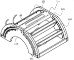
Fig. 3 is a block diagram of a non-lambertian surface inspection system for line scanning according to an embodiment of the present invention, and fig. 4 is an oblique view of the surface inspection part in fig. 1. Fig. 5 is a schematic view illustrating a state in which the lighting module mounted on the frame module illustrated in fig. 4 is rotated and light is diagonally output from the first lighting module and the second lighting module, and fig. 6 is a schematic view illustrating the surface inspection unit in a state in which the reflector is mounted on the frame module illustrated in fig. 4. Further, fig. 7 is a schematic view schematically illustrating a plurality of lighting modules mounted on the frame module illustrated in fig. 4.
The surface inspection unit 10 is a device that irradiates light onto an object a to be inspected at a plurality of different angles in order to image the object a to be inspected with the image pickup head 20. The surface inspection part 10 as described above is formed in a shape included in a hemisphere, and includes a frame module 110 formed with a photographing hole 112 at an upper end, and an illumination module mounted on the frame module 110 and rotated and moved.
As shown in fig. 4, a curved rest hole 111 is formed in at least one of one side surface and the other side surface of the frame module 110, and a plurality of illumination modules for diagonally outputting light to the inspected object a placed on the bottom surface are installed in the rest hole 111.
In this case, the plurality of illumination modules are illumination for a Shadow Metric System (SMS) optimized for Line Scan (Line Scan). In this specification, the first illumination module 121, the second illumination module 122, the third illumination module 123, and the fourth illumination module 124 will be taken as an example in order to more simply and clearly describe the plurality of illumination modules mounted in the surface inspection unit 10. At this time, the first, second, third, and fourth illumination modules 121, 122, 123, and 124 may be illumination for a Shadow-metric System (SMS) optimized for Line Scan (Line Scan). The first to fourth illumination modules 121 to 124 as described above may be selectively rotated in the rest hole 111 as shown in fig. 5 (a), or may output light in a state of being inclined at 45 degrees as shown in fig. 5 (b) and (c).
Further, the surface inspection part 10 may include a reflection plate 113 installed on an upper side of the frame module 110 as shown in fig. 6 so as to be irradiated again onto the inspection object a by reflecting the light outputted and scattered from the plurality of illumination modules. At this time, the first lighting module 121 is installed at the lower end of the placement hole 111 at the left side, and the second lighting module 122 is installed at the upper end of the placement hole 111 at the left side with a certain interval from the first lighting module 121. In addition, a third lighting module 123 is installed at an upper end of the resting hole 111 at the right side, and a fourth lighting module 124 is installed at a lower end of the resting hole 111 at the right side with a certain interval from the third lighting module 123.
As described above, the first to 4 th illumination modules 121 to 124 installed at intervals in the rest hole 111 may be rotated at the installed position and irradiate light toward the inspected object a in various different directions. Further, the light may be irradiated to the inspection object a at a plurality of different positions while moving along the placement hole 111.
The camera head 20 is located above the imaging hole 112 and shoots the inspection object a located on the bottom surface B through the imaging hole 112, thereby receiving the whole image C including the first illumination image E1 and the second illumination image E2.
Specifically, the camera head portion 20 may be attached to the upper side of the shooting hole 112 in such a manner that the lens is positioned to overlap the shooting hole 112. The camera head 20 as described above can shoot the object a to be inspected on the bottom surface through the shooting hole 112, thereby generating an illumination image.
The camera head section 20 as described above operates in accordance with a control signal output from the controller section 30. In particular, the operation of the camera head 20 may be synchronized with the operation of the illumination modules 121 to 12n, so that the camera head operates only when the illumination modules 121 to 12n are turned on and photographs the object a to be inspected.
The camera head 20 as described above may generate the first illumination image E1 to the fourth illumination image E4 when the first illumination module 121, the second illumination module 122, the third illumination module 123, and the fourth illumination module 124 are turned on in combination and in a designated order according to an inspection object. As an example, the camera head 20 captures a first illumination image E1 when the first illumination module 121 is turned on, a second illumination image E2 when the second illumination module 122 is turned on, a third illumination image E3 when the third illumination module 123 is turned on, and a fourth illumination image E4 when the fourth illumination module 124 is turned on.
The controller section 30 is a computer that generates a control signal and receives and processes data. The controller section 30 described above can control the illumination time and the delay time in nanoseconds (nanoseconds) in the cross illumination control by Line Scan (Line Scan). The controller unit 30 includes a separate control board on which a Field Programmable Gate Array (FPGA) chip is mounted because the conventional controller control board using a Microcontroller central processing unit (Microcontroller CPU) is limited.
Therefore, the controller section 30 can immediately reflect problems occurring in the field such as the lighting order, frequency division, and noise removal into the program according to the inspection object. As shown in fig. 3, the controller unit 30 may include an illumination image receiving module 310, an alignment module 320, a histogram module 330, a removal module 340, a patch correction image module 350, a composite image generation module 360, a control signal generation module 370, and the like.
The controller unit 30 as described above may generate a control signal in the control signal generation module 370 and drive the plurality of illumination modules 12 and the camera head unit 20 to operate. As an example, the controller part 30 may turn off after turning on the first lighting module 121 for a certain time, and turn on the second lighting module 122 while turning off the first lighting module 121. Further, the third lighting module 123 may be turned on when the second lighting module 122 is turned off, and the fourth lighting module 124 may be turned on when the third lighting module 123 is turned off.
The controller part 30 is used to turn on and off the first to fourth lighting modules 121 to 124, and may turn on the first to fourth lighting modules 121 to 124. The controller unit 30 may periodically turn on the particular individual illuminations while excluding them or adjusting their brightness according to a preset reference based on the inspection speed efficiency every line scan. As an example, for an a inspected object, the first illumination module 121, the second illumination module 122, and the fourth illumination module 124 may be sequentially turned on and generate a first illumination image, a second illumination image, and a fourth illumination image, and for a B inspected object, the first illumination module 121, the second illumination module 122, and the third illumination module 123 may be sequentially turned on and generate a first illumination image, a second illumination image, and a third illumination image.
Further, the controller section 30 may drive the camera section 20 to generate the first to fourth illumination images and receive the generated respective illumination images. The controller section 30 can generate processed images, that is, a reflectance image H1, an image H2 partially differentiated in the X direction, an image H3 partially differentiated in the Y direction, an image H4 partially differentiated 2 times, and a vertical vector image H5 by processing the illumination image.
Specifically, the controller section 30 may acquire the whole image C including a plurality of image information from the camera section 20 through the illumination image receiving module 310. Further, image divisions D1 to D4 of different illumination groups are selectively extracted from the whole image C and first to fourth illumination images E1 to E4 are generated, and then the respective images are divided in the set Row (Row) or Column (Column) regions.
In addition, the partial images D1 to D4 of the rows (Row) or columns (Column) of the first illumination image E1 and the partial images D1 to D4 of the rows (Row) or columns (Column) of the second illumination image E2 are aligned by the alignment module 320. In addition, the blocks are partitioned into the same size by the histogram module 330 and the reflectivity values of the blocks are extracted after the position numbers are allocated to the blocks. In addition, the removal module 340 deletes a patch having a reflectance value larger than the reference reflectance value by comparing the set reference reflectance value with the reflectance value measured from the patch. In addition, the block correction image module 350 and the removal module 340 interpolate the block corresponding to the removed portion by using the other effective images to generate the first block correction image G1 and the second block correction image G2, respectively.
As an example, when the reflectance value of the first patch HU2 of the second illumination image is greater than the reference reflectance value, the reflectance value of the first patch HU2 is changed to 0. In addition, the average of the reflectance values of the first patch HU1 of the first illumination image and the reflectance values of the first patch HU3 of the third illumination image and the reflectance values of the first patch HU4 of the fourth illumination image is reflected in the first patch HU2 of the second illumination image.
Further, when the luminosity value of the second block HD3 of the third illumination image is larger than the reference luminosity value, the luminosity value of the second block HD2 is changed to 0. Further, the average of the reflectance value of the second section HD2 of the first illumination image, the reflectance value of the second section HD2 of the second illumination image, and the reflectance value of the second section HD4 of the fourth illumination image is reflected into the second section HD3 of the third illumination image.
The first and second block corrected images G1 and G2 are combined by the combined image generation module 360 to generate a combined image H.
In addition to the above features, the controller unit 30 may be configured by a computer to freely adjust the lighting order of the plurality of lighting modules, and may adjust the brightness of each of the lighting modules by a Pulse Width Modulation (PWM) method from the first to fourth lighting modules. Further, since the brightness of illumination at different illumination angles may differ depending on the characteristics of the inspected object, a normalized inspection result can be obtained by managing the illumination value to be irradiated to the inspected object a.
Next, the operation of the non-lambertian surface inspection system for line scanning will be described in detail with reference to fig. 8 to 14.
Fig. 8 is a sequence diagram related to the operation of the non-lambert line scanning surface inspection system according to an embodiment of the present invention, and fig. 9 to 13 are schematic diagrams illustrating the operation and images of the non-lambert line scanning surface inspection system according to an embodiment of the present invention. Fig. 14 is a schematic diagram illustrating a plurality of block correction images.
As shown in fig. 8, the controller unit 30 operates in a series of procedures to generate a reflectance image H1, an image H2 partially differentiated in the X direction, an image H3 partially differentiated in the Y direction, an image H4 partially differentiated 2 times, and a vertical vector image (Norm image), which are processed images.
Specifically, as shown in fig. 9, the controller section 30 sequentially drives the plurality of illumination modules to operate when the object a to be inspected enters the surface inspection section 10, and generates a plurality of illumination images by the camera section 20. At this time, the first to fourth illumination modules 121 to 124 irradiate light to the inspection object a in different directions as shown in fig. 10. The controller part 30 may receive the entire image C according to the operations of the first to fourth illumination modules 121 to 124. Further, the partial images D1 to D4 of a plurality of rows (Row) or columns (Column) may be extracted from the received overall composite image C, and the first illumination image E1 to the fourth illumination image E4 may be generated by aligning the extracted respective partial images.
The controller unit 30 divides the block into a plurality of blocks as shown in fig. 13, extracts a reflectance value from the divided blocks, and compares the reflectance value of the extracted block with a preset reference reflectance value. Among them, the histogram module 330 of the controller part 30 divides the first through fourth illumination images E1 through E4 into blocks F and assigns position numbers to the blocks F, and then extracts reflectance values from the respective blocks. Further, a graph corresponding to the reflectance value may be formed.
In addition, the patches F generated in the histogram module 330 may be pixels, and the reflectance values included in each patch may be extracted within a range of 0 to 255.
Further, 
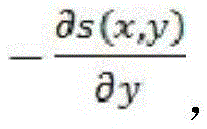
histogram module 330 may extract reflectance values based on the illustrated tokens using the formulas described below. In this case, the unit vector to each illumination module 12 is L ═ s (cos τ · sin σ, sin σ · sin τ, cos σ). Further, the unit vector of the normal line of the point (x, y) on the surface of the object a to be inspected is
Figure BDA0003282468920000121
The partial differentiation is performed on the surface along the axis and at a point (x, y) on the surface of the object to be inspected
Figure BDA0003282468920000122
Where σ is the oblique (slant) angle of illumination and τ is the oblique (tilt) angle of illumination. ρ is a constant of the surface. Further, λ is the intensity of illumination. In the coordinates of the image, the Intensity (Intensity) of the image may be
Figure BDA0003282468920000123
At this time, the removal module 340 of the controller part 30 includes a reference reflectance value so as to compare the reflectance value measured from each block F with the reference reflectance value. In addition, the removing module 340 deletes the block F having the reflectivity value greater than the reference reflectivity value. As an example, the removal module 340 includes the reflectance value corresponding to 254 as the reference reflectance value, and deletes the block F having the reflectance value greater than the reference reflectance value.
As described above, the controller 30 retains the block when the reflectance value of the block is less than the reference reflectance value, deletes the block when the reflectance value of the block is equal to or greater than the reference reflectance value, and merges the block corresponding to the position of the deleted block and the block extracted from the other illumination image by interpolation after deleting the block exceeding the reference reflectance value. Alternatively, the block is deleted when the reflectance value of the block is equal to or greater than the reference reflectance value, and after the block exceeding the reference reflectance value is deleted, the block extracted from the other illumination image is mapped onto the block corresponding to the position of the deleted block.
The controller unit 30 corrects a part of the blocks by interpolation to generate the first block corrected image G1, the second block corrected image G2, the third block corrected image G3, and the fourth block corrected image G4.
As shown in fig. 14 (a), the first block correction image G1 may be an image captured by light emitted from the first illumination module 121 or an image in which a part of blocks are corrected after the image is captured. As shown in fig. 14 (b), the second block correction image G2 may be an image captured by light emitted from the second illumination module 122 or an image in which a part of the blocks are corrected after the image is captured. As shown in fig. 14 (b), the third block correction image G3 may be an image captured by light emitted from the third illumination module 123 or an image in which a part of the blocks are corrected after the image is captured. As shown in fig. 14 (b), the fourth block corrected image G4 may be an image captured by light emitted from the fourth illumination module 124 or an image in which a part of the blocks are corrected after the image is captured.
Further, the synthesized image generation module 360 may be processed into the reflectance image H1, or into the X-axis partial differential image H2 by calculating the amount of change in the surface height of the inspection object from the synthesized image H along the X-axis direction, or into the Y-axis partial differential image H3 by calculating the amount of change in the surface height of the inspection object along the Y-axis direction, or into the 2-time partial differential image H4 by calculating the amount of change in the surface height of the inspection object from the X-axis partial differential image and the Y-axis partial differential image along the X-axis direction and the Y-axis direction.
Specifically, the synthetic image generation module 360 may find the reflectance image H1 from the synthetic image by the following formula.
Figure BDA0003282468920000131
In this case, the brightness due to the scattered light may be removed from the brightness that would occur when the surface of the object is illuminated.
In addition, the synthetic image generation module 360 may calculate the formula of the amount of change in the surface height of the target object, that is, the formula along the X-axis direction
Figure BDA0003282468920000132
As shown in fig. 2, an image H2 of partial differential in the X-axis direction, which clearly shows the characteristic of the change in the height of the surface of the object in the X-axis direction, is obtained.
In addition, the amount of change in the surface height of the target object can be calculated along the y-axis direction by using a formula
Figure BDA0003282468920000133
As shown in fig. 2, an image H3 that is partially differentiated in the Y-axis direction and that clearly shows the characteristic of the change in the surface height of the object in the Y-axis direction is obtained. Further, the synthetic image generation module may calculate a formula, which is a formula of the amount of change in the surface height of the target object, from the acquired image
Figure BDA0003282468920000141
A curvature image that can clearly express the curvature characteristic of the surface height of the target object is obtained as shown in fig. 2.
Further, the synthetic image generation module 360 may calculate a formula of a value in a direction perpendicular to the surface, that is, a formula by calculating the value from the synthetic image H
Figure BDA0003282468920000142
A normal vector (Norm) image is obtained which converts light received normal to the surface into an image in the manner shown in fig. 2.
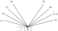
The controller unit 30 may measure, in real time, 3 or more combinations of the illuminations directly entering the camera head 20 from the light source directions (1) to (n) shown in fig. 7 by total reflection, and exclude them from the synthesized image, thereby improving the overall image quality.
The line-scanning non-lambertian surface inspection system 1 can generate a reflectance image H1, an X-axis partial differential image H2, a Y-axis partial differential image H3, a 2-order partial differential image H4 obtained by differentiating a vertical vector (Norm) image and a curvature image 2 times, and an inspection image, thereby accurately inspecting an irregular surface and a non-lambertian surface of an object to be inspected.
Fig. 15 is a perspective view illustrating a form in which the light-transmitting plate is attached to the frame module, fig. 16 is a perspective view illustrating a state in which the light-transmitting plate and the reflecting plate are attached to the frame module, fig. 17 is a front view and a side view illustrating a form in which scattered light is emitted through the light-transmitting plate, and fig. 18 is a plan view illustrating the light-transmitting plate.
Referring to fig. 15-18, the frame module 110 of the line-scan non-lambertian surface inspection system 1 further includes a transparent plate 114 and an auxiliary illumination module 125.
The transparent plate 114 is mounted in the photographing hole 112, and a Dot pattern (Dot pattern) for reflecting light in a lower direction is formed on an upper side surface.
The auxiliary lighting modules 125 are installed at a side surface of the light-transmitting plate 114 to irradiate light to the inside of the light-transmitting plate 114.
Wherein the brightness of the auxiliary lighting module 125 is adjusted by the controller portion 20.
The above-described structure can be more effectively reduced in size than the conventional method of indirectly and manually using scattered light through the dome-shaped frame module 110, and can directly control the intensity (illuminance) of the scattered light alone, thereby more effectively controlling noise in the surface inspection image.
Noise in the surface inspection image includes Dark Current Noise (Dark Current Noise) generated under low illumination conditions of the camera sensor and shot Noise (shot Noise) due to fine uneven characteristics of the surface of the product.
In the case of too little reflected light at the surface of the product, the whole image becomes dark, and dark current generated due to the low light sensitivity of the sensor causes light of a vertical component that requires a certain amount or more.
Dark current noise can be reduced by supplementing light in the vertical direction with parallel scattered light.
In addition, when the surface of the product exhibits a large difference in scattered light due to a fine polished state or a fine defect (within 1 to 2 μm), the surface defect (a mark or scratch of 10 μm or more) which is actually required to be inspected is difficult to detect, and the shot noise as described above is attenuated by the parallel scattered light illumination, and an image after the noise is removed is presented.
Therefore, the invention can remove noise by using the active scattered light when acquiring the reflectivity image, and can adjust the separately separated active scattered light, so that the image of the curvature (curvature radius/differential) image is smaller.
Thereby, an excellent surface inspection image can be obtained.
By Mie Scattering theory, light Scattering is the Scattering of light when it strikes an irregular surface below a certain size, and Mie Scattering occurs when the particles are similar to the wavelength of light or reach below a certain size.
The intensity of the scattered light depends on the angle of incidence of the light.
In order to accurately calculate the surface roughness of the inspection object, the calculation may be performed using the maxwell equation.
When the incident light is scattered on the surface of the inspection object, the density M of the particles and the brightness of the scattered light satisfy the following formula.
Figure BDA0003282468920000151
Where γ is the distance between the camera and the object under examination, ρ is the density of small particles on the surface, lkIs the brightness of the scattered wavelength k, ik0Is the brightness, λ, of incident light of wavelength kkThe wavelength k of the incident light, S, is the surface area of the inspection object.
Furthermore, lk1And lk2Is the vertical and horizontal polarization components of the scattered light, which is the refractive index of the objectnA function related to the scattering angle theta.
α(Di) M is the number of different distribution functions for the surface particle distribution function of the examination object.
The concentration of surface particles has a linear relationship with the brightness of the scattered light.
The present invention is designed to appropriately adjust the distance from the camera and the brightness of the auxiliary lighting module on the basis of the formula, thereby maximizing the difference between the brightness of light scattered due to the inherent surface roughness of the inspection object and the brightness due to the surface defect.
When the surface of the inspection object is contaminated by welding but is not defective, or the surface is in a dirty state due to the buckling of the surface but is not classified as defective, there is a possibility that the defect such as a scratch or a puncture occurring in the surface cannot be distinguished.
In the present invention, it is possible to acquire an image while adjusting the brightness of the auxiliary lighting module and to detect the contamination or surface buckling due to welding as described above from the defect by using the image.
Fig. 19 is an explanatory diagram illustrating an image difference (a: illumination without scattered light, b: illumination with scattered light) in relation to whether scattered light illumination is applied or not.
The (a) image in fig. 19 is an image taken without the scattered light system, and the (b) image is a result of synthesis using scattered light.
In the image shown in fig. 19, a lighter portion is a scratch or a poor puncture, and a darker portion is the surface of the inspection target object.
(a) The image and (b) the image have almost no brightness change, but as the illumination of the auxiliary illumination module becomes brighter, the brightness of the surface of the object becomes brighter.
Therefore, a portion where the luminance change of the illumination is small is extracted as a defect (scratch or stab mark).
In principle, when the size D of the surface particles of the inspection target object is within the Mie Scattering (Mie Scattering), there is a linear relationship between the surface luminance of the inspection target object and the luminance of the auxiliary lighting module, but when the size D of the particles is larger than the Mie Scattering (Mie Scattering) range (e.g., a scratch or a puncture), there is almost no relationship with the luminance of the auxiliary lighting module.
Fig. 20 is an illustrative view illustrating a process of detecting a scratch and a stab mark.
Referring to fig. 20, as the brightness of the Diffuse reflection Module (Diffuse Module), after the Image 0(Image 0) is acquired from the Intensity 0(Intensity 0) and the Image n (Image n) is acquired from the Intensity n (Intensity n), the difference between the Image 0(Image 0) and the Image n (Image n) is calculated, and the Scratch (Scratch) and the stamp mark are detected from the images.
FIG. 21 is a graph relating to whether scattered light is present or absent (a: noise is serious, b: noise has been removed).
The green line in fig. 21 is the outline of the corresponding image.
As can be seen from the profile of the image (b) in fig. 21, the standard deviation value decreases from 20 to 15.
FIG. 22 is a histogram of the surface histogram with respect to the presence or absence of scattered light (a: higher deviation due to smoothing and b: lower deviation due to lower smoothing).
It can be known from the histogram of the green region that the base noise information can be greatly reduced by the scattered light, so that the standard deviation value is reduced from the original 23 to 15.
Although the embodiments of the present invention have been described above with reference to the drawings, it will be understood by those having ordinary skill in the art to which the present invention pertains that the present invention may be embodied in other specific forms without changing its technical or essential features. The embodiments described in the foregoing are therefore to be considered in all respects only as illustrative and not restrictive.

Claims (4)

1.一种行扫描用非郎伯表面检查系统,包括:1. A non-Lambertian surface inspection system for line scanning, comprising: 表面检查部(10),在一侧面以及另一侧面中的至少一个上形成曲线形的搁置孔(111),包括在上端形成拍摄孔(112)的框架模块(110)以及通过在搁置孔(111)中安装多个而向放置在底面上的被检查物体(A)沿着斜线照射光线的第一照明模块(121)以及第二照明模块(122);The surface inspection part (10) has a curvilinear rest hole (111) formed on at least one of one side surface and the other side surface, comprises a frame module (110) with a shooting hole (112) formed at the upper end, In 111), a plurality of first lighting modules (121) and second lighting modules (122) are installed to irradiate light along an oblique line to the inspected object (A) placed on the bottom surface; 摄像头部(20),位于拍摄孔(112)的上方,通过贯通拍摄孔(112)并对位于底面(B)上的被检查物体(A)进行拍摄而生成包括第一照明图像(E1)以及第二照明图像(E2)在内的整体合成图像(C);以及,The camera head (20) is located above the shooting hole (112), and generates a first illumination image (E1) including a first illumination image (E1) and the overall composite image (C) including the second illumination image (E2); and, 控制器部(30),用于对摄像头部(20)的工作进行控制,通过选择性地驱动第一照明模块(121)以及第二照明模块(122)工作而从通过摄像头部(20)拍摄到的整体接收图像(C)提取出第一照明图像(E1)以及第二照明图像(E2)并利用预先设定的公式加工之后进行合成而生成合成图像(H1~H4);The controller part (30) is used for controlling the operation of the camera head (20), and by selectively driving the first lighting module (121) and the second lighting module (122) to operate, so as to shoot through the camera head (20) The obtained overall received image (C) extracts the first illumination image (E1) and the second illumination image (E2) and processes them using a preset formula, and then combines them to generate composite images (H1-H4); 控制器部(30),controller section (30), 在设定时间内打开第一照明模块(121)之后再将其关闭,After turning on the first lighting module (121) within a set time, then turning it off, 在关闭第一照明模块(121)时打开第二照明模块(122),turning on the second lighting module (122) while turning off the first lighting module (121), 在第一照明模块(121)被打开时接收通过摄像头部(20)拍摄到的第一照明图像(E1),receiving a first lighting image (E1) captured by the camera head (20) when the first lighting module (121) is turned on, 在第二照明模块(122)被打开时接收通过摄像头部(20)拍摄到的第二照明图像(E2),receiving a second lighting image (E2) captured by the camera head (20) when the second lighting module (122) is turned on, 控制器部(30),包括:The controller part (30) includes: 照明图像接收模块(310),用于将通过摄像头部(20)拍摄到的第一照明图像(E1)以及第二照明图像(E2)按照所设定的行(Row)或列(Column)的区域进行接收;The illumination image receiving module (310) is configured to receive the first illumination image (E1) and the second illumination image (E2) captured by the camera head (20) according to the set row (Row) or column (Column) area to receive; 对齐模块(320),用于对第一照明图像(E1)的多个行(Row)或列(Column)的部分图像(D1)以及第二照明图像(E2)的多个行(Row)或列(Column)的部分图像(D2)进行对齐;an alignment module (320) for aligning partial images (D1) of multiple rows (Row) or columns (Column) of the first illumination image (E1) and multiple rows (Row) or rows of the second illumination image (E2) Align part of the image (D2) of the column (Column); 直方图模块(330),用于将第一照明图像(E1)以及第二照明图像(E2)分割成多个区块(F)并在为各个区块(F)分配位置编号之后提取出区块的反射度值;A histogram module (330) for dividing the first illumination image (E1) and the second illumination image (E2) into a plurality of blocks (F) and extracting the regions after assigning position numbers to each of the blocks (F) the reflectance value of the block; 去除模块(340),通过对预先设定的基准反射度值以及从区块(F)中测定到的反射度值进行对比而删除具有与基准反射度值相比更大的反射度值的区块(F);以及,A removal module (340) for removing regions with a reflectance value greater than the reference reflectance value by comparing a preset reference reflectance value with the reflectance value measured from the block (F) block (F); and, 区块补正图像模块(350),在从第一照明图像(E1)中删除具有与基准反射度值相比更大的反射度值的区块(F)之后,从第二照明图像(E2)接收与从第一照明图像(E1)删除的区块(F)相同位置上的区块并通过映射到第一照明图像(E1)而生成第一区块补正图像(G1),A block correction image module (350), after deleting from the first illumination image (E1) a block (F) with a reflectance value greater than the reference reflectance value, from the second illuminated image (E2) receiving a block on the same position as the block (F) deleted from the first illumination image (E1) and generating a first block correction image (G1) by mapping to the first illumination image (E1), 在从第二照明图像(E2)中删除具有与基准反射度值相比更大的反射度值的区块(F)之后,从第一照明图像(E1)接收与从第二照明图像(E2)删除的区块(F)相同位置上的区块并通过映射到第二照明图像(E1)而生成第二区块补正图像(G2);After deleting from the second illumination image (E2) the block (F) with a reflectance value that is greater than the reference reflectance value, receiving from the first illumination image (E1) and from the second illumination image (E2 ) block on the same position of the deleted block (F) and generate the second block correction image (G2) by being mapped to the second illumination image (E1); 控制器部(30),还包括:The controller part (30) also includes: 合成图像生成模块(360),通过按照预先设定的算式对第一区块补正图像(G1)以及第二区块补正图像(G2)进行演算之后再进行合成而生成合成图像(H);Synthesized image generation module (360), by synthesizing the first block correction image (G1) and the second block correction image (G2) according to a preset calculation formula and then synthesizing to generate a combined image (H); 合成图像生成模块(360),a composite image generation module (360), 在合成图像(H)的设定区域中加工成反射率图像(H1),The reflectance image (H1) is processed in the set area of the composite image (H), 或在合成图像(H)中沿着X轴方向计算出被检查物体的表面高度的变化量并加工成X轴偏微分图像(H2),Or in the composite image (H), the variation of the surface height of the inspected object is calculated along the X-axis direction and processed into the X-axis partial differential image (H2), 或加工成在合成图像(H)中沿着Y轴方向计算出被检查物体的表面高度的变化量的Y轴偏微分图像(H3),Or processed into a Y-axis partial differential image (H3) in which the amount of change in the surface height of the inspected object is calculated along the Y-axis direction in the composite image (H), 或加工成将X轴偏微分图像(H2)以及Y轴偏微分图像(H3)沿着X轴方向以及Y轴方向计算出被检查物体的表面高度的变化量的2此偏微分图像(H4)。Or processed into two partial differential images (H4) in which the amount of change in the surface height of the object to be inspected is calculated along the X-axis and Y-axis directions from the X-axis partial differential image (H2) and the Y-axis partial differential image (H3). . 2.根据权利要求1所述的行扫描用非郎伯表面检查系统,2. The non-Lambert surface inspection system for line scanning according to claim 1, 框架模块(110),frame module (110), 以包含于半球形中的形状形成。Formed in a shape contained in a hemisphere. 3.根据权利要求1所述的行扫描用非郎伯表面检查系统,3. The non-Lambert surface inspection system for line scanning according to claim 1, 框架模块(110),还包括:A frame module (110), further comprising: 反射板(113),安装在上侧面。The reflector (113) is installed on the upper side. 4.根据权利要求1所述的行扫描用非郎伯表面检查系统,4. The non-Lambert surface inspection system for line scanning according to claim 1, 所述框架模块(110),还包括:The frame module (110) further includes: 透光板,安装在所述拍摄孔(112)中且在上侧面形成有用于将光线反射到下部方向的光点图形;以及,a light-transmitting plate, which is installed in the shooting hole (112) and has a light spot pattern formed on the upper side for reflecting light to the lower direction; and, 辅助照明模块(125),通过在所述透光板(114)的侧面安装多个而向所述透光板(114)的内部照射光线;Auxiliary lighting modules (125) for irradiating light to the interior of the light-transmitting plate (114) by installing a plurality of them on the side surface of the light-transmitting plate (114); 所述辅助照明(125),the auxiliary lighting (125), 通过所述控制器部(20)对其亮度进行调节。Its brightness is adjusted by the controller part (20).
CN202111137167.9A 2020-09-28 2021-09-27 Non-lambert surface inspection system for line scanning Pending CN114324344A (en)

Applications Claiming Priority (2)

Application Number Priority Date Filing Date Title
KR10-2020-0126330 2020-09-28
KR1020200126330A KR102216999B1 (en) 2020-09-28 2020-09-28 Non-Lambertian Surface Inspecting System For Line Scan

Publications (1)

Publication Number Publication Date
CN114324344A true CN114324344A (en) 2022-04-12

Family

ID=74688485

Family Applications (1)

Application Number Title Priority Date Filing Date
CN202111137167.9A Pending CN114324344A (en) 2020-09-28 2021-09-27 Non-lambert surface inspection system for line scanning

Country Status (5)

Country Link
US (1) US11657495B2 (en)
EP (1) EP3974817B1 (en)
JP (1) JP7578241B2 (en)
KR (1) KR102216999B1 (en)
CN (1) CN114324344A (en)

Families Citing this family (3)

* Cited by examiner, † Cited by third party
Publication number Priority date Publication date Assignee Title
JP6736798B1 (en) * 2020-02-14 2020-08-05 ヤマザキマザック株式会社 Work setting method for work device, work setting support system, and work setting support program
KR102368707B1 (en) * 2021-09-07 2022-02-28 주식회사 하이브비젼 Non-Lambertian Surface Inspecting System For Line Scan
KR102868831B1 (en) * 2023-08-10 2025-10-13 주식회사 힘스 Metal mask surface defect detecting system and detecting method

Citations (8)

* Cited by examiner, † Cited by third party
Publication number Priority date Publication date Assignee Title
JPH11118725A (en) * 1997-10-14 1999-04-30 Hitachi Electron Eng Co Ltd Defect inspection equipment
US20100245813A1 (en) * 2009-03-24 2010-09-30 Orbotech Ltd. Multi-modal imaging
US20110292406A1 (en) * 2008-10-28 2011-12-01 3Shape A/S Scanner with feedback control
US20120307041A1 (en) * 2011-06-01 2012-12-06 Nariaki Fujiwara Image acquisition apparatus, pattern inspection apparatus, and image acquisition method
CN110554054A (en) * 2019-09-05 2019-12-10 西安多维机器视觉检测技术有限公司 three-dimensional blade breakage detection system of mechanically-clamped indexable turning tool
KR20200014863A (en) * 2018-08-01 2020-02-11 주식회사 뷰온 An Apparatus and Method for Inspecting Surface Defect using Image Sensor
CN110823902A (en) * 2018-08-14 2020-02-21 由田新技股份有限公司 Light source module and optical detection system
KR102135472B1 (en) * 2020-02-03 2020-07-20 주식회사 하이브비젼 System For Inspecting Of Non-Lambertian Surface

Family Cites Families (10)

* Cited by examiner, † Cited by third party
Publication number Priority date Publication date Assignee Title
KR100824808B1 (en) 2006-08-25 2008-04-24 주식회사 엘티케이 Electrode tab automatic tester for lithium secondary battery
TWI359245B (en) * 2008-10-27 2012-03-01 Univ Chung Hua Machine vision inspection system and light source
KR20100135472A (en) * 2009-06-17 2010-12-27 (주)일래스틱네트웍스 Strap for Body Attachment
JP4762369B2 (en) * 2009-12-08 2011-08-31 パナソニック株式会社 Image processing device
WO2012159109A2 (en) * 2011-05-19 2012-11-22 Bir Bhanu Dynamic bayesian networks for vehicle classification in video
FR3026217B1 (en) * 2014-09-19 2019-07-26 Norou N'doye PERCUSSION INSTRUMENT STRUCTURE SAID "CAJON"
CN106124518A (en) * 2016-07-26 2016-11-16 东莞乐视自动化科技有限公司 A multi-angle line light source for detection
JP6912824B2 (en) * 2016-11-09 2021-08-04 株式会社ブイ・テクノロジー Optical inspection equipment
CN107945152A (en) * 2017-10-27 2018-04-20 深圳市创科自动化控制技术有限公司 The defects of industrial camera detecting and controlling system and method
JP6859962B2 (en) * 2018-01-10 2021-04-14 オムロン株式会社 Image inspection equipment and lighting equipment

Patent Citations (8)

* Cited by examiner, † Cited by third party
Publication number Priority date Publication date Assignee Title
JPH11118725A (en) * 1997-10-14 1999-04-30 Hitachi Electron Eng Co Ltd Defect inspection equipment
US20110292406A1 (en) * 2008-10-28 2011-12-01 3Shape A/S Scanner with feedback control
US20100245813A1 (en) * 2009-03-24 2010-09-30 Orbotech Ltd. Multi-modal imaging
US20120307041A1 (en) * 2011-06-01 2012-12-06 Nariaki Fujiwara Image acquisition apparatus, pattern inspection apparatus, and image acquisition method
KR20200014863A (en) * 2018-08-01 2020-02-11 주식회사 뷰온 An Apparatus and Method for Inspecting Surface Defect using Image Sensor
CN110823902A (en) * 2018-08-14 2020-02-21 由田新技股份有限公司 Light source module and optical detection system
CN110554054A (en) * 2019-09-05 2019-12-10 西安多维机器视觉检测技术有限公司 three-dimensional blade breakage detection system of mechanically-clamped indexable turning tool
KR102135472B1 (en) * 2020-02-03 2020-07-20 주식회사 하이브비젼 System For Inspecting Of Non-Lambertian Surface

Also Published As

Publication number Publication date
EP3974817A1 (en) 2022-03-30
US20220101516A1 (en) 2022-03-31
JP2022055348A (en) 2022-04-07
EP3974817B1 (en) 2026-03-11
KR102216999B1 (en) 2021-02-18
JP7578241B2 (en) 2024-11-06
US11657495B2 (en) 2023-05-23

Similar Documents

Publication Publication Date Title
US10805552B2 (en) Visual inspection device and illumination condition setting method of visual inspection device
CN108445007B (en) Detection method and detection device based on image fusion
US10591285B2 (en) Image inspection apparatus
JP4719284B2 (en) Surface inspection device
CN111693549A (en) Method for detecting and classifying defects of mobile phone cover plate glass
KR101679205B1 (en) Device for detecting defect of device
CN114324344A (en) Non-lambert surface inspection system for line scanning
CN111175227B (en) Device for inspecting glass substrates
KR101630596B1 (en) Photographing apparatus for bottom of car and operating method thereof
CN110208269B (en) Method and system for distinguishing foreign matter on glass surface from foreign matter inside
US20140152808A1 (en) Method and device for the reliable detection of material defects in transparent material
TWI495867B (en) Application of repeated exposure to multiple exposure image blending detection method
JP3185559B2 (en) Surface defect inspection equipment
JP2015068668A (en) Appearance inspection device
JP6917780B2 (en) Image inspection equipment
TWI884194B (en) Laser based inclusion detection system, methods, and apparatus
CN107037053B (en) Apparatus and method for detecting speckle defects
KR102678467B1 (en) Optical inspection device and method of optical inspection
TWI512284B (en) Bubble inspection system for glass
JP2009097977A (en) Appearance inspection device
KR102368707B1 (en) Non-Lambertian Surface Inspecting System For Line Scan
JP2014052339A (en) Surface irregularity inspection device and surface irregularity inspection method
TWI510776B (en) Bubble inspection processing method for glass
JP6752670B2 (en) Inspection method and equipment for transparent materials
JP4967132B2 (en) Defect inspection method for object surface

Legal Events

Date Code Title Description
PB01 Publication
PB01 Publication
SE01 Entry into force of request for substantive examination