Detailed Description
Hereinafter, in order to explain the present invention in more detail, a mode for carrying out the present invention will be described with reference to the drawings.
Embodiment mode 1
Fig. 1 is a block diagram showing a communication device including the doherty amplifier 1 of embodiment 1.
In fig. 1, a doherty amplifier 1 divides a communication signal into a 1 st signal and a 2 nd signal, and amplifies the 1 st signal and the 2 nd signal, respectively.
Fig. 2 is a block diagram showing the doherty amplifier 1 of embodiment 1.
In fig. 2, the input terminal 11 is a terminal to which a communication signal is input.
The input matching circuit 12 is realized by, for example, a circuit using lumped constant elements, a circuit using distributed constant lines, a circuit combining lumped constants and distributed constants, an L-C type matching circuit using a coil and a capacitor, or quarter wavelength lines.
One end of the input matching circuit 12 is connected to the input terminal 11, and the other end of the input matching circuit 12 is connected to the input terminal 13a of the distributor 13.
The input matching circuit 12 converts the impedance of the input terminal 11 into the input impedance of the divider 13, and outputs the communication signal input from the input terminal 11 to the divider 13.
The divider 13 is realized, for example, by a wilkinson divider or a hybrid circuit.
The input terminal 13a of the distributor 13 is connected to the other end of the input matching circuit 12.
An output terminal 13b of the distributor 13 is connected to one end of the phase correction circuit 14, and an output terminal 13c of the distributor 13 is connected to one end of the input matching circuit 16.
The distributor 13 distributes the communication signal output from the input matching circuit 12 into the 1 st signal and the 2 nd signal, outputs the 1 st signal to the phase correction circuit 14 from the output terminal 13b, and outputs the 2 nd signal to the input matching circuit 16 from the output terminal 13 c.
The phase correction circuit 14 is realized by, for example, a circuit using lumped constant elements, a circuit using distributed constant lines, a circuit combining lumped constants and distributed constants, an L-C type matching circuit, or quarter wavelength lines.
The phase correction circuit 14 is a circuit in which the electrical length of the path on the carrier amplifier 17 side from the output terminal 13b of the divider 13 to the combining point 25 of the combining circuit 24 and the electrical length of the path on the peak amplifier 18 side from the output terminal 13c of the divider 13 to the combining point 25 are aligned to be the same electrical length.
However, the electrical length of the path on the carrier amplifier 17 side and the electrical length of the path on the peak amplifier 18 side are not limited to exactly the same electrical length, and may be different from each other in a range that is not problematic in terms of practical use.
The input matching circuit 15 is realized by, for example, a circuit using lumped constant elements, a circuit using distributed constant lines, a circuit combining lumped constants and distributed constants, an L-C type matching circuit, or a quarter wavelength line.
One end of the input matching circuit 15 is connected to the other end of the phase correction circuit 14, and the other end of the input matching circuit 15 is connected to an input terminal 17a of the carrier amplifier 17.
The input matching circuit 15 converts the impedance of the phase correction circuit 14 into the input impedance of the carrier amplifier 17, and outputs the 1 st signal output from the phase correction circuit 14 to the input terminal 17a of the carrier amplifier 17.
The input matching circuit 16 is realized by, for example, a circuit using lumped constant elements, a circuit using distributed constant lines, a circuit combining lumped constants and distributed constants, an L-C type matching circuit, or quarter wavelength lines.
One end of the input matching circuit 16 is connected to the output terminal 13c of the distributor 13, and the other end of the input matching circuit 16 is connected to the input terminal 18a of the peak amplifier 18.
The input matching circuit 16 converts the impedance of the output terminal 13c of the divider 13 into the input impedance of the peak amplifier 18, and outputs the 2 nd signal output from the output terminal 13c of the divider 13 to the input terminal 18a of the peak amplifier 18.
The carrier amplifier 17 is realized by, for example, a FET (Field Effect Transistor), HBT (Heterojunction Bipolar Transistor), or HEMT (High Electron Mobility Transistor).
In the doherty amplifier 1 shown in fig. 2, an example is shown in which the carrier amplifier 17 is a transistor whose source is grounded. The input terminal 17a of the carrier amplifier 17, i.e., the gate terminal, is connected to the other end of the input matching circuit 15, and the output terminal 17b of the carrier amplifier 17, i.e., the drain terminal, is connected to one end of the 1 st output circuit 19. The 1 st output circuit 19 will be described later.
The input terminal 17a of the carrier amplifier 17 is biased between the a stage and the B stage.
The carrier amplifier 17 has a nonlinear output capacitor, amplifies the 1 st signal output from the input matching circuit 15, and outputs the amplified 1 st signal to the 1 st output circuit 19.
When the carrier amplifier 17 is represented by an equivalent circuit, the carrier amplifier 17 can be represented by a current source 31 and a capacitor 32 having an output capacitance.
The peak amplifier 18 is realized by, for example, an FET, HBT, or HEMT.
In the doherty amplifier 1 shown in fig. 2, an example is shown in which the peak amplifier 18 is a transistor whose source is grounded. The input terminal 18a, i.e., the gate terminal, of the peak amplifier 18 is connected to the other end of the input matching circuit 16, and the output terminal 18b, i.e., the drain terminal, of the peak amplifier 18 is connected to one end of the 2 nd output circuit 20. The 2 nd output circuit 20 will be described later.
The input terminal 18a of the peak amplifier 18 is biased at stage C.
The peak amplifier 18 amplifies the 2 nd signal output from the input matching circuit 16, and outputs the amplified 2 nd signal to the 2 nd output circuit 20.
When the peak amplifier 18 is represented by an equivalent circuit, the peak amplifier 18 can be represented by a current source 41 and a capacitor 42 having an output capacitance.
The capacitor 42 has an output capacitance that increases non-linearly with an increase in the output power of the peak amplifier 18.
The peak amplifier 18 functions as follows: the inductive component of the impedance when the combining circuit 24 is viewed from the peak amplifier 18 is reduced by the nonlinear output capacitance of the peak amplifier.
The 1 st output circuit 19 is realized, for example, by a transmission line having an electrical length of less than 90 degrees.
One end of the 1 st output circuit 19 is connected to the output terminal 17b of the carrier amplifier 17, and the other end of the 1 st output circuit 19 is connected to the input terminal 24a of the combining circuit 24.
The 1 st output circuit 19 transmits the 1 st signal output from the carrier amplifier 17, and outputs the 1 st signal to the combining circuit 24.
The 1 st output circuit 19 has an electrical length of less than 90 degrees that compensates for the reactive power of the 2 nd output circuit 20 when viewed from the output side of the carrier amplifier 17 when the peak amplifier 18 does not perform an amplifying operation.
The characteristic impedance of the 1 st output circuit 19 coincides with the optimum load impedance Ropt when the output power of the carrier amplifier 17 is saturated. However, the characteristic impedance of the 1 st output circuit 19 is not limited to strictly match the optimum load impedance Ropt, and may be shifted from the optimum load impedance Ropt within a range that does not pose a practical problem.
The 2 nd output circuit 20 has an electrical length larger than 90 degrees and smaller than 180 degrees, and has the transmission line 21 and the transmission line 23 as 2 transmission lines. The connection point 22 is a point connecting the transmission line 21 and the transmission line 23.
In the doherty amplifier shown in fig. 2, the 2 nd output circuit 20 has a transmission line 21 and a transmission line 23. However, this is merely an example, and the 2 nd output circuit 20 may be realized by 1 transmission line in which the transmission line 21 and the transmission line 23 are integrally formed.
One end of the 2 nd output circuit 20 is connected to the output terminal 18b of the peak amplifier 18, and the other end of the 2 nd output circuit 20 is connected to the input terminal 24b of the combining circuit 24.
The 2 nd output circuit 20 transfers the 2 nd signal output from the peak amplifier 18, and outputs the 2 nd signal to the synthesizing circuit 24.
The characteristic impedance of the 2 nd output circuit 20 coincides with the optimum load impedance Ropt when the output power of the peak amplifier 18 is the saturated output power. However, the characteristic impedance of the 2 nd output circuit 20 is not limited to strictly match the optimum load impedance Ropt, and may be shifted from the optimum load impedance Ropt within a range that does not pose a practical problem.
Here, the 2 nd output circuit 20 is shown to have an electrical length greater than 90 degrees and less than 180 degrees. However, this is merely an example, and the 2 nd output circuit 20 may have an electrical length greater than-90 degrees and less than 0 degrees at the left-hand rule. In the case where the 2 nd output circuit 20 has an electrical length greater than-90 degrees and less than 0 degrees at the left-hand rule, the 2 nd output circuit 20 has a filter circuit at the left-hand rule.
The 2 nd output circuit 20 changes the impedance when the peak amplifier 18 is viewed from the combining circuit 24 to the impedance of the inductive region when the peak amplifier 18 performs the amplification operation.
The 2 nd output circuit 20 forms a short-circuit point between the peak amplifier 18 and the combining circuit 24, that is, a connection point 22, at the time of a back-off when the peak amplifier 18 is stopped.
When the peak amplifier 18 outputs a power lower than the saturated output power, the 2 nd output circuit 20 changes the impedance when the combining circuit 24 is viewed from the peak amplifier 18 to the impedance of the inductive region, based on the back-off amount of the peak amplifier 18.
At this time, the peak amplifier 18 reduces the inductive component of the impedance when the synthesizing circuit 24 is viewed from the peak amplifier 18, based on the output capacitance of the capacitor 42.
The transmission line 21 has an electrical length of 90 degrees.
One end of the transmission line 21 is connected to the output terminal 18b of the peak amplifier 18, and the other end of the transmission line 21 is connected to the connection point 22.
The transmission line 23 has an electrical length of less than 90 degrees.
One end of the transmission line 23 is connected to the connection point 22, and the other end of the transmission line 23 is connected to the input terminal 24b of the synthesis circuit 24.
The combining circuit 24 has a combining point 25 that combines the 1 st signal output from the 1 st output circuit 19 and the 2 nd signal output from the 2 nd output circuit 20.
The input terminal 24a of the combining circuit 24 is connected to the other end of the 1 st output circuit 19.
The input terminal 24b of the combining circuit 24 is connected to the other end of the transmission line 23.
The synthesizing circuit 24 synthesizes the 1 st signal output from the 1 st output circuit 19 and the 2 nd signal output from the 2 nd output circuit 20.
The synthesizing circuit 24 outputs a synthesized signal of the 1 st signal and the 2 nd signal to the output matching circuit 26.
The combining point 25 is a combining point of the 1 st signal output from the 1 st output circuit 19 and the 2 nd signal output from the 2 nd output circuit 20. One end of an output matching circuit 26 is connected to the combining point 25.
The output matching circuit 26 is realized by, for example, a circuit using lumped constant elements, a circuit using distributed constant lines, a circuit combining lumped constants and distributed constants, an L-C type matching circuit, or quarter wavelength lines.
One end of the output matching circuit 26 is connected to the combining point 25, and the other end of the output matching circuit 26 is connected to a load 27 outside the doherty amplifier 1.
The output matching circuit 26 converts the impedance of the combining point 25 into the impedance of the load 27.
The load 27 is a load external to the doherty amplifier 1 connected to the other end of the output matching circuit 26.
Next, the operation of the doherty amplifier 1 shown in fig. 2 will be described.
Upon receiving the communication signal input from the input terminal 11, the input matching circuit 12 converts the impedance of the input terminal 11 into the input impedance of the distributor 13, and outputs the communication signal to the distributor 13.
Upon receiving the communication signal from the input matching circuit 12, the distributor 13 distributes the communication signal into the 1 st signal and the 2 nd signal.
The distributor 13 outputs the 1 st signal from the output terminal 13b to the phase correction circuit 14, and outputs the 2 nd signal from the output terminal 13c to the input matching circuit 16.
The phase correction circuit 14 receives the 1 st signal from the output terminal 13b of the distributor 13, and outputs the 1 st signal to the input matching circuit 15.
At this time, the phase correction circuit 14 functions as follows: the electrical length of the path on the carrier amplifier 17 side from the output terminal 13b of the distributor 13 to the combining point 25 and the electrical length of the path on the peak amplifier 18 side from the output terminal 13c of the distributor 13 to the combining point 25 are aligned to be the same electrical length.
The input matching circuit 15 receives the 1 st signal from the phase correction circuit 14, converts the impedance of the phase correction circuit 14 into the input impedance of the carrier amplifier 17, and outputs the 1 st signal to the input terminal 17a of the carrier amplifier 17.
The carrier amplifier 17 receives the 1 st signal from the input matching circuit 15, amplifies the 1 st signal, and outputs the amplified 1 st signal to the 1 st output circuit 19.
The 1 st output circuit 19 receives the amplified 1 st signal from the carrier amplifier 17, transmits the 1 st signal, and outputs the 1 st signal to the combining circuit 24.
The input matching circuit 16 receives the 2 nd signal from the output terminal 13c of the divider 13, converts the impedance of the output terminal 13c of the divider 13 into the input impedance of the peak amplifier 18, and outputs the 2 nd signal to the input terminal 18a of the peak amplifier 18.
The peak amplifier 18 receives the 2 nd signal from the input matching circuit 16, amplifies the 2 nd signal, and outputs the amplified 2 nd signal to the 2 nd output circuit 20.
The 2 nd output circuit 20 receives the amplified 2 nd signal from the peak amplifier 18, transmits the 2 nd signal, and outputs the 2 nd signal to the combining circuit 24.
The synthesizing circuit 24 synthesizes the 1 st signal output from the 1 st output circuit 19 and the 2 nd signal output from the 2 nd output circuit 20.
The synthesizing circuit 24 outputs a synthesized signal of the 1 st signal and the 2 nd signal to the output matching circuit 26.
The output matching circuit 26 receives the synthesized signal from the synthesizing circuit 24, converts the impedance of the synthesizing point 25 into the impedance of the external load 27, and outputs the synthesized signal to the load 27.
Next, the operation of the doherty amplifier 1 in the back-off state in which the peak amplifier 18 is stopped will be described.
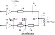
Fig. 3 is an explanatory diagram showing an operation in the back-off of the doherty amplifier 1. In fig. 3, the output matching circuit 26 is not shown.
Fig. 4 is an explanatory diagram showing a load change in the operation at the time of the back-off of the doherty amplifier 1.
At the time of back-off, the peak amplifier 18 is stopped, and therefore, as shown in fig. 3, the output impedance of the peak amplifier 18 is in an open state.
The output impedance of the peak amplifier 18 is changed by a transmission line 21 having an electrical length of 90 degrees, and a short-circuit point is formed at a connection point 22.
Since the short-circuit point is formed at the connection point 22, the transmission line 23 functions as a virtual short-circuited stub when the peak amplifier 18 is viewed from the combining point 25.
The transmission line 23 functions as a virtual short stub, and thus, as shown in fig. 4, the impedance Γ when the load 27 is viewed from the combining point 251I.e. the output load Ropt becomes the impedance Γ2。
As shown in fig. 4, the impedance Γ2Impedance gamma on the real axis is changed by the 1 st output circuit 193。
Impedance gamma3The output load impedance of the carrier amplifier 17 is larger than the output load impedance 2 × Ropt of the carrier amplifier in the general doherty amplifier. The general doherty amplifier here refers to the saturated output power and peak amplifier of the carrier amplifierThe doherty amplifier having the same saturated output power of (1) is a doherty amplifier having a back-off of 6 dB.
Therefore, the back-off of the doherty amplifier 1 shown in fig. 2 can be made larger than that of a general doherty amplifier.
Next, the operation of the doherty amplifier 1 when the peak amplifier 18 outputs a power lower than the saturated output power will be described.
Fig. 5 is an explanatory diagram showing the operation of the doherty amplifier 1 when the peak amplifier 18 outputs a power lower than the saturated output power. In fig. 5, the output matching circuit 26 is not shown.
Fig. 6 is an explanatory diagram showing a load change of the doherty amplifier 1 when the peak amplifier 18 outputs a power lower than the saturated output power.
First, as shown in the following expressions (1) and (3), the electrical length EL of the 1 st output circuit 19 is determined in accordance with the desired back-off OBO1。
As shown in the following expressions (2) and (3), the electrical length EL of the 2 nd output circuit 20 is determined in accordance with the desired back-off OBO2。
OBO=10logy[dB] (3)
As for the output load impedance of the carrier amplifier 17, the load varies in accordance with the output power of the peak amplifier 18. Specifically, as for the output load impedance of the carrier amplifier 17, the load is selected from the impedance Γ on the real axis as shown in fig. 63Varying to impedance on the real axis0. Impedance gamma0Is the optimum load impedance Ropt when the output power of the carrier amplifier 17 is the saturated output power.
The output load impedance of the peak amplifier 18 varies as follows.
Here, for convenience of explanation, as shown in fig. 5, the output capacitance of the peak amplifier 18, that is, the output capacitance of the capacitor 42 is divided into a capacitor 43 having an output capacitance when the signal level of the 2 nd signal is small and a capacitor 44 having an increased amount of the output capacitance which increases as the signal level of the 2 nd signal increases.
When the peak amplifier 18 outputs a power lower than the saturated output power, as shown in fig. 6, the impedance Γ when the combining point 25 is viewed from the transmission line 235Is the impedance of the capacitive region.
Impedance gamma5The impedance of the transmission line 23 changes by an amount of less than 90 degrees, and the impedance when the transmission line 23 is viewed from the connection point 22 becomes Γ6. As shown in fig. 6, the impedance Γ6Is the impedance of the capacitive region.
Impedance gamma6Impedance changes by an amount of 90 degrees of the electrical length of the transmission line 21, and the impedance when the transmission line 21 is viewed from between the capacitor 43 and the capacitor 44 becomes Γ7。
Since the 2 nd output circuit 20 is an inductive circuit that functions as a virtual short stub at the time of back-off, the impedance Γ is as shown in fig. 67Becoming the impedance of the inductive region.
In the doherty amplifier 1 shown in fig. 2, the peak amplifier 18 includes a capacitor 44 having an increased amount of output capacitance. Thus, the impedance Γ7Impedance is changed so as to approach the real axis by the increase of the output capacitance of the capacitor 44, and the impedance when the combining point 25 is observed from the current source 41 of the peak amplifier 18 becomes Γ8。
Based on the output power of the peak amplifier 18, the impedance Γ at the combining point 25 is observed from the current source 41 of the peak amplifier 188Becomes an arbitrary impedance on the solid line shown in fig. 6. The solid line shown in fig. 6 exists in a region close to the solid axis.
Thus, during the period from the back-off when the output power of the peak amplifier 18 is zero until the output power of the peak amplifier 18 becomes the saturated output power, the load is switched from the open circuit with respect to the output load impedance of the peak amplifier 18The point is changed into the impedance Γ on the solid axis via the solid line shown in fig. 60. In fig. 6, the open point is described as "P small", which means that the output power is zero. Gamma-shaped0Is a point described as "P large," which means that the output power is the saturated output power.
In the doherty amplifier disclosed in patent document 1, when the peak amplifier outputs a power lower than the saturated output power, the impedance when the output combining point is viewed from the peak amplifier becomes the impedance of the capacitive region. The distance of the impedance from the real axis when the output combining point is viewed from the peak amplifier and the impedance Γ when the combining circuit 24 is viewed from the peak amplifier 18 shown in fig. 27' substantially equal distances from the real axis.
In the doherty amplifier disclosed in patent document 1, the capacitive component of the impedance when the output combining point is viewed from the peak amplifier is further increased by the output capacitance of the peak amplifier. Therefore, the impedance when the output combining point is viewed from the peak amplifier changes so that the distance from the real axis of the impedance when the output combining point is viewed from the peak amplifier increases, depending on the output capacitance of the peak amplifier.
In the doherty amplifier 1 shown in fig. 2, the impedance Γ of the inductive region is changed by the amount of increase in the output capacitance of the capacitor 447The perceptual component of (a) is reduced. Therefore, the impedance Γ at the combining point 25 is viewed from the current source 41 of the peak amplifier 188The distance from the real axis is smaller than the distance from the real axis of the impedance when the output combining point is viewed from the peak amplifier in the doherty amplifier disclosed in patent document 1.
Thus, in the doherty amplifier 1 shown in fig. 2, impedance change can be achieved for a region close to the real axis as compared with the doherty amplifier disclosed in patent document 1.
Fig. 7 is an explanatory diagram showing simulation results of the efficiency of the doherty amplifier 1 of embodiment 1 and the efficiency of the doherty amplifier 1 described in patent document 1.
In the doherty amplifier described in patent document 1, as shown in fig. 7, the efficiency is greatly deteriorated until the output power of the peak amplifier reaches the saturation output power from the power at which the efficiency peak occurs. That is, there is output power whose efficiency is greatly deteriorated until the output power of the peak amplifier becomes saturated output power from zero power.
In the doherty amplifier 1 of embodiment 1, there is no output power whose efficiency is greatly deteriorated until the output power of the peak amplifier 18 becomes the saturated output power from the power of zero, and the efficiency is higher than that of the doherty amplifier described in patent document 1.
In the above embodiment 1, the doherty amplifier 1 is configured as follows: when the peak amplifier 18 performs an amplifying operation, the 2 nd output circuit 20 changes the impedance when the combining circuit 24 is viewed from the peak amplifier 18 to the impedance of the inductive region. Therefore, the doherty amplifier 1 can prevent efficiency deterioration when the peak amplifier 18 outputs power lower than the saturated output power.
Embodiment mode 2
In embodiment 2, the doherty amplifier 1 in which the saturated output power of the peak amplifier 18 is larger than that of the carrier amplifier 17 will be described.
The configuration of the doherty amplifier 1 of embodiment 2 is the same as that of the doherty amplifier 1 of embodiment 1, and fig. 2 is a diagram showing the configuration of the doherty amplifier 1 of embodiment 2.
Next, the operation of the doherty amplifier 1 in the back-off state in which the peak amplifier 18 is stopped will be described.
Fig. 8 is an explanatory diagram showing an operation at the time of back-off of the doherty amplifier 1. In fig. 8, the output matching circuit 26 is not shown.
Fig. 9 is an explanatory diagram showing a load change in the operation at the time of the back-off of the doherty amplifier 1.
In the doherty amplifier 1 of embodiment 2, the optimum load impedance when the output power of the carrier amplifier 17 is saturated output power is Ropt, and the optimum load impedance when the output power of the peak amplifier 18 is saturated output power is K × Ropt. K is a value less than 1 and greater than 0.
Viewed from the point of synthesis 25Impedance at load 27 Γ1Since the combined impedance of the optimum load impedance Ropt and the optimum load impedance K × Ropt is obtained, as shown in fig. 9, the impedance is smaller than 0.5 × Ropt.
Therefore, the impedance Γ in the doherty amplifier 1 of embodiment 21Impedance Γ in doherty amplifier 1 of embodiment 1 is higher1A small impedance.
At the time of back-off, the peak amplifier 18 is stopped, and therefore, as shown in fig. 8, the output impedance of the peak amplifier 18 is in an open state.
The output impedance of the peak amplifier 18 is changed by a transmission line 21 having an electrical length of 90 degrees, and a short-circuit point is formed at a connection point 22.
Since the short-circuit point is formed at the connection point 22, the transmission line 23 functions as a virtual short-circuited stub when the peak amplifier 18 is viewed from the combining point 25.
The transmission line 23 functions as a virtual short stub, and thereby the impedance Γ when the load 27 is viewed from the combining point 251I.e. the output load L × 0.5 × Ropt becomes the impedance Γ2. L is a value less than 1 and greater than 0.
As shown in fig. 9, the impedance Γ2Impedance gamma on the real axis is changed by the 1 st output circuit 193。
Impedance gamma3The output load impedance of the carrier amplifier 17 is larger than the impedance 2 × Ropt of a general doherty amplifier with a back-off of 6 dB.
Therefore, the back-off of the doherty amplifier 1 of embodiment 2 can be made larger than that of a general doherty amplifier.
Next, the operation of the doherty amplifier 1 when the peak amplifier 18 outputs a power lower than the saturated output power will be described.
Fig. 10 is an explanatory diagram showing the operation of the doherty amplifier 1 when the peak amplifier 18 outputs a power lower than the saturated output power. In fig. 10, the output matching circuit 26 is not shown.
Fig. 11 is an explanatory diagram showing a load change of the doherty amplifier 1 when the peak amplifier 18 outputs a power lower than the saturated output power.
As for the output load impedance of the carrier amplifier 17, the load varies in accordance with the output power of the peak amplifier 18. Specifically, as for the output load impedance of the carrier amplifier 17, the load is selected from the impedance Γ on the real axis as shown in fig. 113Varying to impedance on the real axis0. Impedance gamma0Is the optimum load impedance Ropt when the output power of the carrier amplifier 17 is the saturated output power.
The output load impedance of the peak amplifier 18 varies as follows.
When the peak amplifier 18 outputs a power lower than the saturated output power, as shown in fig. 11, the impedance Γ when the combining point 25 is viewed from the transmission line 235Is the impedance of the capacitive region.
Impedance gamma5The impedance of the transmission line 23 changes by an amount of less than 90 degrees, and the impedance when the transmission line 23 is viewed from the connection point 22 becomes Γ6. As shown in FIG. 11, the impedance Γ6Is the impedance of the capacitive region.
Impedance gamma6Impedance changes by an amount of 90 degrees of the electrical length of the transmission line 21, and the impedance when the transmission line 21 is viewed from between the capacitor 43 and the capacitor 44 becomes Γ7。
Since the 2 nd output circuit 20 is an inductive circuit that functions as a dummy short stub at the time of back-off, the impedance Γ is as shown in fig. 117Becoming the impedance of the inductive region.
In the doherty amplifier 1 of embodiment 2, the peak amplifier 18 includes a capacitor 44 having an increased amount of output capacitance. Thus, the impedance Γ7Impedance is changed so as to approach the real axis by the increase of the output capacitance of the capacitor 44, and the impedance when the combining point 25 is observed from the current source 41 of the peak amplifier 18 becomes Γ8。
Based on the output power of the peak amplifier 18, the impedance Γ at the combining point 25 is observed from the current source 41 of the peak amplifier 188An arbitrary impedance is shown in the solid line in fig. 11. The solid line shown in fig. 11 exists in a region close to the solid axis.
Thus, during the period from the time when the output power of the peak amplifier 18 is back-off to zero until the output power of the peak amplifier 18 becomes saturated, the output load impedance of the peak amplifier 18 is changed from the open point to the impedance Γ on the solid axis via the solid line shown in fig. 110。
In the doherty amplifier disclosed in patent document 1, when the peak amplifier outputs a power lower than the saturated output power, the impedance when the output combining point is viewed from the peak amplifier becomes the impedance of the capacitive region. The distance of the impedance from the real axis when the output combining point is viewed from the peak amplifier and the impedance Γ when the combining circuit 24 is viewed from the peak amplifier 18 shown in fig. 27' substantially equal distances from the real axis.
In the doherty amplifier disclosed in patent document 1, the capacitive component of the impedance when the output combining point is viewed from the peak amplifier is further increased by the output capacitance of the peak amplifier. Therefore, the impedance when the output combining point is viewed from the peak amplifier changes so that the distance from the real axis of the impedance when the output combining point is viewed from the peak amplifier increases, depending on the output capacitance of the peak amplifier.
In the doherty amplifier 1 of embodiment 2, the impedance Γ of the inductive region is changed in accordance with the amount of increase in the output capacitance of the capacitor 447The perceptual component of (a) is reduced. Therefore, the impedance Γ at the combining point 25 is viewed from the current source 41 of the peak amplifier 188The distance from the real axis is smaller than the distance from the real axis of the impedance when the output combining point is viewed from the peak amplifier in the doherty amplifier disclosed in patent document 1.
Thus, in the doherty amplifier 1 of embodiment 2, it is possible to realize impedance change for a region close to the real axis as compared with the doherty amplifier disclosed in patent document 1.
In the doherty amplifier 1 in which the saturated output power of the peak amplifier 18 is larger than the saturated output power of the carrier amplifier 17, similarly to the doherty amplifier 1 of embodiment 1, it is possible to prevent efficiency deterioration when the peak amplifier 18 outputs a power lower than the saturated output power.
By configuring the doherty amplifier 1 such that the saturated output power of the peak amplifier 18 is larger than the saturated output power of the carrier amplifier 17, the back-off amount at which the efficiency peak point appears can be increased as compared with the doherty amplifier 1 of embodiment 1.
Embodiment 3
In embodiment 3, a description will be given of a doherty amplifier 1 having a 1 st output matching circuit 51 and a 2 nd output matching circuit 52.
Fig. 12 is a block diagram showing a communication device including the doherty amplifier 1 of embodiment 3. In fig. 12, the same reference numerals as in fig. 2 denote the same or corresponding parts, and thus, the description thereof will be omitted.
The 1 st output matching circuit 51 is realized by, for example, a circuit using lumped constant elements, a circuit using distributed constant lines, a circuit combining lumped constants and distributed constants, an L-C type matching circuit, or quarter wavelength lines.
One end of the 1 st output matching circuit 51 is connected to the output terminal 17b of the carrier amplifier 17, and the other end of the 1 st output matching circuit 51 is connected to one end of the 1 st output circuit 19.
The 1 st output matching circuit 51 converts the output impedance of the carrier amplifier 17 into the impedance of the 1 st output circuit 19.
The 2 nd output matching circuit 52 is realized by, for example, a circuit using lumped constant elements, a circuit using distributed constant lines, a circuit combining lumped constants and distributed constants, an L-C type matching circuit, or quarter wavelength lines.
One end of the 2 nd output matching circuit 52 is connected to the output terminal 18b of the peak amplifier 18, and the other end of the 2 nd output matching circuit 52 is connected to one end of the 2 nd output circuit 20.
The 2 nd output matching circuit 52 converts the output impedance of the peak amplifier 18 into the impedance of the 2 nd output circuit 20.
The doherty amplifier 1 shown in fig. 12 is the same as the doherty amplifier 1 shown in fig. 2 except for having a 1 st output matching circuit 51 and a 2 nd output matching circuit 52.
The doherty amplifier 1 shown in fig. 12 has the 1 st output matching circuit 51, and thus can prevent the 1 st signal output from the carrier amplifier 17 from being reflected to the 1 st output circuit 19.
The doherty amplifier 1 shown in fig. 12 has the 2 nd output matching circuit 52, and thus can prevent the 2 nd signal output from the peak amplifier 18 from being reflected to the 2 nd output circuit 20.
Embodiment 4
In embodiment 4, the doherty amplifier 1 in which the bandwidth widening circuit 60 that changes the impedance when the load 27 is viewed from the combining circuit 24 is inserted between the combining circuit 24 and the load 27 will be described.
Fig. 13 is a block diagram showing the doherty amplifier 1 of embodiment 4. In fig. 13, the same reference numerals as in fig. 2 denote the same or corresponding parts, and thus, the description thereof will be omitted.
Wide bandwidth circuit 60 has transmission line 61 and open stub 62.
One end of bandwidth widening circuit 60 is connected to combining point 25 of combining circuit 24, and the other end of bandwidth widening circuit 60 is connected to one end of output matching circuit 26.
When peak amplifier 18 is stopped, if the frequency of the 1 st signal amplified by carrier amplifier 17 is shifted to a lower frequency side than the center frequency of the frequency, wideband widening circuit 60 changes the impedance when load 27 is viewed from combining circuit 24 to the impedance of the capacitive region.
If the frequency of the 1 st signal is shifted to a higher frequency side than the center frequency of the frequency, wideband widening circuit 60 changes the impedance when load 27 is viewed from combining circuit 24 to the impedance of the inductive region.
The doherty amplifier 1 shown in fig. 13 is a doherty amplifier in which the wideband-widening circuit 60 is applied to the doherty amplifier 1 shown in fig. 2. However, this is merely an example, and a doherty amplifier in which the wideband widening circuit 60 is applied to the doherty amplifier 1 shown in fig. 12 may be used.
The transmission line 61 is EL in electrical length3The line of (2).
One end of the transmission line 61 is connected to the combining point 25 of the combining circuit 24, and the other end of the transmission line 61 is connected to the connection point 63.
The electrical length EL of the 1 st output circuit 19 is subtracted from the electrical length of 90 DEG1And the resulting electrical length is thetaaElectrical length EL of transmission line 613This is represented by the following formula (4).
EL3=sin-1[2sin(2θa)] (4)
One end of the open stub 62 is connected to the connection point 63.
The electrical length of the open stub 62 is 180 degrees, and the characteristic impedance of the open stub 62 is half of the optimum load impedance Ropt when the output power of the carrier amplifier 17 is saturated.
The other end of the transmission line 61, one end of the open stub 62, and one end of the output matching circuit 26 are connected to the connection point 63.
Next, the operation of the doherty amplifier 1 shown in fig. 13 will be described. However, since the doherty amplifier is the same as the doherty amplifier 1 shown in fig. 2 except for the widening circuit 60, the operation of the widening circuit 60 will be mainly described here.
When peak amplifier 18 is stopped, if the frequency of the 1 st signal output from divider 13 is not shifted from the center frequency, wideband widening circuit 60 does not change the impedance when load 27 is viewed from combining circuit 24.
If the frequency of the 1 st signal is shifted to the low frequency side from the center frequency, wideband widening circuit 60 changes the impedance when load 27 is viewed from combining circuit 24 to the impedance of the capacitive region.
If the frequency of the 1 st signal is shifted to a higher frequency side than the center frequency, wideband widening circuit 60 changes the impedance when load 27 is viewed from combining circuit 24 to the impedance of the inductive region.
Next, the impedance change by wideband widening circuit 60 will be specifically described.
Fig. 14 is an explanatory diagram showing an operation in the back-off of the doherty amplifier 1. In fig. 14, the output matching circuit 26 is not shown.
Fig. 15 is an explanatory diagram showing a load change in the operation at the time of the back-off of the doherty amplifier 1.
At the time of back-off, the peak amplifier 18 is stopped, and therefore, as shown in fig. 14, the output impedance of the peak amplifier 18 is in an open state.
The output impedance of the peak amplifier 18 is changed by a transmission line 21 having an electrical length of 90 degrees, and a short-circuit point is formed at a connection point 22.
Since the short-circuit point is formed at the connection point 22, the transmission line 23 functions as a virtual short-circuited stub when the peak amplifier 18 is viewed from the combining point 25.
The transmission line 23 functions as a virtual short stub, and thus, as shown in fig. 15, the impedance Γ when the load 27 is viewed from the combining point 251' that is, the output load 0.5 × Ropt becomes the impedance Γ2’。
As shown in FIG. 15, the impedance Γ2' the impedance on the real axis is changed by the 1 st output circuit 193’。
Impedance gamma3' is the output load impedance of the carrier amplifier 17, which is larger than the impedance 2 × Ropt of a general doherty amplifier with a back-off of 6 dB.
Therefore, the back-off of the doherty amplifier 1 shown in fig. 13 can be made larger than that of a general doherty amplifier.
In the doherty amplifier 1 shown in fig. 13, since one end of the open stub 62 is connected to the connection point 63, if the frequency of the 1 st signal is shifted to the low frequency side from the center frequency, as shown in fig. 15, the impedance Γ when the load 27 is viewed from the other end of the transmission line 619Is the impedance of the inductive region.
If the frequency of the 1 st signal is shifted to a higher frequency side than the center frequency, the impedance Γ when the load 27 is viewed from the other end of the transmission line 61 is as shown in fig. 159Is the impedance of the capacitive region.
Impedance gamma9The impedance Γ is changed by the clockwise rotation on the smith chart shown in fig. 15 through the transmission line 611’。
At this time, if the frequency of the 1 st signal is shifted to the low frequency side from the center frequency, the impedance Γ9Impedance gamma becoming a capacitive region1'. If the frequency of the 1 st signal is shifted to the high frequency side from the center frequency, the impedance Γ9Impedance gamma becoming inductive region1’。
The transmission line 23 functions as a virtual short stub, and thereby has an impedance Γ as shown in fig. 151' become the impedance of the inductive region Γ2’。
Even if the frequency of the 1 st signal changes from a frequency on the lower frequency side of the center frequency to a frequency on the higher frequency side of the center frequency, the impedance Γ is as shown in fig. 152' also rotates only clockwise.
As shown in FIG. 15, the impedance Γ2' becomes impedance Γ by the 1 st output circuit 193'. If the wide band shaping circuit 60 is not connected to the output side of the synthesizing circuit 24, when the frequency of the 1 st signal is shifted from the center frequency, the impedance Γ is as shown in fig. 153' sometimes offset significantly from the real axis.
In the doherty amplifier 1 shown in fig. 13, since the wide band widening circuit 60 is connected to the output side of the combining circuit 24, even if the frequency of the 1 st signal is shifted from the center frequency, the impedance Γ is as shown in fig. 153' also varies roughly on the real axis.
In embodiment 4 described above, if the frequency of the 1 st signal is shifted to a lower frequency side than the center frequency when peak amplifier 18 is stopped, wideband widening circuit 60 changes the impedance when load 27 is viewed from combining circuit 24 to the impedance of the capacitive region. The doherty amplifier 1 is constructed in the following manner: if the frequency of the 1 st signal is shifted to a higher frequency side than the center frequency, wideband widening circuit 60 changes the impedance when load 27 is viewed from combining circuit 24 to the impedance of the inductive region. Therefore, the doherty amplifier 1 can prevent efficiency deterioration when the peak amplifier 18 outputs power lower than the saturated output power, similarly to the doherty amplifier 1 shown in fig. 2. Further, even if the frequency of the 1 st signal is shifted from the center frequency, efficiency deterioration when the peak amplifier 18 is stopped can be prevented.
Embodiment 5
In embodiment 5, a doherty amplifier 1 having a 1 st transmission line 71 and a 2 nd transmission line 72 will be described.
Fig. 16 is a block diagram showing the doherty amplifier 1 of embodiment 5. In fig. 16, the same reference numerals as those in fig. 2, 12, and 13 denote the same or corresponding parts, and thus, the description thereof will be omitted.
The 1 st transmission line 71 is a line having an electrical length n (n is a positive or negative integer) times 180 degrees.
One end of the 1 st transmission line 71 is connected to the other end of the 1 st output circuit 19, and the other end of the 1 st transmission line 71 is connected to the input terminal 24a of the combining circuit 24.
The 2 nd transmission line 72 is a line having an electrical length of m (m is a positive or negative integer) times 180 degrees.
One end of the 2 nd transmission line 72 is connected to the other end of the 2 nd output circuit 20, and the other end of the 2 nd transmission line 72 is connected to the input terminal 24b of the combining circuit 24.
The doherty amplifier 1 shown in fig. 16 is a doherty amplifier in which a 1 st transmission line 71 and a 2 nd transmission line 72 are applied to the doherty amplifier 1 shown in fig. 2, respectively. However, this is merely an example, and a doherty amplifier in which the 1 st transmission line 71 and the 2 nd transmission line 72 are applied to the doherty amplifier 1 shown in fig. 12 or 13 may be used.
The doherty amplifier 1 shown in fig. 16 is the same as the doherty amplifier 1 shown in fig. 2 except for the point that there are the 1 st transmission line 71 and the 2 nd transmission line 72.
In the doherty amplifier 1 shown in fig. 16, even if the 1 st transmission line 71 and the 2 nd transmission line 72 are provided, it is possible to prevent efficiency deterioration when the peak amplifier 18 outputs power lower than the saturated output power, as in the doherty amplifier 1 shown in fig. 2.
In the doherty amplifier 1 shown in fig. 16, by having the 1 st transmission line 71 and the 2 nd transmission line 72, for example, the 1 st transmission line 71 and the 2 nd transmission line 72 can be routed according to the size of a substrate on which the doherty amplifier 1 shown in fig. 16 is mounted.
Embodiment 6
In embodiment 6, a description will be given of a doherty amplifier 1 having a 1 st input signal source 81 and a 2 nd input signal source 82.
Fig. 17 is a block diagram showing the doherty amplifier 1 of embodiment 6. In fig. 17, the same reference numerals as those in fig. 2, 12, 13, and 16 denote the same or corresponding parts, and thus, the description thereof will be omitted.
The signal source 80 has a 1 st input signal source 81 and a 2 nd input signal source 82.
The signal source 80 distributes a communication signal input to the signal source 80 into 2 signals.
The signal source 80 outputs one of the 2 signals to the 1 st input signal source 81 and the other signal to the 2 nd input signal source 82.
The 1 st input signal source 81 is realized by, for example, a quadrature modulator, a DAC (Digital Analog converter), and a DDS (Direct Digital synthesis).
The 1 st input signal source 81 outputs the 1 st signal to the input terminal 17a of the carrier amplifier 17 via the input matching circuit 15. The 1 st signal contains the same information as contained in one signal.
The 2 nd input signal source 82 is realized by, for example, a quadrature modulator, a DAC, and a DDS.
The 2 nd input signal source 82 outputs the 2 nd signal to the input terminal 18a of the peak amplifier 18 via the input matching circuit 16. The 2 nd signal contains the same information as contained in the other signal.
The doherty amplifier 1 shown in fig. 17 is a doherty amplifier to which the signal source 80 is applied to the doherty amplifier 1 shown in fig. 2. However, this is merely an example, and a doherty amplifier in which the signal source 80 is applied to the doherty amplifier 1 shown in fig. 12, 13, or 16 may be used.
In the doherty amplifier 1 shown in fig. 17, a bias voltage substantially equal to the boundary voltage is applied to the input terminal 17a of the carrier amplifier 17. The carrier amplifier 17 amplifies the signal if the voltage of the input terminal 17a is greater than the boundary voltage, and the carrier amplifier 17 does not amplify the signal if the voltage of the input terminal 17a is equal to or less than the boundary voltage.
Therefore, the operation of the carrier amplifier 17 can be switched according to the presence or absence of the 1 st signal to the input terminal 17a of the carrier amplifier 17.
An offset voltage substantially equal to the boundary voltage is applied to the input terminal 18a of the peak amplifier 18. The peak amplifier 18 amplifies the signal if the voltage of the input terminal 18a is greater than the boundary voltage, and the peak amplifier 18 does not amplify the signal if the voltage of the input terminal 18a is equal to or less than the boundary voltage.
Therefore, the operation of the peak amplifier 18 can be switched according to the presence or absence of the 2 nd signal to the input terminal 18a of the peak amplifier 18.
Next, the operation of the doherty amplifier 1 shown in fig. 17 will be described.
The signal source 80 distributes a communication signal input to the signal source 80 into 2 signals.
The signal source 80 outputs one of the 2 signals to the 1 st input signal source 81 and the other signal to the 2 nd input signal source 82.
The 1 st input signal source 81 receives one signal and outputs the 1 st signal to the input terminal 17a of the carrier amplifier 17 via the input matching circuit 15.
The carrier amplifier 17 amplifies the 1 st signal and outputs the amplified 1 st signal to the 1 st output circuit 19.
The 2 nd input signal source 82 receives another signal and outputs the 2 nd signal to the input terminal 18a of the peak amplifier 18 via the input matching circuit 16.
However, in the back-off, the 2 nd input signal source 82 does not output the 2 nd signal to the input terminal 18a of the peak amplifier 18 via the input matching circuit 16. If the 2 nd signal is not output from the 2 nd input signal source 82, the peak amplifier 18 does not perform the signal amplification operation.
When the doherty amplifier 1 outputs power larger than that at the time of back-off, the 2 nd input signal source 82 outputs the 2 nd signal from the 2 nd input signal source 82 to the input terminal 18a of the peak amplifier 18 via the input matching circuit 16.
The peak amplifier 18 amplifies the 2 nd signal and outputs the amplified 2 nd signal to the 2 nd output circuit 20.
In the doherty amplifier 1 having the 1 st input signal source 81 and the 2 nd input signal source 82, similarly to the doherty amplifier 1 shown in fig. 2, it is possible to prevent efficiency deterioration when the peak amplifier 18 outputs power lower than the saturated output power.
In the doherty amplifier 1 shown in fig. 17, the 1 st input signal source 81 and the 2 nd input signal source 82 are provided to control the amplification operation of the signal in the peak amplifier 18, so that the efficiency can be improved as compared with the doherty amplifier 1 shown in fig. 2.
In the present application, it is possible to freely combine the respective embodiments, to modify any of the components of the respective embodiments, and to omit any of the components of the respective embodiments within the scope of the invention.
Industrial applicability
The invention is applicable to Doherty amplifiers and communication devices.
Description of the reference symbols
1: a Doherty amplifier; 11: an input terminal; 12: an input matching circuit; 13: a dispenser; 13 a: an input terminal; 13 b: an output terminal; 13 c: an output terminal; 14: a phase correction circuit; 15: an input matching circuit; 16: an input matching circuit; 17: a carrier amplifier; 17 a: an input terminal; 17 b: an output terminal; 18: a peak amplifier; 18 a: an input terminal; 18 b: an output terminal; 19: a 1 st output circuit; 20: a 2 nd output circuit; 21: a transmission line; 22: a connection point; 23: a transmission line; 24: a synthesizing circuit; 24a, 24 b: an input terminal; 25: synthesizing points; 26: an output matching circuit; 27: a load; 31: a current source; 32: a capacitor; 41: a current source; 42. 43, 44: a capacitor; 51: a 1 st output matching circuit; 52: a 2 nd output matching circuit; 60: a broadband circuit; 61: a transmission line; 62: an open stub; 63: a connection point; 71: 1 st transmission line; 72: a 2 nd transmission line; 80: a signal source; 81: 1, inputting a signal source; 82: the 2 nd input signal source.