CN113778251A - Transparent conductive laminated structure and touch panel - Google Patents
Transparent conductive laminated structure and touch panel Download PDFInfo
- Publication number
- CN113778251A CN113778251A CN202010521524.0A CN202010521524A CN113778251A CN 113778251 A CN113778251 A CN 113778251A CN 202010521524 A CN202010521524 A CN 202010521524A CN 113778251 A CN113778251 A CN 113778251A
- Authority
- CN
- China
- Prior art keywords
- layer
- conductive
- film
- adhesive layer
- substrate
- Prior art date
- Legal status (The legal status is an assumption and is not a legal conclusion. Google has not performed a legal analysis and makes no representation as to the accuracy of the status listed.)
- Withdrawn
Links
Images


Classifications
-
- G—PHYSICS
- G06—COMPUTING OR CALCULATING; COUNTING
- G06F—ELECTRIC DIGITAL DATA PROCESSING
- G06F3/00—Input arrangements for transferring data to be processed into a form capable of being handled by the computer; Output arrangements for transferring data from processing unit to output unit, e.g. interface arrangements
- G06F3/01—Input arrangements or combined input and output arrangements for interaction between user and computer
- G06F3/03—Arrangements for converting the position or the displacement of a member into a coded form
- G06F3/041—Digitisers, e.g. for touch screens or touch pads, characterised by the transducing means
- G06F3/0412—Digitisers structurally integrated in a display
-
- B—PERFORMING OPERATIONS; TRANSPORTING
- B32—LAYERED PRODUCTS
- B32B—LAYERED PRODUCTS, i.e. PRODUCTS BUILT-UP OF STRATA OF FLAT OR NON-FLAT, e.g. CELLULAR OR HONEYCOMB, FORM
- B32B7/00—Layered products characterised by the relation between layers; Layered products characterised by the relative orientation of features between layers, or by the relative values of a measurable parameter between layers, i.e. products comprising layers having different physical, chemical or physicochemical properties; Layered products characterised by the interconnection of layers
- B32B7/04—Interconnection of layers
- B32B7/06—Interconnection of layers permitting easy separation
-
- B—PERFORMING OPERATIONS; TRANSPORTING
- B32—LAYERED PRODUCTS
- B32B—LAYERED PRODUCTS, i.e. PRODUCTS BUILT-UP OF STRATA OF FLAT OR NON-FLAT, e.g. CELLULAR OR HONEYCOMB, FORM
- B32B7/00—Layered products characterised by the relation between layers; Layered products characterised by the relative orientation of features between layers, or by the relative values of a measurable parameter between layers, i.e. products comprising layers having different physical, chemical or physicochemical properties; Layered products characterised by the interconnection of layers
- B32B7/04—Interconnection of layers
- B32B7/12—Interconnection of layers using interposed adhesives or interposed materials with bonding properties
-
- C—CHEMISTRY; METALLURGY
- C09—DYES; PAINTS; POLISHES; NATURAL RESINS; ADHESIVES; COMPOSITIONS NOT OTHERWISE PROVIDED FOR; APPLICATIONS OF MATERIALS NOT OTHERWISE PROVIDED FOR
- C09D—COATING COMPOSITIONS, e.g. PAINTS, VARNISHES OR LACQUERS; FILLING PASTES; CHEMICAL PAINT OR INK REMOVERS; INKS; CORRECTING FLUIDS; WOODSTAINS; PASTES OR SOLIDS FOR COLOURING OR PRINTING; USE OF MATERIALS THEREFOR
- C09D5/00—Coating compositions, e.g. paints, varnishes or lacquers, characterised by their physical nature or the effects produced; Filling pastes
- C09D5/24—Electrically-conducting paints
-
- C—CHEMISTRY; METALLURGY
- C09—DYES; PAINTS; POLISHES; NATURAL RESINS; ADHESIVES; COMPOSITIONS NOT OTHERWISE PROVIDED FOR; APPLICATIONS OF MATERIALS NOT OTHERWISE PROVIDED FOR
- C09J—ADHESIVES; NON-MECHANICAL ASPECTS OF ADHESIVE PROCESSES IN GENERAL; ADHESIVE PROCESSES NOT PROVIDED FOR ELSEWHERE; USE OF MATERIALS AS ADHESIVES
- C09J7/00—Adhesives in the form of films or foils
- C09J7/20—Adhesives in the form of films or foils characterised by their carriers
-
- H—ELECTRICITY
- H01—ELECTRIC ELEMENTS
- H01B—CABLES; CONDUCTORS; INSULATORS; SELECTION OF MATERIALS FOR THEIR CONDUCTIVE, INSULATING OR DIELECTRIC PROPERTIES
- H01B5/00—Non-insulated conductors or conductive bodies characterised by their form
- H01B5/14—Non-insulated conductors or conductive bodies characterised by their form comprising conductive layers or films on insulating-supports
-
- G—PHYSICS
- G06—COMPUTING OR CALCULATING; COUNTING
- G06F—ELECTRIC DIGITAL DATA PROCESSING
- G06F2203/00—Indexing scheme relating to G06F3/00 - G06F3/048
- G06F2203/041—Indexing scheme relating to G06F3/041 - G06F3/045
- G06F2203/04103—Manufacturing, i.e. details related to manufacturing processes specially suited for touch sensitive devices
Landscapes
- Engineering & Computer Science (AREA)
- General Engineering & Computer Science (AREA)
- Theoretical Computer Science (AREA)
- Chemical & Material Sciences (AREA)
- Organic Chemistry (AREA)
- Human Computer Interaction (AREA)
- Physics & Mathematics (AREA)
- General Physics & Mathematics (AREA)
- Life Sciences & Earth Sciences (AREA)
- Materials Engineering (AREA)
- Wood Science & Technology (AREA)
- Laminated Bodies (AREA)
Abstract
The invention provides a transparent conductive laminated structure and a touch panel. The transparent conductive laminated structure mainly comprises: a first conductive film comprising a first surface and a second surface opposite to the first surface; a first adhesive layer disposed on the first surface of the first conductive film; and a protective film arranged on the first adhesion layer; wherein the peel strength between the first adhesion layer and the first conductive film is greater than the peel strength between the first adhesion layer and the protective film.
Description
Technical Field
The present invention relates to a transparent conductive laminated structure, and more particularly, to a transparent conductive laminated structure for manufacturing a touch panel.
Background
The application range of the touch panel is more and more extensive, and many electronic products increase the touch panel to provide the function of directly operating or issuing instructions for users, so that the electronic products are more humanized, and therefore, the demand of the touch panel is continuously increased.
In the conventional process of manufacturing a touch panel, when various layered elements are adhered, an adhesive is applied on the surface of an exposed component to attach other components. Furthermore, the method is simple. When assembling the touch panel, the assembling steps are usually not completed at the same time and place, but prepared in batches, or different assembling steps are performed at different places, so that when moving the unfinished touch panel or its components, it is often necessary to attach a protective film or a release film on the exposed surface to avoid damage caused by collision during transportation, and therefore, in the process of preparing the touch panel, the step of coating an adhesive after removing the protective film or the release film needs to be repeated, which is relatively complicated, time-consuming and expensive. Therefore, the structure and manufacturing steps of the touch panel need to be further improved.
Disclosure of Invention
In view of the above, the present invention provides a novel transparent conductive stacked structure and a touch panel, so as to achieve the purposes of simplifying the process steps, reducing the manufacturing cost, and protecting the environment.
The transparent conductive laminated structure of the present invention comprises: a first conductive film comprising a first surface and a second surface opposite to the first surface; a first adhesive layer disposed on the first surface of the first conductive film; and a protective film arranged on the first adhesion layer. Wherein the peel strength between the first adhesion layer and the first conductive film is greater than the peel strength between the first adhesion layer and the protective film.
In one embodiment, the peel strength between the first adhesive layer and the first conductive film is more than 100 times the peel strength between the first adhesive layer and the protective film.
In one embodiment, the peel strength between the first adhesive layer and the protective film is less than 200mN/25 mm.
In one embodiment, the first conductive film includes a first substrate and a first conductive layer formed on the first substrate, and the first adhesive layer is disposed between the first substrate and the protective film or between the first conductive layer and the protective film.
In one embodiment, the first conductive layer includes a plurality of nano-metal lines.
In one embodiment, the transparent conductive laminated structure further includes a second adhesive layer disposed on the second surface of the first conductive film; and a release film arranged on the second adhesion layer; the peeling strength between the second adhesion layer and the first conductive film is greater than that between the second adhesion layer and the release film.
In one embodiment, the first adhesive layer is disposed between the first substrate and the protective film, and the second adhesive layer is disposed between the first conductive layer and the release film.
In one embodiment, the peel strength between the second adhesive layer and the first conductive layer is more than 100 times the peel strength between the second adhesive layer and the release film.
In one embodiment, the peel strength between the second adhesive layer and the protective film is less than 200mN/25 mm.
The present invention also provides a touch panel, including: a first conductive film including a first substrate and a first conductive layer disposed on the first substrate; the second conductive film is arranged below the first conductive film and comprises a second substrate and a second conductive layer arranged on the second substrate; and the first adhesion layer is arranged between the first conductive film and the second conductive film and is in contact with the second conductive layer and the first substrate. Wherein the peel strength between the first adhesive layer and the second conductive layer is greater than 15000mN/25 mm.
In one embodiment, the touch panel further includes a protective film; and a third adhesion layer arranged between the second substrate and the protective film. The peeling strength between the third adhesion layer and the second substrate is greater than that between the third adhesion layer and the protective film.
In one embodiment, the peel strength between the third adhesive layer and the second substrate is more than 100 times the peel strength between the third adhesive layer and the protective film.
In one embodiment, the peel strength between the third adhesive layer and the protective film is less than 200mN/25 mm.
In one embodiment, the first conductive layer and the second conductive layer each include a plurality of nano-metal lines.
In one embodiment, the first conductive layer and the second conductive layer are patterned electrode layers, respectively.
In one embodiment, the touch panel further includes an optical adhesive and a top cover layer, and the top cover layer is attached to the first conductive layer through the optical adhesive.
In addition, the term "upper" is merely used to indicate a relative position relationship, for example, a first element disposed on a second element may include a case where the first element is in direct contact with the second element, or may include other additional elements between the first element and the second element, such that there is no direct contact between the first element and the second element.
In addition, the terms "first", "second" and "third" are used herein for convenience of description, and are not limited to the number or the arrangement order, and for example, the terms "first adhesive layer" and "second adhesive layer" can be understood as the adhesive layer.
In the present invention, in the step of removing the protective film or the release film, the adhesive layer for adhering the protective film or the release film is usually removed together to expose the substrate or the conductive layer in the conductive film, however, in the present invention, in the step of removing the protective film or the release film, only the protective film or the release film is removed, and the adhesive layer originally used for adhering the protective film or the release film is left on the substrate or the conductive layer of the conductive film, and can be directly used for adhering other components to the conductive film in the subsequent assembly process without additionally coating an adhesive layer.
Drawings
Fig. 1 is a flowchart of a process for manufacturing a touch panel according to a first embodiment of the invention.
Fig. 2 is a schematic cross-sectional view of a first transparent conductive layer structure according to a first embodiment of the present invention.
Fig. 3 is a schematic cross-sectional view of a first transparent conductive layer structure according to a first embodiment of the invention.
Fig. 4 is a schematic cross-sectional view of a first transparent conductive layer structure according to a first embodiment of the present invention.
Fig. 5 is a schematic cross-sectional view of a first transparent conductive layer structure according to a first embodiment of the invention.
Fig. 6 is a schematic cross-sectional view of a first and a second transparent conductive layer stack structure according to a first embodiment of the present invention.
Fig. 7 is a schematic cross-sectional view of a touch panel according to a first embodiment of the invention.
Fig. 8 is a schematic cross-sectional view of a transparent conductive layer stack structure according to a second embodiment of the present invention.
Fig. 9 is a schematic cross-sectional view of a transparent conductive layer stack according to a third embodiment of the present invention.
FIG. 10 is a schematic cross-sectional view of a touch panel according to a test example of the present invention.
FIG. 11 is a cross-sectional view of a transparent conductive layer stack according to an example of the present invention.
Description of the symbols
1000. 4000 touch panel
1001 first transparent conductive layer lamination structure
1002 second transparent conductive layer laminated structure
2001. 3001, 4001 transparent conductive laminate structure
11 first conductive film
111 first substrate
112 first conductive layer
113 first surface
114 second surface
115 first silver glue layer
12 first adhesive layer
13 first protective film
14 second adhesive layer
15 first release film
21 second conductive film
211 second substrate
212 second conductive layer
213 second silver paste layer
22 third adhesive layer
23 second protective film
Detailed Description
First, the method for manufacturing the touch panel 1000 according to the first embodiment of the invention mainly includes the following steps, please refer to the manufacturing flowchart shown in fig. 1 and the schematic structural diagrams of fig. 2 to 5.
Step (A): a first transparent conductive layer stack 1001 is provided. As shown in fig. 2, the first transparent conductive laminated structure 1001 mainly includes a first conductive film 11, a first adhesive layer 12, a first protective film 13, a second adhesive layer 14, and a first release film 15.
In this embodiment, the first conductive film 11 includes a first substrate 111, a first conductive layer 112, a first surface 113, and a second surface 114. The first substrate 111 provides mechanical support or protection for the first conductive layer 112, and may be a rigid transparent substrate or a flexible transparent substrate. The material of the first substrate 111 may be, for example, a transparent material such as glass, sapphire, acryl (PMMA), polyvinyl chloride (PVC), polypropylene (PP), polyethylene terephthalate (PET), polyethylene naphthalate (PEN), Polycarbonate (PC), Polystyrene (PS), Polyimide (Polyimide), and the like, which are commonly used in the art, but is not limited thereto. The first conductive layer 112 may be, for example, a metal nanowire (e.g., a nano silver wire), a transparent conductive film (e.g., ITO, IZO, etc.), or a metal mesh, which are known in the art, and may be a patterned or unpatterned conductive layer. In the present embodiment, the first conductive layer 112 is composed of a plurality of Silver Nanowires (SNW) formed on the first substrate 111, and is not patterned. The first surface 113 is a surface exposed from the first substrate 111, and the second surface 114 is a surface exposed from the first conductive layer 112. In other embodiments, the first conductive layer 112 may further include a coating layer (not shown) formed on the silver nanowires to provide protection, thereby improving the durability of the silver nanowires.
The first adhesive layer 12 is used for attaching the first protective film 13 to the first surface 113 of the first conductive film 11, the first adhesive layer 12 is sandwiched between the first substrate 111 and the first protective film 13, and is in contact with the first substrate 111 and the first protective film 13 to provide an adhesive property, and a peel strength between the first adhesive layer 12 and the first substrate 111 of the first conductive film 11 is greater than a peel strength between the first adhesive layer 12 and the first protective film 13. Specifically, the peel strength between the first adhesive layer 12 and the first substrate 111 is more than 15000mN/25mm, and the peel strength between the first adhesive layer 12 and the first protective film 13 is less than 200mN/25m _ m.
The first protection film 13 is usually made of flexible material, and mainly protects the surface of the first substrate 111 of the first conductive film 11 from damage caused by collision or contamination before the first conductive film 11 is transported or processed. Materials known in the art for use as a protective film may be used, and for example, may be polyester, polyethylene terephthalate (PET), polybutylene terephthalate, polymethyl methacrylate (PMMA), acrylic resin, Polycarbonate (PC), polystyrene, polyvinyl chloride (PVC), polyvinyl alcohol, polyvinylidene chloride, polyethylene, ethylene-vinyl acetate copolymer, polyurethane, cellophane, polyolefin, cycloolefin Copolymer (COP), Polytetrafluoroethylene (PTFE), or a mixture thereof, as long as the peel strength between the first adhesive layer 12 and the first substrate 111 is less than the peel strength between the first adhesive layer 12 and the first substrate, i.e., less than 200mN/25mm, without being limited thereto.
The second adhesive layer 14 is used for attaching the first release film 15 to the second surface 114 of the first conductive film 11, and the second adhesive layer 14 is sandwiched between the first conductive layer 112 and the first release film 15 and contacts with the first conductive layer 112 and the first release film 15 to provide adhesion properties. In this embodiment, the second adhesive layer 14 can be an optical adhesive or a water-based adhesive known in the art, and is not particularly limited as long as the first conductive layer 112 has a releasing ability and the first release film 15 does not have a releasing ability.
The first release film 15, similar to the first protective film 13, is usually made of flexible material, and mainly protects the surface of the first conductive layer 112 of the first conductive film 11 before the first conductive film 11 is transported or processed, so as to avoid damage caused by collision or dirt. The first release film 15 is similar to the first protection film 13, and therefore not described in detail.
Then, please refer to step (B) shown in fig. 3: the first release film 15 and the second adhesive layer 14 are removed. In the present embodiment, since the second adhesive layer 14 has a releasing capability for the first conductive layer 112 and does not have a releasing capability for the first releasing film 15, when the first releasing film 15 is removed, the second adhesive layer 14 is separated from the first conductive layer 112 along with the first releasing film 15, and the first conductive layer 112 is exposed.
Please refer to step (C) shown in fig. 4 again: the first conductive layer 112 is patterned. The detailed step is to pattern the first conductive layer 112 by using a Laser patterning (Laser patterning), however, the step may further include patterning the first conductive layer 112 together with the first silver paste layer 115 by using a Laser patterning method after printing and curing a first silver paste layer 115 on the first conductive layer 112 by using screen printing (screen printing).
As shown in fig. 5, step (D): a cap layer 3 is attached on the first transparent conductive layer stack 1001. The cap layer 3 is attached to the patterned first conductive layer 112 and the first silver paste layer 115 in the first transparent conductive stacked structure 1001 through an optical paste layer 4 to provide a protection effect. The optical adhesive layer 4 may be any optical adhesive commonly used in the art as long as the top cover layer 3 can be firmly attached thereto. The top cover layer 3 may be a glass plate, a plastic plate, a sapphire plate, or a substrate with strengthened surfaces (six surfaces or upper and lower surfaces), and is intended to provide protection to prevent the user from damaging the internal structure of the touch panel 1000 when pressing the touch panel 1000.
Next, as shown in fig. 6, step (E): a second transparent conductive layer structure 1002 is provided. The second transparent conductive laminated structure 1002 includes a second conductive film 21, a third adhesive layer 22, and a second protective film 23. The second conductive film 21 includes a second substrate 211, a patterned second conductive layer 212 and a second silver paste layer 213. The preparation method of the second transparent conductive stacked structure 1002 is substantially the same as that of the first transparent conductive stacked structure 1001, and the third adhesion layer 22 is the same as the first adhesion layer 12 in the first transparent conductive stacked structure 1001, so that the detailed description thereof is omitted.
Finally, as shown in fig. 7, step (F): the first protective film 13 is removed, and the first transparent conductive stacked structure 1 and the second transparent conductive stacked structure 2 are attached to complete a touch panel 1000. The touch panel 1000 comprises, from top to bottom, the top cover layer 3, the optical adhesive layer 4, the first silver adhesive layer 115 (patterned), the first conductive layer 112 (patterned), the first substrate 111, the first adhesive layer 12, the second silver adhesive layer 213 (patterned), the second conductive layer 212 (patterned), the second substrate 211, the third adhesive layer 22, and the second protective film 23. In the subsequent assembly steps, for example, when the touch panel 1000 is attached to a display panel to produce a touch display panel, the second protective film 23 can be removed, and the third adhesive layer 22 left on the second substrate 211 can provide its adhesive property, so as to attach the touch panel 1000 to other components or carriers of the display panel.
Further, the touch panel 1000 according to the present embodiment is a double-Film (Glass/Sensor Film X/Sensor Film Y, GFF) touch panel. Specifically, the first conductive layer 112 patterned in step (C) includes a first axial touch electrode, and the second conductive layer 212 patterned in step (E) includes a second axial touch electrode, wherein the first axial direction and the second axial direction are staggered, for example, vertically aligned.
In the method for manufacturing the touch panel 1000 according to the present invention, since the adhesive layer on the substrate for adhering the protective film and the conductive film is selected from the optical adhesive having a smaller peel strength with the protective film, that is, the protective film has a releasing ability, when the protective film is removed, the protective film is separated from the adhesive layer and remains on the substrate, and the adhesive property thereof is retained, the released conductive film or touch panel can be directly attached to a target carrier without adding an optical adhesive or a glue layer in the subsequent manufacturing steps, such that the manufacturing steps of the touch panel can be reduced, the use of the adhesive layer can be reduced, and the touch panel has good optical properties, such as high transmittance and low haze.
The structure of the transparent conductive laminated structure 2001 in the second embodiment of the present invention is substantially similar to that in the first embodiment of the present invention, and mainly includes a first conductive film 11, a first adhesive layer 12, a first protective film 13, a second adhesive layer 14, and a first release film 15, and the first conductive film 11 also includes a first substrate 111 and a first conductive layer 112. The difference is that the second adhesive layer 14 is used, in the present embodiment, the peel strength between the second adhesive layer 14 and the first conductive layer 112 of the first conductive film 11 is greater than the peel strength between the second adhesive layer 14 and the first release film 15, specifically, the peel strength between the second adhesive layer 14 and the first conductive layer 112 needs to be greater than 15000mN/25mm, and the peel strength between the second adhesive layer 14 and the first release film 15 needs to be less than 200mN/25 mm.
Therefore, when the transparent conductive laminated structure 2000 provided in the second embodiment of the invention is used to manufacture a touch panel, as shown in fig. 8, when the first protective film 13 is removed in the manufacturing process, the first protective film 13 is separated from the first adhesive layer 12, and when the second release film 15 is removed, the second release film 15 is separated from the second adhesive layer 14, and the first adhesive layer 12 and the second adhesive layer 14 remain on the first substrate 111 and the first conductive layer 112, respectively, and are used for attaching other components or attaching the transparent conductive laminated structure 2001 to a target carrier in subsequent processing and assembling steps.
Furthermore, the transparent conductive laminated structure 3001 according to the third embodiment of the present invention has a structure substantially similar to that of the first embodiment, and mainly includes a first conductive film 11, a first adhesive layer 12, a first protective film 13, a second adhesive layer 14, and a first release film 15, and the first conductive film 11 also includes a first substrate 111 and a first conductive layer 112. The difference is that the first conductive film 11 is disposed in a direction opposite to that of the first embodiment, the first protective film 13 is attached to the first conductive layer 112 of the first conductive film 11 through the first adhesive layer 12, and the first release film 15 is attached to the first substrate 111 of the first conductive film 11 through the second adhesive layer 14. In addition, in the present embodiment, the peel strength between the first adhesive layer 12 and the first conductive layer 112 is greater than the peel strength between the first adhesive layer 12 and the first protective film 13, specifically, the peel strength between the first adhesive layer 12 and the first conductive layer 112 needs to be greater than 15000mN/25mm, and the peel strength between the first adhesive layer 12 and the first protective film 13 needs to be less than 200mN/25 mm; the peel strength between the second adhesive layer 14 and the first substrate 111 is smaller than the peel strength between the second adhesive layer 14 and the first release film 15.
Therefore, when the transparent conductive laminated structure 3001 according to the third embodiment of the present invention is used to prepare a touch panel, as shown in fig. 9, when the first protective film 13 is removed during the preparation process, the first protective film 13 is separated from the first adhesive layer 12, the first adhesive layer 12 remains on the first conductive layer 112, and other components for attachment or the transparent conductive laminated structure 1 is attached to a target carrier in subsequent processing and assembly steps; when the first release film 15 is removed, the second adhesive layer 14 is separated from the first substrate 111 along with the first release film 15, so that the first substrate 111 is exposed.
Furthermore, in other embodiments, the first conductive layer in the first transparent conductive stacked structure may be a patterned conductive layer, and the second conductive layer in the second transparent conductive stacked structure may also be a patterned conductive layer.
[ test example 1]
Next, the present test example provides a touch panel 4000, referring to fig. 10, the touch panel 4000 sequentially includes, from top to bottom, a first conductive layer 112 (including a coating layer), a first substrate 111, a first adhesive layer 12, a second conductive layer 212 (including a coating layer), and a second substrate 211, and in the test example, the first substrate 111 and the second substrate 211 are made of PET; the first conductive layer 112 and the second conductive layer 212 are a plurality of silver nanowires and include a coating layer; and, the first adhesive layer 12 and the third adhesive layer 22 use an optically transparent adhesive. In the present embodiment, the peel strength, the transmittance, the haze, and the b value between the second conductive layer 212 and the first adhesive layer 12 are mainly measured, and the heat treatment steps included in the process of manufacturing the touch panel are simulated to see whether the heat treatment process has an influence on the peel strength, the transmittance, the haze, and the b value between the second conductive layer 212 and the first adhesive layer 12. The touch panel 4000 in example 1 was not heat-treated, the touch panel 4000 in example 2 was heat-treated at 150 ℃ for 50 minutes, and the touch panel 4000 in example 3 was heat-treated at 150 ℃, 50 minutes, and 140 ℃ for 40 minutes, and the peel strength between the second conductive layer 212 and the first adhesive layer 12, as well as the transmittance, haze, and b-value thereof were measured in each test example. The above measurement results are shown in table 1:
TABLE 1
| Example 1 | Example 2 | Example 3 | |
| Peel Strength (mN/25mm) | 23109 | 22834 | 21853 |
| Average penetration (T%) | 89.6 | 89.1 | 88.8 |
| Average haze (Hz) | 2.92 | 2.92 | 2.92 |
| Average b value | 3.43 | 3.48 | 3.42 |
The results of the above test example 1 show that the touch panel provided by the present invention does not affect the peel strength of the adhesive layer due to the heat treatment in the preparation process, and meanwhile, the transmittance, the haze, and the b value of the touch panel are not significantly changed, so that the touch panel provided by the present invention still maintains excellent transparency after the heat treatment.
[ test example 2]
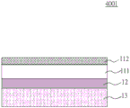
In addition, the present test example mainly tests the peel strength between the first adhesive layer 12 and the first protective film 13 in a transparent conductive laminated structure 4001 (as shown in fig. 11), and tests the effect on the peel strength after heat treatment. The transparent conductive film laminated structure 4001 in example 4 was not heat-treated, the transparent conductive film laminated structure 4001 in example 5 was heat-treated at 150 ℃ for 50 minutes, the transparent conductive film laminated structure 4001 in example 6 was heat-treated at 150 ℃, 50 minutes, and 140 ℃ for 40 minutes, and the peel strength between the first adhesive layer 12 and the first protective film 13 in each test example was measured. The test results are shown in table 2:
TABLE 2
| Example 4 | Example 5 | Example 6 | |
| Peel Strength (mN/25mm) | 115 | 64 | 176 |
The results of the above test example 2 show that the peel strength of example 5 is decreased by 44% and the peel strength of example 6 is increased by 53%, however, the peel strength between the first adhesive layer 12 and the first protective film 13 is still less than 200mN/25mm, so that the first protective film 13 still maintains the releasing ability with respect to the first adhesive layer 12.
The above examples are only for illustrating the embodiments of the present invention and illustrating the technical features of the present invention, and are not intended to limit the scope of the present invention. Any modifications or equivalent arrangements which may occur to those skilled in the art and which fall within the spirit and scope of the appended claims should be construed as broadly as the following claims.
Claims (16)
1. A transparent conductive laminate structure, comprising:
a first conductive film comprising a first surface and a second surface opposite to the first surface;
a first adhesive layer disposed on the first surface of the first conductive film; and
a protective film disposed on the first adhesive layer;
wherein the peel strength between the first adhesion layer and the first conductive film is greater than the peel strength between the first adhesion layer and the protective film.
2. The transparent conductive laminate according to claim 1, wherein the peel strength between the first adhesive layer and the first conductive film is more than 100 times the peel strength between the first adhesive layer and the protective film.
3. The transparent conductive laminate according to claim 2, wherein the peel strength between the first adhesive layer and the protective film is less than 200mN/25 mm.
4. The transparent conductive laminated structure according to claim 1, wherein the first conductive film comprises a first substrate and a first conductive layer formed on the first substrate, and the first adhesive layer is disposed between the first substrate and the protective film or between the first conductive layer and the protective film.
5. The transparent conductive laminate structure of claim 1, wherein the first conductive layer comprises a plurality of nano-metal lines.
6. The transparent conductive laminate structure of claim 1, further comprising:
a second adhesive layer disposed on the second surface of the first conductive film; and
a release film arranged on the second adhesion layer;
the peeling strength between the second adhesion layer and the first conductive film is greater than that between the second adhesion layer and the release film.
7. The transparent conductive laminated structure according to claim 6, wherein the first conductive film comprises a first substrate and a first conductive layer formed on the first substrate, the first adhesive layer is disposed between the first substrate and the protective film, and the second adhesive layer is disposed between the first conductive layer and the release film.
8. The transparent conductive laminated structure of claim 7, wherein a peel strength between the second adhesive layer and the first conductive layer is more than 100 times a peel strength between the second adhesive layer and the release film.
9. The transparent conductive laminate according to claim 8, wherein the peel strength between the second adhesive layer and the protective film is less than 200mN/25 mm.
10. A touch panel, comprising:
a first conductive film including a first substrate and a first conductive layer disposed on the first substrate;
the second conductive film is arranged below the first conductive film and comprises a second substrate and a second conductive layer arranged on the second substrate; and
the first adhesion layer is arranged between the first conductive film and the second conductive film and is contacted with the second conductive layer and the first substrate;
wherein the peel strength between the first adhesive layer and the second conductive layer is greater than 15000mN/25 mm.
11. The touch panel of claim 10, further comprising:
a protective film; and
a third adhesion layer arranged between the second substrate and the protective film;
the peeling strength between the third adhesion layer and the second substrate is greater than that between the third adhesion layer and the protective film.
12. The touch panel of claim 11, wherein the peel strength between the third adhesive layer and the second substrate is more than 100 times the peel strength between the third adhesive layer and the protective film.
13. The touch panel of claim 11, wherein the peel strength between the third adhesive layer and the protective film is less than 200mN/25 mm.
14. The touch panel of claim 11, wherein the first conductive layer and the second conductive layer each comprise a plurality of nano-metal wires.
15. The touch panel of claim 12, wherein the first conductive layer and the second conductive layer are patterned electrode layers respectively.
16. The touch panel of claim 13, further comprising an optical adhesive and a top cover layer, wherein the top cover layer is attached to the first conductive layer by the optical adhesive.
Priority Applications (3)
| Application Number | Priority Date | Filing Date | Title |
|---|---|---|---|
| CN202010521524.0A CN113778251A (en) | 2020-06-10 | 2020-06-10 | Transparent conductive laminated structure and touch panel |
| JP2020167616A JP2021194908A (en) | 2020-06-10 | 2020-10-02 | Transparent conductive laminated structure and touch panel |
| KR1020200143060A KR20210154066A (en) | 2020-06-10 | 2020-10-30 | Transparent conductive laminated structure and touch panel |
Applications Claiming Priority (1)
| Application Number | Priority Date | Filing Date | Title |
|---|---|---|---|
| CN202010521524.0A CN113778251A (en) | 2020-06-10 | 2020-06-10 | Transparent conductive laminated structure and touch panel |
Publications (1)
| Publication Number | Publication Date |
|---|---|
| CN113778251A true CN113778251A (en) | 2021-12-10 |
Family
ID=78834488
Family Applications (1)
| Application Number | Title | Priority Date | Filing Date |
|---|---|---|---|
| CN202010521524.0A Withdrawn CN113778251A (en) | 2020-06-10 | 2020-06-10 | Transparent conductive laminated structure and touch panel |
Country Status (3)
| Country | Link |
|---|---|
| JP (1) | JP2021194908A (en) |
| KR (1) | KR20210154066A (en) |
| CN (1) | CN113778251A (en) |
Families Citing this family (1)
| Publication number | Priority date | Publication date | Assignee | Title |
|---|---|---|---|---|
| JP2023154610A (en) * | 2022-04-07 | 2023-10-20 | 日東電工株式会社 | Transparent conductive film with protective film |
Family Cites Families (13)
| Publication number | Priority date | Publication date | Assignee | Title |
|---|---|---|---|---|
| JP5816591B2 (en) * | 2012-04-27 | 2015-11-18 | 信越ポリマー株式会社 | Manufacturing method of transparent wiring sheet |
| JP3182510U (en) * | 2013-01-17 | 2013-04-04 | 大量科技股▲ふん▼有限公司 | Touch panel |
| JP5860845B2 (en) * | 2013-07-09 | 2016-02-16 | 日本写真印刷株式会社 | Touch sensor and method of manufacturing touch sensor |
| US9759846B2 (en) * | 2013-09-27 | 2017-09-12 | Cam Holding Corporation | Silver nanostructure-based optical stacks and touch sensors with UV protection |
| CN103745766B (en) * | 2013-12-30 | 2017-08-25 | 南京汇金锦元光电材料有限公司 | Flexibility disappears shadow transparent conductive film and touch-screen |
| WO2016002279A1 (en) * | 2014-06-30 | 2016-01-07 | 富士フイルム株式会社 | Touch panel and method for manufacturing same |
| JP2016045841A (en) * | 2014-08-26 | 2016-04-04 | アルプス電気株式会社 | Input device and manufacturing method of the same |
| JP6770799B2 (en) * | 2014-11-28 | 2020-10-21 | 三星エスディアイ株式会社Samsung SDI Co., Ltd. | Adhesive for optical film, adhesive layer for optical film, optical member and image display device |
| US9530534B2 (en) * | 2015-04-03 | 2016-12-27 | C3Nano Inc. | Transparent conductive film |
| JP2016207200A (en) * | 2015-04-20 | 2016-12-08 | ホシデン株式会社 | Touch panel and manufacturing method thereof |
| CN107533253B (en) * | 2015-05-13 | 2021-02-02 | 柯尼卡美能达株式会社 | Liquid crystal display device with touch panel and manufacturing method thereof |
| JP2017198878A (en) * | 2016-04-28 | 2017-11-02 | 日立化成株式会社 | Photosensitive conductive film and conductive pattern comprising the same, conductive pattern substrate, and method for producing touch panel sensor |
| EP3526801B1 (en) * | 2016-10-14 | 2022-12-07 | C3Nano Inc. | Stabilized sparse metal conductive films and solutions for delivery of stabilizing compounds |
-
2020
- 2020-06-10 CN CN202010521524.0A patent/CN113778251A/en not_active Withdrawn
- 2020-10-02 JP JP2020167616A patent/JP2021194908A/en active Pending
- 2020-10-30 KR KR1020200143060A patent/KR20210154066A/en not_active Ceased
Also Published As
| Publication number | Publication date |
|---|---|
| KR20210154066A (en) | 2021-12-20 |
| JP2021194908A (en) | 2021-12-27 |
Similar Documents
| Publication | Publication Date | Title |
|---|---|---|
| US11094756B2 (en) | OLED integrated digitizer and method of preparing the same | |
| US8115751B2 (en) | Capacitive touch sensing assembly | |
| JP2007508639A (en) | Patterned conductor touch screen with improved optical properties | |
| CN103744571A (en) | Ultrathin touch sensor and manufacturing method thereof | |
| EP3667469B1 (en) | Input device manufacturing method and input device | |
| US20190196549A1 (en) | Touch sensor, touch panel and method for manufacturing the same | |
| US20110115723A1 (en) | Flat-surface resistive touch panel | |
| EP2558904B1 (en) | Internal stack-up structure of touch panel and method for producing the same | |
| KR101103535B1 (en) | Capacitive touch panel having a transparent conductive film deposited directly on the cover layer and a manufacturing method thereof | |
| CN113778251A (en) | Transparent conductive laminated structure and touch panel | |
| TW201511943A (en) | Capacitive touch panel | |
| CN212208254U (en) | Transparent conductive laminated structure and touch panel | |
| KR101537161B1 (en) | Surface panel with detection function and method for manufacturing thereof | |
| US20140293146A1 (en) | Conductive film, method for manufacturing the same, and touch screen including the same | |
| TWI486859B (en) | Capacitive touch panel structure | |
| TW201510835A (en) | Capacitive touch panel | |
| JP2013222590A (en) | Conductive pattern formation substrate and manufacturing method thereof | |
| TWI744964B (en) | Transparent conductive laminated structure and touch panel | |
| CN203366779U (en) | Conductive film | |
| US8987625B2 (en) | Capacitive touch panel structure | |
| TWM429931U (en) | Electromagnetic shielding structure of transparent capacitive touch panel | |
| US11029772B1 (en) | Transparent conductive laminated structure including a first conductive film and first adhesive layer disposed on the first conductive film and touch panel | |
| JP3159486U (en) | Conductive laminate | |
| CN202142047U (en) | capacitive touch panel | |
| TWI475458B (en) | Panel with sensing structure and manufacturing method thereof |
Legal Events
| Date | Code | Title | Description |
|---|---|---|---|
| PB01 | Publication | ||
| PB01 | Publication | ||
| SE01 | Entry into force of request for substantive examination | ||
| SE01 | Entry into force of request for substantive examination | ||
| WW01 | Invention patent application withdrawn after publication | ||
| WW01 | Invention patent application withdrawn after publication |
Application publication date: 20211210 |