Narrow-bandgap semiconductor transistor and preparation method thereof
Technical Field
The present invention relates to a semiconductor device and a method for fabricating the same, and more particularly, to a carbon nanotube field effect transistor having a buried oxide layer and a method for fabricating the same.
Background
As semiconductor integrated circuit technology continues to scale down to sub-3 nm technology nodes, silicon-based integrated circuits are likely to reach the limits of silicon materials and physical quantum mechanics. With the continued development of the electronic industry, there is a strong need to find new materials with more potential and advantages to extend silicon materials, and break through the limits of moore's law. Carbon Nanotubes (CNTs) have high carrier mobility and long mean free path, nano-scale tube diameter, and can be used to build faster, lower power consumption, smaller-sized nano-field effect transistors, and thus Carbon Nanotube (CNTs) electrons are considered as one of the future information technologies that have the potential to extend silicon-based CMOS devices and continue to support moore's law.
For low-dimensional materials such as carbon nanotubes, graphene and black phosphorus, the forbidden band width is generally smaller than that of silicon, wherein the typical band gap of the carbon nanotubes is about 0.8eV, the band gap of the corresponding silicon is about 1.12eV, and the leakage end barrier width in an off state is greatly compressed due to the narrow band gap, so that larger tunneling current is generated, and the static energy consumption is increased. The off-state tunneling effect of the narrow-bandgap channel transistor is more obvious than that of a silicon-based transistor, a stable doping means is absent for a high-performance low-dimensional channel material at present, and metal is adopted as a source electrode and a drain electrode to be contacted in a mainstream method, so that the Schottky barrier near a channel partial drain end is too thin due to too strong electric field at the drain end, and a serious reverse tunneling effect is caused. And no ion implantation and doping are carried out in the preparation process of the transistor, so that the light doped source drain (LDD) of the silicon-based transistor can not be realized to finely regulate the distribution of the doping concentration of a drain end on the space, and the negative effects such as short channel effect, junction leakage current, parasitic current and the like are reduced.
The existing solution to this problem is to use an asymmetric gate stack structure or a feedback gate structure, and the asymmetric gate structure is generally based on a bottom gate and has a complex process, which is not favorable for the size reduction and scale preparation of devices. The feedback gate is connected to the position near the channel leakage end, and the feedback gate is in short circuit with the metal electrode at the leakage end, so that a channel potential barrier at the leakage end is clamped by the potential at the leakage end, a larger potential barrier width is kept, the reverse tunneling current is greatly inhibited by the larger potential barrier width, the static power consumption is reduced, and the switching ratio is improved. In the feedback gate transistor, the introduction of the secondary gate also needs to increase the area of the device, and limits the size reduction of the device.
Therefore, there is a need to design a device structure capable of optimizing the band distribution of a semiconductor transistor, suppressing off-state current and static power consumption, and compatible with an industrialized semiconductor process, and capable of realizing large-scale integrated manufacturing.
Disclosure of Invention
Aiming at the problems in the prior art, the invention provides a semiconductor transistor with a buried oxide layer and a preparation method thereof, and the technical scheme is as follows:
a long channel narrow bandgap semiconductor transistor, wherein the long channel has a typical channel length greater than 100nm, comprises a substrate having a high- κ buried oxide layer on said substrate, a narrow bandgap semiconductor channel layer on said high- κ buried oxide layer, a gate structure on said narrow bandgap semiconductor channel layer, said gate structure comprising sidewalls and a gate dielectric layer and a gate electrode between said sidewalls, a source electrode and a drain electrode on both sides of said gate structure.
Preferably, the high- κ buried oxide layer is selected from hafnium oxide (HfO)2) Alumina (Al)2O3) Zirconium oxide (ZrO)2) Yttrium oxide (Y)2O3) Lanthanum oxide (La)2O3) Or titanium oxide (TiO)2)。
Preferably, the typical band gap of the above-mentioned narrow band gap semiconductor channel layer is less than 1ev, preferably from carbon nanotubes, graphene, germanium, two-dimensional materials such as molybdenum disulfide, tungsten disulfide, black phosphorus, or various combinations of these materials on the same plane or on different stacks.
Preferably, the narrow bandgap semiconductor channel layer has a width equal to a width of the gate structure, and the source and drain are in contact with sides of the narrow bandgap semiconductor channel layer.
Preferably, the narrow bandgap semiconductor channel layer has a width exceeding the width of the gate structure, and the source and the drain cover the exceeding portion of the narrow bandgap semiconductor channel layer to form a source-drain contact.
Preferably, the substrate is selected from a hard insulating material such as silicon oxide, quartz, glass, and alumina, or a high temperature resistant flexible insulating material such as PET (polyethylene terephthalate), PEN (polyethylene naphthalate), and polyimide, and is preferably a silicon substrate.
Preferably, the source and the drain are selected from any one of titanium nitride (TiN), tantalum nitride (TaN), aluminum (Al), copper (Cu), cobalt (Co), molybdenum (Mo), tungsten (W), palladium (Pd), platinum (Pt), scandium (Sc), yttrium (Y), and erbium (Er), or alloys or stacked combinations of different types of the above materials.
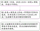
In another aspect of the present invention, a method for manufacturing the long-channel narrow-bandgap semiconductor transistor is provided, which includes the following steps:
s1: providing a substrate, growing a high-kappa buried oxide layer on the substrate, and flattening the high-kappa buried oxide layer;
s2, forming a narrow band gap semiconductor channel layer on the high-kappa buried oxide layer, and forming a gate structure comprising a gate dielectric layer and a gate on the narrow band gap semiconductor channel layer by adopting a photoetching process and a deposition process;
and S3, removing the narrow bandgap semiconductor channel layer on both sides of the gate structure by using the gate structure as a pattern, and then depositing a source electrode and a drain electrode on both sides of the gate structure.
Preferably, wherein the narrow bandgap semiconductor channel layer on both sides of the gate structure is not removed in step S3, a source and a drain are formed directly on both sides of the gate structure to cover the narrow bandgap semiconductor channel layer.
Preferably, the high- κ buried oxide layer is hafnium oxide (HfO)2) Alumina (Al)2O3) Zirconium oxide (ZrO)2) Yttrium oxide (Y)2O3) Lanthanum oxide (La)2O3) Or titanium oxide (TiO)2)。
Preferably, the typical band gap of the above-mentioned narrow band gap semiconductor channel layer is less than 1ev, preferably from carbon nanotubes, graphene, germanium, two-dimensional materials such as molybdenum disulfide, tungsten disulfide, black phosphorus, or various combinations of these materials on the same plane or on different stacks.
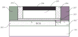
In another aspect of the present invention, a short channel narrow bandgap semiconductor transistor is provided, wherein the short channel is typically less than 100nm in length in a semiconductor channel, having a substrate with a heterogeneous buried oxide layer on the substrate, a narrow bandgap semiconductor channel layer on the heterogeneous buried oxide layer, a gate structure on the narrow bandgap semiconductor channel layer, the gate structure including sidewalls and a gate dielectric and a gate electrode between the sidewalls, a source electrode and a drain electrode on either side of the gate structure, wherein,
the heterogeneous buried oxide layer comprises a low-kappa buried oxide layer with the width of L1 and a high-kappa buried oxide layer with the width of L2, wherein L1>L2, the high- κ buried oxide layer being on the drain side and having an overlap width L with the narrow bandgap semiconductor channel layerov。
Preferably, the low- κ buried oxide layer is silicon dioxide (SiO)2) The high-k buried oxide layer (101) is hafnium oxide (HfO)2) Alumina (Al)2O3) Zirconium oxide (ZrO)2) Yttrium oxide (Y)2O3) Lanthanum oxide (La)2O3) Or titanium oxide (TiO)2)。
Preferably, the typical band gap of the above-mentioned narrow band gap semiconductor channel layer is less than 1ev, and may be selected from carbon nanotube, graphene, germanium, two-dimensional material such as molybdenum disulfide, tungsten disulfide, black phosphorus, or various combinations of these materials on the same plane or different stacked layers.
Preferably, the narrow bandgap semiconductor channel layer has a width equal to a width of the gate structure, and the source and drain electrodes are in contact with side surfaces of the low dimensional semiconductor channel layer.
Preferably, the narrow bandgap semiconductor channel layer has a width that exceeds the width of the gate structure, and the source and drain electrodes form contacts overlying the excess portion of the narrow bandgap semiconductor channel layer.
Preferably, the substrate is a hard insulating material selected from silicon oxide, quartz, glass, alumina, and the like, or a high temperature resistant flexible insulating material selected from PET (polyethylene terephthalate), PEN (polyethylene naphthalate), polyimide, and the like, and is preferably a silicon substrate.
Preferably, the source and the drain are selected from any one of titanium nitride (TiN), tantalum nitride (TaN), aluminum (Al), copper (Cu), cobalt (Co), molybdenum (Mo), tungsten (W), palladium (Pd), platinum (Pt), scandium (Sc), yttrium (Y), and erbium (Er), or alloys or stacked combinations of different types of the above materials.
In another aspect of the present invention, a method for manufacturing the short-channel narrow bandgap semiconductor transistor is further provided, which includes the following steps:
s1: providing a substrate, growing a low-k buried oxide layer on the substrate, and forming a high-k buried oxide layer pattern through a photoetching process;
s2, etching the low-kappa oxygen burying layer corresponding to the high-kappa oxygen burying layer pattern to form a low-kappa oxygen burying layer with the width of L1, further depositing a high-kappa oxygen burying layer with the width of L2 in the groove formed after etching, and then carrying out chemical mechanical polishing to form a heterogeneous oxygen burying layer;
s3, forming a narrow band gap semiconductor channel layer on the heterogeneous buried oxide layer, and forming a gate structure comprising a gate dielectric layer and a gate electrode on the narrow band gap semiconductor channel layer by adopting a photoetching process and a deposition process;
and S4, removing the narrow-bandgap semiconductor channel layer on two sides of the gate structure by taking the gate structure as a pattern, and then depositing a source electrode and a drain electrode on two sides of the gate structure.
Preferably, the high- κ buried oxide layer is hafnium oxide (HfO)2) Alumina (Al)2O3) Zirconium oxide (ZrO)2) Yttrium oxide (Y)2O3) Lanthanum oxide (La)2O3) Or titanium oxide (TiO)2)。
Preferably, the typical band gap of the above-mentioned narrow band gap semiconductor channel layer is less than 1ev, preferably from carbon nanotubes, graphene, germanium, two-dimensional materials such as molybdenum disulfide, tungsten disulfide, black phosphorus, or various combinations of these materials on the same plane or on different stacks.
Preferably, wherein the narrow bandgap semiconductor channel layer on both sides of the gate structure may not be removed in step S4, a source electrode and a drain electrode covering the narrow bandgap semiconductor channel layer may be directly formed on both sides of the gate structure.
According to the invention, through the design of the high-kappa buried oxide layer, for a long-channel transistor, the high-kappa buried oxide layer can realize strong electrostatic coupling between the drain electrode and the drain end of the channel, so that the drain end potential clamps the thickness of a Schottky barrier, and for a short-channel transistor, the heterogeneous buried oxide layer is adopted to reduce the short-channel effect and enhance the electrostatic coupling between the drain electrode and the drain end of the channel, thereby solving the problem of static power consumption caused by off-state tunneling current.
Drawings
The above and other objects, features and advantages of the present invention will become more apparent by describing the technical solution thereof with reference to the accompanying drawings, in which:
FIG. 1 is a schematic diagram of a long channel narrow bandgap semiconductor transistor in accordance with the present invention;
FIG. 2 is a flow chart of the process for fabricating a long channel narrow bandgap semiconductor transistor in accordance with the present invention;
FIG. 3 is a graph of the transfer characteristics of a long channel narrow bandgap semiconductor transistor of the present invention;
FIG. 4 is an off-state band diagram of the long channel narrow bandgap semiconductor transistor;
FIG. 5 is a schematic diagram of a short channel narrow bandgap semiconductor transistor in accordance with the present invention;
FIG. 6 is a comparison of various performance indexes of a 50nm gate length transistor based on different buried oxide layers according to the present invention;
FIG. 7 is a flow chart of the fabrication of a short channel narrow bandgap semiconductor transistor in accordance with the present invention;
Detailed Description
Embodiments of the present invention will be described in detail below with reference to the accompanying drawings. Like elements in the drawings are represented by like reference numerals, and parts of the drawings are not drawn to scale. In addition, certain well known components may not be shown. For simplicity, the semiconductor structure obtained after several steps can be described in one figure.
It will be understood that when a layer or region is referred to as being "on" or "over" another layer or region in describing the structure of the device, it can be directly on the other layer or region or intervening layers or regions may also be present. And, if the device is turned over, that layer, region, or regions would be "under" or "beneath" another layer, region, or regions.
If for the purpose of describing the situation directly above another layer, another region, the expression "a directly above B" or "a above and adjacent to B" will be used herein. In the present application, "a is directly in B" means that a is in B and a and B are directly adjacent, rather than a being in a doped region formed in B.
The present invention is described in detail below with reference to fig. 1 to 7.
Example one
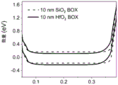
The long channel narrow bandgap semiconductor transistor of this embodiment is shown in fig. 1, and has a silicon substrate 101 with hafnium oxide (HfO) thereon2) The high- κ buried oxide layer 102, and in other embodiments, the high- κ buried oxide layer 102 may also be selected from alumina (Al)2O3) Zirconium oxide (ZrO)2) Yttrium oxide (Y)2O3) Lanthanum oxide (La)2O3) Or titanium oxide (TiO)2) And the like. In hafnium oxide (HfO)2) The high- κ buried oxide layer 102 has a carbon nanotube channel layer 103 thereon. In other embodiments, the channel layer may be selected from graphene, germanium, two-dimensional materials such as molybdenum disulfide, tungsten disulfide, black phosphorus, or various combinations of these materials on the same plane or on different stacks. In the carbon nanotube channel layer102 has a gate structure including two sidewalls 104 and 104', a gate dielectric layer 105 between the sidewalls and a gate 106 thereon, and a source 107 and a drain 108 on two sides of the gate structure. Fig. 2 is a graph of the transfer characteristics of this example, from which it can be seen that the off-state current of a transistor device employing a high- κ buried oxide layer is reduced by an order of magnitude relative to a conventional low- κ buried oxide layer. Fig. 3 is a simulated off-state band diagram of the device of this embodiment, from which it can be seen that the transistor device employing the high- κ buried oxide layer can improve the gate efficiency and enhance the electrostatic coupling of the drain and drain terminal energy bands, clamping the drain terminal schottky barrier thickness to some extent.
In the present embodiment, the carbon nanotube channel layer 103 has the same width as the gate structure described above, and the source electrode 107 and the drain electrode 108 are brought into contact with the side surfaces of the carbon nanotube channel layer 103. In another embodiment, the width of the carbon nanotube channel layer 103 exceeds the width of the gate structure, and the source 107 and the drain 108 respectively cover the excess portions of the carbon nanotube channel layer 103 to form source and drain contacts.
In this embodiment, the source 107 and the drain 108 are each palladium (Pd), and in other embodiments, the source 106 and the drain 107 are each selected from titanium nitride (TiN), tantalum nitride (TaN), aluminum (Al), copper (Cu), cobalt (Co), molybdenum (Mo), tungsten (W), scandium (Sc), platinum (Pt), scandium (Sc), yttrium (Y), and erbium (Er), or a combination of different types of alloys or stacks thereof.
Fig. 4 is a flowchart of a method for manufacturing the long-channel narrow-bandgap semiconductor transistor, which mainly includes the following steps:
s1: providing a silicon substrate 101, growing a hafnium oxide buried oxide layer 102 on the silicon substrate, and flattening; in other embodiments, the buried oxide layer may also be made of aluminum oxide (Al)2O3) Zirconium oxide (ZrO)2) Yttrium oxide (Y)2O3) Lanthanum oxide (La)2O3) Titanium oxide (TiO)2)。
S2, forming a carbon nanotube channel layer 103 on the hafnium oxide buried oxide layer 102, and forming a gate structure including a gate dielectric layer 105 and a gate electrode 106 thereon by using a conventional photolithography process and a deposition process in the art; in other embodiments, the semiconductor channel layer may employ a semiconductor material with a bandgap of less than 1ev, such as graphene, germanium, two-dimensional materials such as molybdenum disulfide, tungsten disulfide, black phosphorus, or various combinations of these materials on the same plane or on different stacks.
And S3, removing the carbon nanotube channel layer on two sides of the gate structure by taking the gate structure as a pattern, and then depositing metal Pd on two sides of the gate structure to form a source electrode 107 and a drain electrode 108.
In other embodiments, the source electrode 107 and the drain electrode 108 covering the carbon nanotube channel layer may be directly formed on both sides of the gate structure without removing the carbon nanotube channel layer on both sides of the gate structure in step S3.
Example two
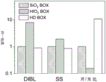
The short channel narrow bandgap semiconductor transistor of this embodiment is shown in fig. 5 and has a silicon substrate 201 with a heteroburied oxide layer thereon having a low-k silicon dioxide buried oxide layer 202 with a width of L1 and a high-k hafnium dioxide buried oxide layer 202' with a width of L2, wherein L1>L2. A carbon nanotube channel layer 203 is formed on the heterogeneous buried oxide layer, a gate structure is formed thereon, the gate structure comprises two side walls 204 and 204 ', a gate dielectric layer 205 is formed between the side walls and a gate 206 is formed thereon, a metal Pd source 207 and a drain 208 are formed on the two sides of the gate structure, a high- κ hafnium oxide buried oxide layer 202' is formed on the drain 208 and has an overlap width L with the carbon nanotube channel layer 203ovAnd the optimized current switching ratio can be realized by adjusting the overlapping width so as to ensure that the static power consumption design requirement of the transistor is met. FIG. 6 is a comparison of various simulated performance indicators of 50nm gate length transistors based on different buried oxide layers, including source induced barrier lowering (DIBL), sub-threshold swing (SS) and on/off ratio (on/off ratio) according to the present embodiment. With SiO2HfO compared to buried oxide devices2The off-state performance of the buried oxide layer device is poor and the short channel effect is obvious, namely DIBL is 222mV/V, SS is 177mV/dec and on/off ratio is 8.9 multiplied by 103. For a hetero-buried oxide layer device, DIBL is 25mV/V and SS is 80mV/dec, while the on-off ratio is compared to SiO2The buried oxide layer device is improved by one order of magnitude. The aboveThe results prove the advantages and application potential of the heterogeneous buried oxide layer structure in the short-channel device.
In other embodiments, the high- κ buried oxide layer 202' may also be selected from alumina (Al)2O3) Zirconium oxide (ZrO)2) Yttrium oxide (Y)2O3) Lanthanum oxide (La)2O3) Or titanium oxide (TiO)2) And the like. Wherein the typical band gap of the semiconductor channel layer is less than 1ev, can be selected from carbon nanotubes, graphene, germanium, two-dimensional materials such as molybdenum disulfide, tungsten disulfide, black phosphorus, or various combinations of these materials on the same plane or on different stacks.
In the present embodiment, the carbon nanotube channel layer 203 has the same width as the gate structure described above, and the source electrode 207 and the drain electrode 208 are in contact with the side surfaces of the carbon nanotube channel layer 203. In another embodiment, the width of the carbon nanotube channel layer 203 exceeds the width of the gate structure, and the source electrode 207 and the drain electrode 208 cover the excess portion of the carbon nanotube channel layer 203 to form a contact.
In other embodiments, the source 206 and the drain 207 may be selected from any one of titanium nitride (TiN), tantalum nitride (TaN), aluminum (Al), copper (Cu), cobalt (Co), molybdenum (Mo), tungsten (W), scandium (Sc), platinum (Pt), scandium (Sc), yttrium (Y), and erbium (Er), or a different alloy or stacked combination thereof.
Fig. 6 is a method of fabricating a short channel narrow bandgap semiconductor transistor comprising the steps of:
s1: providing a substrate 201, growing a low-k silicon dioxide buried oxide layer 202 thereon, and forming a high-k buried oxide layer pattern by a photolithography process conventional in the art;
s2, etching the low-kappa silicon dioxide oxygen burying layer corresponding to the high-kappa oxygen burying layer pattern to form a low-kappa silicon dioxide oxygen burying layer 202 with the width of L1, further depositing a high-kappa hafnium dioxide oxygen burying layer 202' with the width of L2 in a groove formed after etching, and then carrying out chemical mechanical polishing to form a heterogeneous oxygen burying layer; in other embodiments, the high- κ buried oxide layer may also be made of aluminum oxide (Al)2O3) Zirconium oxide (ZrO)2) Yttrium oxide (Y)2O3) Oxygen, oxygenLanthanum (La)2O3) Or titanium oxide (TiO)2)。
S3, forming a carbon nanotube channel layer 203 on the heterogeneous buried oxide layer, and forming a gate structure comprising a gate dielectric layer 205 and a gate electrode 206 thereon by using a conventional photoetching process and a deposition process in the field;
s4, removing the carbon nanotube channel layer on both sides of the gate structure using the gate structure as a pattern, and then depositing the source electrode 207 and the drain electrode 208 on both sides of the gate structure. In another embodiment, the source electrode 207 and the drain electrode 208 covering the carbon nanotube channel layer may be directly formed on both sides of the gate structure without removing the carbon nanotube channel layer on both sides of the gate structure.
In other embodiments, other narrow bandgap semiconductors, such as germanium, graphene, two-dimensional materials such as molybdenum disulfide, tungsten disulfide, black phosphorus, or various combinations of these materials on the same plane or on different stacks, with typical bandgaps less than 1ev, may be employed.
The semiconductor transistor structure extends the overlapping width between a semiconductor channel of the transistor and a high-kappa gate medium by adjusting the thickness of the low-kappa side wall between a gate electrode and a source-drain electrode of the transistor, increases a part of channel area regulated and controlled by a drain electrode, and further increases the width of a drain potential barrier, thereby solving the problem of static power consumption caused by off-state tunneling current.
Although the invention has been described in detail hereinabove with respect to specific embodiments thereof, it will be apparent to those skilled in the art that modifications and improvements can be made thereto without departing from the scope of the invention. Accordingly, such modifications and improvements are intended to be within the scope of the invention as claimed.