CN113741154A - Method for measuring alignment deviation, semiconductor device and method for manufacturing the same - Google Patents
Method for measuring alignment deviation, semiconductor device and method for manufacturing the same Download PDFInfo
- Publication number
- CN113741154A CN113741154A CN202110975123.7A CN202110975123A CN113741154A CN 113741154 A CN113741154 A CN 113741154A CN 202110975123 A CN202110975123 A CN 202110975123A CN 113741154 A CN113741154 A CN 113741154A
- Authority
- CN
- China
- Prior art keywords
- pattern
- patterns
- preset
- distance
- adjacent
- Prior art date
- Legal status (The legal status is an assumption and is not a legal conclusion. Google has not performed a legal analysis and makes no representation as to the accuracy of the status listed.)
- Pending
Links
Images


Classifications
-
- G—PHYSICS
- G03—PHOTOGRAPHY; CINEMATOGRAPHY; ANALOGOUS TECHNIQUES USING WAVES OTHER THAN OPTICAL WAVES; ELECTROGRAPHY; HOLOGRAPHY
- G03F—PHOTOMECHANICAL PRODUCTION OF TEXTURED OR PATTERNED SURFACES, e.g. FOR PRINTING, FOR PROCESSING OF SEMICONDUCTOR DEVICES; MATERIALS THEREFOR; ORIGINALS THEREFOR; APPARATUS SPECIALLY ADAPTED THEREFOR
- G03F7/00—Photomechanical, e.g. photolithographic, production of textured or patterned surfaces, e.g. printing surfaces; Materials therefor, e.g. comprising photoresists; Apparatus specially adapted therefor
- G03F7/70—Microphotolithographic exposure; Apparatus therefor
- G03F7/70483—Information management; Active and passive control; Testing; Wafer monitoring, e.g. pattern monitoring
- G03F7/70605—Workpiece metrology
- G03F7/70616—Monitoring the printed patterns
- G03F7/70633—Overlay, i.e. relative alignment between patterns printed by separate exposures in different layers, or in the same layer in multiple exposures or stitching
-
- G—PHYSICS
- G03—PHOTOGRAPHY; CINEMATOGRAPHY; ANALOGOUS TECHNIQUES USING WAVES OTHER THAN OPTICAL WAVES; ELECTROGRAPHY; HOLOGRAPHY
- G03F—PHOTOMECHANICAL PRODUCTION OF TEXTURED OR PATTERNED SURFACES, e.g. FOR PRINTING, FOR PROCESSING OF SEMICONDUCTOR DEVICES; MATERIALS THEREFOR; ORIGINALS THEREFOR; APPARATUS SPECIALLY ADAPTED THEREFOR
- G03F9/00—Registration or positioning of originals, masks, frames, photographic sheets or textured or patterned surfaces, e.g. automatically
- G03F9/70—Registration or positioning of originals, masks, frames, photographic sheets or textured or patterned surfaces, e.g. automatically for microlithography
- G03F9/7073—Alignment marks and their environment
- G03F9/708—Mark formation
-
- H—ELECTRICITY
- H10—SEMICONDUCTOR DEVICES; ELECTRIC SOLID-STATE DEVICES NOT OTHERWISE PROVIDED FOR
- H10P—GENERIC PROCESSES OR APPARATUS FOR THE MANUFACTURE OR TREATMENT OF DEVICES COVERED BY CLASS H10
- H10P72/00—Handling or holding of wafers, substrates or devices during manufacture or treatment thereof
- H10P72/50—Handling or holding of wafers, substrates or devices during manufacture or treatment thereof for positioning, orientation or alignment
- H10P72/57—Mask-wafer alignment
Landscapes
- Physics & Mathematics (AREA)
- General Physics & Mathematics (AREA)
- Exposure And Positioning Against Photoresist Photosensitive Materials (AREA)
Abstract
本公开实施例公开了一种对位偏差的量测方法、半导体器件及其制备方法,所述量测方法包括:在基底的边缘区中形成与基底的核心区中的第一图案的尺寸相同的第二图案;其中,第一图案和第二图案沿第一方向并列排布且具有第一预设距离,第一方向平行于所述基底;在边缘区中形成与基底的核心区中的第三图案的尺寸相同的第四图案;其中,第三图案和第四图案沿第一方向并列排布且具有第二预设距离,第二图案与第四图案沿所述第一方向错开;第一图案与所第三图案沿第一方向对应重叠;确定第二图案与第四图案在第一方向的偏移距离;根据偏移距离、第一预设距离和第二预设距离,确定第一图案与第三图案的对位偏差。

Embodiments of the present disclosure disclose a method for measuring alignment deviation, a semiconductor device, and a method for fabricating the same. The measuring method includes: forming a first pattern in an edge region of a substrate with the same size as a first pattern in a core region of the substrate The second pattern; wherein, the first pattern and the second pattern are arranged side by side along a first direction and have a first preset distance, and the first direction is parallel to the substrate; formed in the edge area and the core area of the substrate The third pattern has the same size as a fourth pattern; wherein the third pattern and the fourth pattern are arranged side by side along the first direction and have a second preset distance, and the second pattern and the fourth pattern are staggered along the first direction; The first pattern and the third pattern are correspondingly overlapped along the first direction; the offset distance between the second pattern and the fourth pattern in the first direction is determined; according to the offset distance, the first preset distance and the second preset distance, determine The misalignment of the first pattern and the third pattern.
Description
技术领域technical field
本公开实施例涉及半导体技术领域,特别涉及一种对位偏差的量测方法、半导体器件及其制备方法。Embodiments of the present disclosure relate to the technical field of semiconductors, and in particular, to a method for measuring alignment deviation, a semiconductor device, and a method for fabricating the same.
背景技术Background technique
光刻,是半导体芯片制造过程中的一道重要的工序,用于把掩膜版上的精细图形通过光线的曝光印制到晶圆上。随着半导体制造技术的飞速发展,器件集成度越来越高,而半导体器件的特征尺寸不断的缩小,从而对光刻工艺提出了越来越高的要求。Lithography is an important process in the semiconductor chip manufacturing process, which is used to print the fine patterns on the mask onto the wafer through light exposure. With the rapid development of semiconductor manufacturing technology, the integration of devices is getting higher and higher, and the feature size of semiconductor devices is constantly shrinking, which puts forward higher and higher requirements for the lithography process.
光刻工艺中重要的一个环节是进行层间对准,即当前层图形与硅片上已经存在的前层图形之间的对准。通常,通过量测当前层图形与前层图形之间对位偏差(overlay),来衡量当前层图形与前层图形之间的对准精度。现有技术中关于对准精度的量测,存在许多亟需解决的问题。An important link in the lithography process is to perform interlayer alignment, that is, the alignment between the current layer pattern and the previous layer pattern that already exists on the silicon wafer. Usually, the alignment accuracy between the current layer graphics and the previous layer graphics is measured by measuring the alignment deviation (overlay) between the current layer graphics and the previous layer graphics. There are many problems that need to be solved urgently in the measurement of alignment accuracy in the prior art.
发明内容SUMMARY OF THE INVENTION
有鉴于此,本公开实施例提供一种对位偏差的量测方法、半导体器件及其制备方法。In view of this, embodiments of the present disclosure provide a method for measuring alignment deviation, a semiconductor device, and a method for fabricating the same.
根据本公开实施例的第一方面,提供一种对位偏差的量测方法,包括:According to a first aspect of the embodiments of the present disclosure, a method for measuring alignment deviation is provided, including:
在基底的边缘区中形成与基底的核心区中的第一图案的尺寸相同的第二图案;其中,所述第一图案和所述第二图案沿第一方向并列排布且具有第一预设距离,所述第一方向平行于所述基底;A second pattern having the same size as the first pattern in the core region of the substrate is formed in the edge region of the substrate; wherein the first pattern and the second pattern are arranged side by side along a first direction and have a first pre- Set a distance, the first direction is parallel to the base;
在所述边缘区中形成与所述基底的核心区中的第三图案的尺寸相同的第四图案;其中,所述第三图案和所述第四图案沿所述第一方向并列排布且具有第二预设距离,所述第二图案与所述第四图案沿所述第一方向错开;所述第一图案与所述第三图案沿所述第一方向对应重叠;A fourth pattern having the same size as the third pattern in the core region of the substrate is formed in the edge region; wherein the third pattern and the fourth pattern are arranged side by side along the first direction and having a second preset distance, the second pattern and the fourth pattern are staggered along the first direction; the first pattern and the third pattern are correspondingly overlapped along the first direction;
确定所述第二图案与所述第四图案在所述第一方向的偏移距离;determining the offset distance between the second pattern and the fourth pattern in the first direction;
根据所述偏移距离、所述第一预设距离和所述第二预设距离,确定所述第一图案与所述第三图案的对位偏差。According to the offset distance, the first preset distance and the second preset distance, the alignment deviation of the first pattern and the third pattern is determined.
在一些实施例中,所述确定所述第二图案与所述第四图案在所述第一方向的偏移距离,包括:In some embodiments, the determining an offset distance between the second pattern and the fourth pattern in the first direction includes:
获取所述第二图案的第一图像,根据所述第一图像的灰度信息确定所述第二图案的中心线;依据所述第二图案的中心线获取所述第二图案的中心线的位置坐标;Obtain a first image of the second pattern, and determine the centerline of the second pattern according to the grayscale information of the first image; obtain the centerline of the second pattern according to the centerline of the second pattern Position coordinates;
获取所述第四图案的第二图像,根据所述第二图像的灰度信息确定所述第四图案的中心线;依据所述第四图案的中心线获取所述第四图案的中心线的位置坐标;Obtain a second image of the fourth pattern, and determine the centerline of the fourth pattern according to the grayscale information of the second image; obtain the centerline of the fourth pattern according to the centerline of the fourth pattern Position coordinates;
根据所述第二图案的中心线的位置坐标和所述第四图案的中心线的位置坐标,确定所述偏移距离。The offset distance is determined according to the position coordinates of the center line of the second pattern and the position coordinates of the center line of the fourth pattern.
在一些实施例中,所述根据所述偏移距离、所述第一预设距离和所述第二预设距离,确定所述第一图案与所述第三图案的对位偏差,包括:In some embodiments, the determining the alignment deviation between the first pattern and the third pattern according to the offset distance, the first preset distance and the second preset distance includes:
获取所述第一预设距离与所述第二预设距离的第一差值信息;acquiring first difference information between the first preset distance and the second preset distance;
确定所述偏移距离与所述第一差值信息的第二差值信息,以得到所述第一图案与所述第三图案的对位偏差。Second difference information between the offset distance and the first difference information is determined to obtain the alignment deviation between the first pattern and the third pattern.
在一些实施例中,所述核心区包括沿第一方向并列排布的多个所述第一图案和多个所述第三图案,所述边缘区包括沿第一方向并列排布的多个所述第二图案和多个所述第四图案;所述第二图案与所述核心区中预设子区域内的所述第一图案一一对应设置,所述第四图案与所述核心区中所述预设子区域内的所述第三图案一一对应设置;每个所述第二图案与对应的所述第一图案之间沿第一方向具有所述第一预设距离,每个所述第四图案与对应的所述第三图案之间沿第一方向具有所述第二预设距离;In some embodiments, the core region includes a plurality of the first patterns and a plurality of the third patterns arranged side by side along a first direction, and the edge region includes a plurality of the first patterns arranged side by side along the first direction the second pattern and a plurality of the fourth patterns; the second patterns are arranged in a one-to-one correspondence with the first patterns in the preset sub-regions in the core region, and the fourth patterns are arranged with the core The third patterns in the preset sub-regions in the region are set in a one-to-one correspondence; each of the second patterns and the corresponding first pattern has the first preset distance along the first direction, There is the second preset distance along the first direction between each of the fourth patterns and the corresponding third pattern;
所述确定所述第二图案与所述第四图案在所述第一方向的偏移距离,包括:The determining the offset distance between the second pattern and the fourth pattern in the first direction includes:
确定所述多个所述第二图案在所述第一方向的对称轴的第一位置坐标;determining first position coordinates of the symmetry axis of the plurality of second patterns in the first direction;
确定所述多个所述第四图案在所述第一方向的对称轴的第二位置坐标;determining second position coordinates of the symmetry axis of the plurality of fourth patterns in the first direction;
根据所述第一位置坐标和所述第二位置坐标,确定所述第二图案与所述第四图案的偏移距离。An offset distance between the second pattern and the fourth pattern is determined according to the first position coordinate and the second position coordinate.
在一些实施例中,所述第一图案,包括:所述核心区中导电的接触柱;In some embodiments, the first pattern includes: conductive contact posts in the core region;
所述第二图案,包括:所述边缘区中的支撑柱;the second pattern comprising: support posts in the edge region;
所述第三图案,包括:所述核心区中与所述接触柱电连接的导电的第一互连线;The third pattern includes: conductive first interconnect lines in the core region that are electrically connected to the contact pillars;
所述形成第四图案,包括:所述边缘区中导电的第二互连线。The forming of the fourth pattern includes: a second conductive line in the edge region.
根据本公开实施例的第二方面,提供一种半导体器件的制备方法,包括:According to a second aspect of the embodiments of the present disclosure, a method for fabricating a semiconductor device is provided, including:
图案化处理覆盖基底核心区与边缘区的第一掩膜层,以在覆盖所述核心区的所述第一掩膜层中形成第一预设图案,并在覆盖所述边缘区的所述第一掩膜层中形成第二预设图案;其中,所述第一预设图案和所述第二预设图案沿第一方向并列排布且具有第一预设距离,所述第一方向平行于所述基底;patterning the first mask layer covering the core region and the edge region of the substrate to form a first preset pattern in the first mask layer covering the core region, and forming a first preset pattern in the first mask layer covering the edge region A second preset pattern is formed in the first mask layer; wherein, the first preset pattern and the second preset pattern are arranged side by side along a first direction and have a first preset distance, and the first direction parallel to the base;
基于所述第一预设图案和所述第二预设图案,对应在所述核心区形成第一图案,并在所述边缘区形成第二图案;Based on the first preset pattern and the second preset pattern, correspondingly forming a first pattern in the core region and forming a second pattern in the edge region;
在形成所述第一图案和所述第二图案之后,图案化处理覆盖所述核心区与边缘区的第二掩膜层,以在覆盖所述核心区的所述第二掩膜层中形成第三预设图案,并在覆盖所述边缘区的所述第二掩膜层中形成第四预设图案;其中,所述第三预设图案和所述第四预设图案沿所述第一方向并列排布且具有第二预设距离;After forming the first pattern and the second pattern, a second mask layer covering the core region and the edge region is patterned to form in the second mask layer covering the core region a third preset pattern, and a fourth preset pattern is formed in the second mask layer covering the edge region; wherein the third preset pattern and the fourth preset pattern are along the first Arranged side by side in one direction and have a second preset distance;
基于所述第三预设图案和所述第四预设图案,对应在所述核心区形成第三图案,并在所述边缘区形成第四图案;其中,所述第二图案与所述第四图案沿所述第一方向错开;所述第一图案与所述第三图案沿所述第一方向对应重叠;所述第二图案与所述第四图案,用于确定所述第一图案与所述第三图案的对位偏差。Based on the third preset pattern and the fourth preset pattern, a third pattern is correspondingly formed in the core region, and a fourth pattern is formed in the edge region; wherein the second pattern and the first Four patterns are staggered along the first direction; the first pattern and the third pattern are correspondingly overlapped along the first direction; the second pattern and the fourth pattern are used to determine the first pattern misalignment with the third pattern.
在一些实施例中,沿所述第一方向,图案化处理后的所述第二掩膜层中包括等间距排布的多个所述第三预设图案和等间距排布的多个所述第四预设图案;其中,相邻两个所述第四预设图案之间的距离,等于相邻两个所述第三预设图案之间的距离;In some embodiments, along the first direction, the patterned second mask layer includes a plurality of the third preset patterns arranged at equal intervals and a plurality of all the predetermined patterns arranged at equal intervals. the fourth preset pattern; wherein, the distance between two adjacent fourth preset patterns is equal to the distance between two adjacent third preset patterns;
沿所述第一方向,图案化处理后的所述第一掩膜层中包括等间距排布的多个所述第一预设图案和等间距排布的多个所述第二预设图案;其中,Along the first direction, the patterned first mask layer includes a plurality of the first preset patterns arranged at equal intervals and a plurality of the second preset patterns arranged at equal intervals ;in,
相邻两个所述第二预设图案之间的距离,等于相邻两个所述第一预设图案之间的距离;The distance between two adjacent second preset patterns is equal to the distance between two adjacent first preset patterns;
或者,or,
相邻两个所述第二预设图案之间的距离,等于相邻两个所述第一预设图案之间距离的2倍。The distance between two adjacent second preset patterns is equal to twice the distance between two adjacent first preset patterns.
在一些实施例中,沿所述第一方向,图案化处理后的所述第一掩膜层中包括等间距排布的多个所述第一预设图案,以及等间距排布的多个所述第二预设图案;其中,相邻两个所述第二预设图案之间的距离,等于相邻两个所述第一预设图案之间的距离;In some embodiments, along the first direction, the patterned first mask layer includes a plurality of the first preset patterns arranged at equal intervals, and a plurality of first predetermined patterns arranged at equal intervals the second preset pattern; wherein, the distance between two adjacent second preset patterns is equal to the distance between two adjacent first preset patterns;
沿所述第一方向,图案化处理后的所述第二掩膜层中包括等间距排布的多个所述第三预设图案和等间距排布的多个所述第四预设图案;其中,相邻两个所述第四预设图案之间的距离,等于相邻两个所述第三预设图案之间距离的3 倍。Along the first direction, the patterned second mask layer includes a plurality of the third preset patterns arranged at equal intervals and a plurality of the fourth predetermined patterns arranged at equal intervals ; wherein, the distance between two adjacent fourth preset patterns is equal to 3 times the distance between two adjacent third preset patterns.
根据本公开实施例的第三方面,提供一种半导体器件,包括:According to a third aspect of the embodiments of the present disclosure, there is provided a semiconductor device, comprising:
位于所述基底的边缘区的第二图案,所述第一图案和所述第二图案尺寸相同,且所述第一图案与所述第二图案沿第一方向并列排布且具有第一预设距离;其中,所述第一方向平行于所述基底;A second pattern located in the edge region of the substrate, the first pattern and the second pattern have the same size, and the first pattern and the second pattern are arranged side by side along a first direction and have a first pre Set a distance; wherein, the first direction is parallel to the base;
位于所述核心区的第三图案,所述第三图案贯穿覆盖所述基底的介质层;且所述第三图案与所述第一图案沿所述第一方向一一对应重叠布置;a third pattern located in the core region, the third pattern penetrates through the dielectric layer covering the substrate; and the third pattern and the first pattern are arranged in a one-to-one correspondence along the first direction;
位于所述边缘区的第四图案,所述第四图案贯穿所述介质层;所述第三图案和所述第四图案尺寸相同,且所述第三图案和所述第四图案沿所述第一方向并列排布且具有第二预设距离;所述第四图案与所述第二图案沿所述第一方向错开;a fourth pattern located in the edge region, the fourth pattern penetrates the dielectric layer; the third pattern and the fourth pattern have the same size, and the third pattern and the fourth pattern are along the The first direction is arranged side by side and has a second preset distance; the fourth pattern and the second pattern are staggered along the first direction;
其中,所述第二图案与所述第四图案,用于确定所述第一图案与所述第三图案的对位偏差。Wherein, the second pattern and the fourth pattern are used to determine the alignment deviation between the first pattern and the third pattern.
在一些实施例中,沿所述第一方向,所述半导体器件包括:In some embodiments, along the first direction, the semiconductor device includes:
等间距排布的多个所述第三图案和等间距排布的多个所述第四图案;其中,沿所述第一方向,相邻两个所述第四图案之间的距离,等于相邻两个所述第三图案之间的距离;A plurality of the third patterns arranged at equal intervals and a plurality of the fourth patterns arranged at equal intervals; wherein, along the first direction, the distance between two adjacent fourth patterns is equal to the distance between two adjacent third patterns;
等间距排布的多个所述第一图案和等间距排布的多个所述第二图案;其中,A plurality of the first patterns arranged at equal intervals and a plurality of the second patterns arranged at equal intervals; wherein,
相邻两个所述第二图案之间的距离,等于相邻两个所述第一图案之间的距离;The distance between two adjacent second patterns is equal to the distance between two adjacent first patterns;
或者,or,
相邻两个所述第二图案之间的距离,等于相邻两个所述第一图案之间距离的2倍。The distance between two adjacent second patterns is equal to twice the distance between two adjacent first patterns.
在一些实施例中,沿所述第一方向,所述半导体器件包括:In some embodiments, along the first direction, the semiconductor device includes:
等间距排布的多个所述第一图案和等间距排布的多个第二图案;其中,相邻两个所述第二图案之间的距离,等于相邻两个所述第一图案之间的距离;A plurality of the first patterns arranged at equal intervals and a plurality of second patterns arranged at equal intervals; wherein, the distance between two adjacent second patterns is equal to two adjacent first patterns the distance between;
等间距排布的多个所述第三图案和等间距排布的多个所述第四图案;其中,沿所述第一方向,相邻两个所述第四图案之间的距离,等于相邻两个所述第三图案之间距离的3倍。A plurality of the third patterns arranged at equal intervals and a plurality of the fourth patterns arranged at equal intervals; wherein, along the first direction, the distance between two adjacent fourth patterns is equal to 3 times the distance between two adjacent third patterns.
本公开实施例通过在边缘区形成与核心区第一图案尺寸相同的第二图案,并在核心区周围的边缘区形成与核心区第三图案尺寸相同的第四图案,且沿平行于基底的第一方向,第一图案和第二图案具有第一预设距离,第三图案和第四图案具有第二预设距离,第二图案与第四图案不重叠。如此,即使在第一图案与第三图案重叠导致无法直接量测第一图案与第三图案之间的对位偏差的情况下,由于第二图案不与第四图案重叠,进而可直接量测第二图案与第四图案在第一方向的偏移距离,并结合第一预设距离与第二预设距离,得到第一图案与第三图案之间的对位偏差,提高了第一图案与第三图案之间的对位偏差的量测准确度。In the embodiment of the present disclosure, a second pattern with the same size as the first pattern in the core region is formed in the edge region, and a fourth pattern with the same size as the third pattern in the core region is formed in the edge region around the core region, and along a direction parallel to the substrate In the first direction, the first pattern and the second pattern have a first preset distance, the third pattern and the fourth pattern have a second preset distance, and the second pattern and the fourth pattern do not overlap. In this way, even if the first pattern and the third pattern overlap so that the alignment deviation between the first pattern and the third pattern cannot be directly measured, since the second pattern does not overlap with the fourth pattern, it is possible to directly measure the alignment deviation between the first pattern and the third pattern. The offset distance between the second pattern and the fourth pattern in the first direction is combined with the first preset distance and the second preset distance to obtain the alignment deviation between the first pattern and the third pattern, which improves the first pattern The measurement accuracy of the misalignment with the third pattern.
附图说明Description of drawings
图1为根据一示例性实施例示出的一种金属导线制作方法示意图;FIG. 1 is a schematic diagram of a method for manufacturing a metal wire according to an exemplary embodiment;
图2为根据一示例性实施例示出的另一种金属导线制作方法示意图;FIG. 2 is a schematic diagram illustrating another method for fabricating metal wires according to an exemplary embodiment;
图3为根据一示例性实施例示出的一种对位偏差量测方法流程图;3 is a flowchart of a method for measuring alignment deviation according to an exemplary embodiment;
图4为根据一示例性实施例示出的一种对位偏差量测方法示意图;4 is a schematic diagram of a method for measuring alignment deviation according to an exemplary embodiment;
图5为根据一示例性实施例示出的一种图案中心线确定方法示意图;5 is a schematic diagram illustrating a method for determining a pattern center line according to an exemplary embodiment;
图6a和图6b为根据一示例性实施例示出的另一种对位偏差量测方法示意图;6a and 6b are schematic diagrams illustrating another method for measuring alignment deviation according to an exemplary embodiment;
图7为根据一示例性实施例示出的一种半导体器件的制备方法流程图;FIG. 7 is a flowchart of a method for fabricating a semiconductor device according to an exemplary embodiment;
图8a和图8b为根据一示例性实施例示出的一种半导体器件的制备方法示意图;8a and 8b are schematic diagrams illustrating a method for fabricating a semiconductor device according to an exemplary embodiment;
图9a和图9b为根据一示例性实施例示出的另一种半导体器件的制备方法示意图;FIG. 9a and FIG. 9b are schematic diagrams illustrating another method for fabricating a semiconductor device according to an exemplary embodiment;
图10为根据一示例性实施例示出的一种半导体器件的结构示意图;FIG. 10 is a schematic structural diagram of a semiconductor device according to an exemplary embodiment;
图11a、图11b、图12a、图12b为根据一示例性实施例示出的另四种半导体器件的结构示意图。11a, 11b, 12a, and 12b are schematic structural diagrams of another four types of semiconductor devices according to an exemplary embodiment.
具体实施方式Detailed ways
以下结合说明书附图及具体实施例对本公开的技术方案做进一步的详细阐述。The technical solutions of the present disclosure will be further elaborated below with reference to the accompanying drawings and specific embodiments of the description.
在本公开实施例中,术语“第一”、“第二”等是用于区别类似的对象,而不用于描述特定的顺序或先后次序。In the embodiments of the present disclosure, the terms "first", "second", etc. are used to distinguish similar objects, and are not used to describe a specific order or sequence.
在本公开实施例中,术语“A与B接触”包含A与B直接接触的情形,或者A、B两者之间还间插有其它部件而A间接地与B接触的情形。In the embodiment of the present disclosure, the term "A and B are in contact" includes the situation that A and B are in direct contact, or the situation that other components are interposed between A and B, and A is indirectly in contact with B.
在本公开实施例中,术语“层”是指包括具有厚度的区域的材料部分。层可以在下方或上方结构的整体之上延伸,或者可以具有小于下方或上方结构范围的范围。此外,层可以是厚度小于连续结构厚度的均质或非均质连续结构的区域。例如,层可位于连续结构的顶表面和底表面之间,或者层可在连续结构顶表面和底表面处的任何水平面对之间。层可以水平、垂直和/或沿倾斜表面延伸。并且,层可以包括多个子层。In embodiments of the present disclosure, the term "layer" refers to a portion of a material that includes a region having a thickness. A layer may extend over the entirety of the underlying or overlying structure, or may have an extent that is less than the extent of the underlying or overlying structure. Furthermore, a layer may be a region of a homogeneous or heterogeneous continuous structure having a thickness less than the thickness of the continuous structure. For example, the layer may be located between the top and bottom surfaces of the continuous structure, or the layer may be between any horizontal facing at the top and bottom surfaces of the continuous structure. Layers may extend horizontally, vertically and/or along inclined surfaces. Also, a layer may include multiple sub-layers.
可以理解的是,本公开中的“在……上”、“在……之上”和“在……上方”的含义应当以最宽方式被解读,以使得“在……上”不仅表示其“在”某物“上”且其间没有居间特征或层(即直接在某物上)的含义,而且还包括“在”某物“上”且其间有居间特征或层的含义。It is to be understood that the meanings of "on," "on," and "over" in this disclosure should be read in the broadest possible manner, such that "on" means not only It means "on" something "on" without intervening features or layers (ie, directly on something), but also includes the meaning of "on" something "on" with intervening features or layers.
需要说明的是,虽然本说明书按照实施方式加以描述,但并非每个实施方式仅包含一个独立的技术方案,说明书的这种叙述方式仅仅是为清楚起见,本领域技术人员应当将说明书作为一个整体,各实施方式中的技术方案也可以经适当组合,形成本领域技术人员可以理解的其它实施方式。It should be noted that although this specification is described in terms of embodiments, not every embodiment only includes an independent technical solution, and this description in the description is only for the sake of clarity, and those skilled in the art should take the description as a whole , the technical solutions in each embodiment can also be appropriately combined to form other embodiments that can be understood by those skilled in the art.
自对准双重成像(self-aligned double patterning,SADP)技术是使用深紫外线(Deep Ultraviolet Lithography,DUV)光刻设备实现40nm以下半节距工艺最普遍的方法之一。随着器件线宽的减小,光刻工艺对对准精度的要求也越来越高,实现高精度对准控制的关键在于可以精确的测量出最终实际图形(pattern)的对位偏差。Self-aligned double patterning (SADP) technology is one of the most common methods to achieve half-pitch processes below 40 nm using Deep Ultraviolet Lithography (DUV) lithography equipment. As the line width of the device decreases, the lithography process requires higher and higher alignment accuracy. The key to realizing high-precision alignment control is to accurately measure the alignment deviation of the final actual pattern.
对位偏差的一般量测方法是通过量测和当前层图形一起曝光形成的对准标记(overlay mark)的偏移量来表征的,但是由于对准标记和实际图形所处环境的差异、线宽的差异,从而会受到光刻设备像差的影响、蚀刻工艺的影响等,最终导致测得的对准标记的偏移量和实际图形的偏移量存在差异,即通过量测对准标记的偏移量不能反应实际图形的真实偏移量。The general measurement method of the alignment deviation is characterized by measuring the offset of the alignment mark (overlay mark) formed by exposure together with the current layer pattern, but due to the difference between the alignment mark and the actual pattern in the environment, the line Therefore, it will be affected by the aberration of the lithography equipment, the influence of the etching process, etc., which will eventually lead to the difference between the measured offset of the alignment mark and the offset of the actual pattern, that is, by measuring the alignment mark The offset does not reflect the actual offset of the actual graphics.
例如,相关技术中通常将对准标记形成在晶圆的切割道区域,由于切割道区域较小,对准标记的特征尺寸(线宽、线间距等)比实际图形的尺寸小得多,对对准标记位置的量测本身存在误差,对准标记之间的偏差与实际图形之间的偏差存在一定的差距。For example, in the related art, the alignment marks are usually formed on the scribe line area of the wafer. Due to the small scribe line area, the feature size (line width, line spacing, etc.) of the alignment marks is much smaller than the size of the actual pattern. There is an error in the measurement of the position of the alignment marks, and there is a certain gap between the deviation between the alignment marks and the deviation between the actual graphics.
在金属工艺制程中,对于金属互连结构,金属导线需要和下方的接触孔保持良好的对准。金属导线的制作方法通常有以下两种。In the metal processing process, for the metal interconnect structure, the metal wires need to maintain good alignment with the underlying contact holes. There are usually two methods for making metal wires.
方法一:参照图1所示,接触孔11位于衬底10中,在衬底10上沉积金属层12,再在金属层12上形成图案化的光刻胶13,通过光刻和刻蚀工艺刻蚀金属层12,以在对准接触孔11的上方形成金属导线14,然后在相邻的金属导线 14之间的空隙中填充介质层15。Method 1: Referring to FIG. 1, the
方法二:参照图2所示,接触孔21位于衬底20中,在衬底20上形成介质层22,再在介质层22上形成图案化的光刻胶23,通过光刻和刻蚀工艺刻蚀介质层22,形成暴露接触孔21的凹槽24,用金属材料填充凹槽24形成金属层 25,再通过化学机械研磨(CMP)等手段除去覆盖在介质层22上的金属层25,形成分离的金属导线26。Method 2: Referring to FIG. 2, the
由于通过量测对准标记的对位偏差来表征实际图形的对位偏差存在较大误差,一种准确获取实际图形的对位偏差的解决办法是直接量测实际图形的对位偏差,而不借助于对准标记。例如,在上述方法二中,可在接触孔21上方形成凹槽24后,且在形成金属层25之前,直接量测凹槽24与接触孔21之间的对位偏差。可以理解的是,由于金属导线26填充在凹槽24中,因此,凹槽24 与接触孔21之间的对位偏差可表征金属导线26与接触孔21之间的实际对位偏差。Since there is a large error in characterizing the alignment deviation of the actual pattern by measuring the alignment deviation of the alignment marks, a solution to accurately obtain the alignment deviation of the actual pattern is to directly measure the alignment deviation of the actual pattern without by means of alignment marks. For example, in the above-mentioned
然而,在上述方法一中,由于金属导线14是通过刻蚀金属层12形成的,导电的接触孔11在整个过程中被形成金属导线14的金属材料覆盖,无法直接量测金属导线14与接触孔11之间的对位偏差。However, in the above method 1, since the
图3是根据一示例性实施例示出的一种对位偏差的量测方法,参照图3所示,所述方法包括以下步骤:FIG. 3 shows a method for measuring alignment deviation according to an exemplary embodiment. Referring to FIG. 3 , the method includes the following steps:
S110:在基底的边缘区中形成与基底的核心区中的第一图案的尺寸相同的第二图案;其中,第一图案和第二图案沿第一方向并列排布且具有第一预设距离,第一方向平行于基底;S110 : forming a second pattern in the edge region of the substrate with the same size as the first pattern in the core region of the substrate; wherein the first pattern and the second pattern are juxtaposed along the first direction and have a first preset distance , the first direction is parallel to the base;
S120:在边缘区中形成与基底的核心区中的第三图案的尺寸相同的第四图案;其中,第三图案和第四图案沿第一方向并列排布且具有第二预设距离,第二图案与第四图案沿第一方向错开;第一图案与第三图案沿第一方向对应重叠;S120 : forming a fourth pattern in the edge region with the same size as the third pattern in the core region of the substrate; wherein the third pattern and the fourth pattern are arranged side by side along the first direction and have a second preset distance, the third pattern The second pattern and the fourth pattern are staggered along the first direction; the first pattern and the third pattern are correspondingly overlapped along the first direction;
S130:确定第二图案与第四图案在第一方向的偏移距离;S130: Determine the offset distance between the second pattern and the fourth pattern in the first direction;
S140:根据偏移距离、第一预设距离和第二预设距离,确定第一图案与第三图案的对位偏差。S140: Determine the alignment deviation between the first pattern and the third pattern according to the offset distance, the first preset distance, and the second preset distance.
示例性地,基底的核心区包括形成有功能电路结构的功能区,边缘区包括位于核心区周围不形成功能电路的区域,边缘区可以与核心区相邻或不相邻。可以理解的是,边缘区不发挥电学功能。Exemplarily, the core region of the substrate includes a functional region formed with functional circuit structures, the edge region includes a region around the core region where no functional circuit is formed, and the edge region may or may not be adjacent to the core region. It will be appreciated that the edge region does not perform an electrical function.
示例性地,第一图案与第二图案可包括位于不同区域的相同图案,且排列方向相同,可以通过同一个掩膜版同时形成。Exemplarily, the first pattern and the second pattern may include the same patterns located in different regions and arranged in the same direction, and may be formed simultaneously by the same mask.
需要说明的是,当本公开所述的图案为对称图案时,本公开中所述的图案之间的距离或者间距,可包括图案的中心或者中心线之间的距离。可以理解的是,第一图案与第二图案可包括采用一个掩膜版同时形成的同层图案,第三图案与第四图案可包括采用一个掩膜版同时形成的另一层图案。第一图案与第三图案之间沿第一方向的对位偏差,可通过第二图案与第四图案之间沿第一方向的对位偏差来表示。It should be noted that, when the patterns described in the present disclosure are symmetrical patterns, the distances or spacings between the patterns described in the present disclosure may include the distances between the centers of the patterns or the centerlines. It can be understood that the first pattern and the second pattern may include patterns of the same layer formed simultaneously using one mask, and the third pattern and the fourth pattern may include patterns of another layer formed simultaneously using one mask. The alignment deviation between the first pattern and the third pattern along the first direction can be represented by the alignment deviation between the second pattern and the fourth pattern along the first direction.
示例性地,在基底的边缘区,第二图案与第四图案沿第一方向错开,包括:沿垂直于基底的方向,第二图案与第四图案在基底上的投影完全分离,不存在重叠的部分。如此,可直接量测第二图案与第四图案的位置偏差。Exemplarily, in the edge region of the substrate, the second pattern and the fourth pattern are staggered along the first direction, including: along the direction perpendicular to the substrate, the projections of the second pattern and the fourth pattern on the substrate are completely separated, and there is no overlap part. In this way, the positional deviation between the second pattern and the fourth pattern can be directly measured.
示例性地,参照图4所示,可先采用第一掩膜版在基底上形成第一图案41 和第二图案42,再采用第二掩膜版在基底上形成第三图案43和第四图案44,并使第三图案43和第一图案41沿第一方向对准重叠,通过第一图案41与第二图案42之间的第一预设距离d1以及第三图案43与第四图案44之间的第二预设距离d2,可得到基底上第二图案和第四图案之间的预设距离,即第一预设距离d1与第二预设距离d2的差值。由于第二图案42和第四图案44沿第一方向错开,可直接量测出基底上第二图案42和第四图案44之间的偏移距离。通过第二图案42和第四图案44之间的预设距离和偏移距离,得到第一图案41和第三图案43之间的对位偏差。Exemplarily, as shown in FIG. 4 , the
需要强调的是,在一些实施例中,基底的边缘区还可包括:与第一图案结构相同的第五图案,以及与第三图案结构相同的第六图案。进一步地,第五图案与第六图案的位置关系,与第一图案与第三图案的位置关系相同。It should be emphasized that, in some embodiments, the edge region of the substrate may further include: a fifth pattern with the same structure as the first pattern, and a sixth pattern with the same structure as the third pattern. Further, the positional relationship between the fifth pattern and the sixth pattern is the same as the positional relationship between the first pattern and the third pattern.
本公开实施例通过在边缘区形成与核心区第一图案尺寸相同的第二图案,并在边缘区形成与核心区第三图案尺寸相同的第四图案,且沿平行于基底的第一方向,第一图案和第二图案具有第一预设距离,第三图案和第四图案具有第二预设距离,第二图案与第四图案不重叠。如此,即使在第一图案与第三图案重叠导致无法直接量测第一图案与第三图案之间的对位偏差的情况下,由于第二图案不与第四图案重叠,可直接量测第二图案与第四图案的在第一方向的偏移距离,并结合第一预设距离与第二预设距离,得到第一图案与第三图案之间的对位偏差,提高了第一图案与第三图案之间的对位偏差的量测准确度。In the embodiment of the present disclosure, by forming a second pattern in the edge region with the same size as the first pattern in the core region, and forming a fourth pattern in the edge region with the same size as the third pattern in the core region, along the first direction parallel to the substrate, The first pattern and the second pattern have a first predetermined distance, the third pattern and the fourth pattern have a second predetermined distance, and the second pattern and the fourth pattern do not overlap. In this way, even if the first pattern and the third pattern overlap so that the alignment deviation between the first pattern and the third pattern cannot be directly measured, since the second pattern does not overlap the fourth pattern, the first pattern can be directly measured. The offset distance between the second pattern and the fourth pattern in the first direction is combined with the first preset distance and the second preset distance to obtain the alignment deviation between the first pattern and the third pattern, which improves the first pattern The measurement accuracy of the misalignment with the third pattern.
此外,本公开实施例中通过将第二图案和第四图案设置在核心区周围的边缘区,相较于在基底的核心区或者单独设置其它区域形成第二图案和第四图案,和相较于在基底的切割道区域或者其它区域单独形成特征尺寸较小、量测误差较大的对准标记,本公开利用核心区周围原本不形成功能电路的边缘区设置第二图案和第四图案,在不额外占用基底面积且不影响核心区面积的情况下,不仅实现了对第一图案和第三图案对位偏差的量测,且减小了核心区的第一图案与第三图案的对位偏差的量测误差,提高了对位偏差量测的准确度和基底面积的利用率。In addition, in the embodiment of the present disclosure, by arranging the second pattern and the fourth pattern in the edge area around the core area, compared with forming the second pattern and the fourth pattern in the core area of the substrate or separately disposing other areas, and compared with In order to separately form alignment marks with smaller feature size and larger measurement error in the scribe line area or other areas of the substrate, the present disclosure utilizes the edge area around the core area where no functional circuit is originally formed to set the second pattern and the fourth pattern. Without additionally occupying the substrate area and without affecting the area of the core area, not only the measurement of the alignment deviation of the first pattern and the third pattern is realized, but also the alignment of the first pattern and the third pattern in the core area is reduced. The measurement error of the position deviation improves the accuracy of the position deviation measurement and the utilization rate of the substrate area.
在一些实施例中,S130可包括:In some embodiments, S130 may include:
获取第二图案的第一图像,根据第一图像的灰度信息确定第二图案的中心线;依据第二图案的中心线获取第二图案的中心线的位置坐标;acquiring the first image of the second pattern, and determining the centerline of the second pattern according to the grayscale information of the first image; acquiring the position coordinates of the centerline of the second pattern according to the centerline of the second pattern;
获取第四图案的第二图像,根据第二图像的灰度信息确定第四图案的中心线;依据第四图案的中心线获取第四图案的中心线的位置坐标;acquiring the second image of the fourth pattern, and determining the centerline of the fourth pattern according to the grayscale information of the second image; acquiring the position coordinates of the centerline of the fourth pattern according to the centerline of the fourth pattern;
根据第二图案的中心线的位置坐标和第四图案的中心线的位置坐标,确定偏移距离。The offset distance is determined according to the position coordinates of the center line of the second pattern and the position coordinates of the center line of the fourth pattern.
示例性地,可采用特征尺寸测量用扫描电子显微镜(CD-SEM)获取的基底边缘区的检测图像,从而获得第二图案的第一图像和第四图案的第二图像,并进行灰度信息分析。不同的材料成分呈现不同的灰度值,由于第二图案和第四图案与基底的材料组成不同,因此,第一图像和第二图像与基底材料的检测图像之间具有明显的区分度,可根据检测图像中的灰度信息确定第二图案和第四图案的中心线,并获取第二图案和第四图案的中心线的位置坐标。Exemplarily, the detection image of the edge region of the substrate obtained by scanning electron microscope (CD-SEM) for feature size measurement can be used to obtain the first image of the second pattern and the second image of the fourth pattern, and grayscale information can be obtained. analyze. Different material compositions present different grayscale values. Since the second pattern and the fourth pattern are different from the material composition of the substrate, the first image and the second image and the detected image of the substrate material have a clear degree of distinction, which can be easily distinguished. The center lines of the second pattern and the fourth pattern are determined according to the grayscale information in the detected image, and the position coordinates of the center lines of the second pattern and the fourth pattern are obtained.
示例性地,参照图5所示,图5示出了第一图像和第二图像的示意图,曲线A对应于第二图案42的灰度信号强度分布,曲线B对应于第四图案44的灰度信号强度分布。灰度信号强度分布曲线A中的波峰位置指示第二图案42的中心线位置,灰度信号强度分布曲线B中的波峰位置指示第四图案44的中心线位置。5 shows a schematic diagram of the first image and the second image, the curve A corresponds to the grayscale signal intensity distribution of the
参照图5所示,第二图案42和第四图案44沿平行于基底的x方向排列,根据曲线A上的波峰位置确定第二图案42的中心线L1,根据曲线B上的波峰位置确定第四图案44的中心线L3。中心线L1和中心线L3均垂直于x方向。根据中心线L1和中心线L3可以确定第二图案42和第四图案44之间的偏移距离。5, the
需要说明的是,在一些实施例中,在图案的边缘处检测到的灰度信号最强,即灰度信号强度分布曲线中波峰出现在图案的边缘处,可通过对指示图案两侧边缘位置的波峰进行拟合处理,得到指示图案中心位置的波峰。因此,图5中所示的灰度信号强度分布曲线A和灰度信号强度分布曲线B可以是经过图形处理后得到的灰度信号强度分布曲线。It should be noted that, in some embodiments, the grayscale signal detected at the edge of the pattern is the strongest, that is, the peak in the grayscale signal intensity distribution curve appears at the edge of the pattern. The peak of the pattern is fitted to obtain the peak indicating the center position of the pattern. Therefore, the grayscale signal intensity distribution curve A and the grayscale signal intensity distribution curve B shown in FIG. 5 may be grayscale signal intensity distribution curves obtained after graphic processing.
在一些实施例中,S140可包括:In some embodiments, S140 may include:
获取第一预设距离与第二预设距离的第一差值信息;acquiring first difference information between the first preset distance and the second preset distance;
确定偏移距离与第一差值信息的第二差值信息,以得到第一图案与第三图案的对位偏差。The second difference information between the offset distance and the first difference information is determined to obtain the alignment deviation between the first pattern and the third pattern.
示例性地,参照图4所示,第一图案41与第二图案42之间的第一预设距离为d1,第三图案43与第四图案44之间的第二预设距离为d2,则第一差值信息为(d1-d2),第一差值信息可表示第二图案42与第四图案44之间的预设距离。由于第二图案42与第四图案44不重叠,可直接量测出第二图案42与第四图案 44之间的偏移距离Δd,计算偏移距离Δd与第一差值信息(d1-d2)的第二差值信息ΔL,即第二差值信息ΔL等于偏移距离Δd与第一差值信息(d1-d2)之间的差值,第二差值信息ΔL即可表征第一图案41与第三图案43的对位偏差。需要说明的是,第一差值信息(d1-d2)、偏移距离Δd及第二差值信息ΔL均为表示距离的数值大小,不包含负值。Exemplarily, referring to FIG. 4 , the first preset distance between the
可以理解的是,参照图4所示,第一图案41与第三图案43分别位于第二图案42与第四图案44的左侧,当第一预设距离为d1小于第二预设距离为d2时,若偏移距离Δd大于第一差值信息(d1-d2),则说明第三图案43相对于第一图案41沿第一方向往右偏移ΔL;若偏移距离Δd小于第一差值信息(d1-d2),则说明第三图案43相对于第一图案41沿第一方向往左偏移ΔL。当第一预设距离为d1大于第二预设距离为d2时,若偏移距离Δd大于第一差值信息(d1-d2),则说明第三图案43相对于第一图案41沿第一方向往左偏移ΔL;若偏移距离Δd 小于第一差值信息(d1-d2),则说明第三图案43相对于第一图案41沿第一方向往右偏移ΔL。It can be understood that, referring to FIG. 4 , the
在一些实施例中,核心区包括沿第一方向并列排布的多个第一图案和多个第三图案,边缘区包括沿第一方向并列排布的多个第二图案和多个第四图案;第二图案与核心区中预设子区域内的第一图案一一对应设置,第四图案与核心区中预设子区域内的第三图案一一对应设置;每个第二图案与对应的第一图案之间沿第一方向具有第一预设距离,每个第四图案与对应的第三图案之间沿第一方向具有第二预设距离;In some embodiments, the core region includes a plurality of first patterns and a plurality of third patterns arranged side by side along the first direction, and the edge region includes a plurality of second patterns and a plurality of fourth patterns arranged side by side along the first direction pattern; the second pattern is set in a one-to-one correspondence with the first pattern in the preset sub-region in the core region, and the fourth pattern is set in a one-to-one correspondence with the third pattern in the preset sub-region in the core region; There is a first preset distance between the corresponding first patterns along the first direction, and each fourth pattern and the corresponding third pattern have a second preset distance along the first direction;
确定第二图案与第四图案在第一方向的偏移距离,包括:Determine the offset distance between the second pattern and the fourth pattern in the first direction, including:
确定多个第二图案在第一方向的对称轴的第一位置坐标;determining the coordinates of the first positions of the axes of symmetry of the plurality of second patterns in the first direction;
确定多个第四图案在第一方向的对称轴的第二位置坐标;determining second position coordinates of the symmetry axes of the plurality of fourth patterns in the first direction;
根据第一位置坐标和第二位置坐标,确定第二图案与第四图案的偏移距离。According to the first position coordinate and the second position coordinate, the offset distance between the second pattern and the fourth pattern is determined.
当第二图案为孔状结构或者由孔状结构得到的结构时,由于实际刻蚀工艺的均匀性问题,导致实际形成的第二图案的形状不规则或边缘不齐整,不便于确定单个第二图案的中心,量测误差较大。通过设置多个第二图案,可以取多个第二图案构成的整体的中心,并以该中心的坐标作为第一位置坐标,减小量测误差,提高量测精度。When the second pattern is a hole-like structure or a structure obtained from a hole-like structure, due to the uniformity of the actual etching process, the shape of the actually formed second pattern is irregular or the edges are irregular, which is inconvenient to determine a single second pattern. The center of the pattern has a large measurement error. By setting a plurality of second patterns, the center of the whole composed of the plurality of second patterns can be taken, and the coordinates of the center can be used as the first position coordinates, so as to reduce the measurement error and improve the measurement accuracy.
类似地,通过设置多个第四图案,也可减小量测误差,提高量测精度。Similarly, by setting a plurality of fourth patterns, the measurement error can also be reduced, and the measurement accuracy can be improved.
当包括多个第一图案和多个第二图案时,边缘区的多个第二图案与核心区的多个第一图案可以具有相同的排列方式。例如,相邻两个第一图案之间的间距与相邻两个第二图案之间的间距相同。When a plurality of first patterns and a plurality of second patterns are included, the plurality of second patterns of the edge region and the plurality of first patterns of the core region may have the same arrangement. For example, the distance between two adjacent first patterns is the same as the distance between two adjacent second patterns.
或者,第一图案和第二图案的排列方式不同但具有设定位置关系,例如,相邻两个第一图案之间的间距与相邻两个第二图案之间的间距满足一定的关系。Alternatively, the first patterns and the second patterns are arranged in different ways but have a set positional relationship. For example, the distance between two adjacent first patterns and the distance between two adjacent second patterns satisfy a certain relationship.
示例性地,第三图案与第四图案是位于不同区域的相同图案,与第一图案与第二图案的排列方向相同,可以通过同一个掩膜版同时形成。Exemplarily, the third pattern and the fourth pattern are the same pattern located in different regions, have the same arrangement direction as the first pattern and the second pattern, and can be formed simultaneously by the same mask.
当包括多个第三图案和多个第四图案时,边缘区的多个第四图案与核心区的多个第三图案可以具有相同的排列方式,例如,相邻两个第三图案之间的间距与相邻两个第四图案之间的间距相同;When a plurality of third patterns and a plurality of fourth patterns are included, the plurality of fourth patterns in the edge region and the plurality of third patterns in the core region may have the same arrangement, for example, between two adjacent third patterns The spacing is the same as the spacing between two adjacent fourth patterns;
或者,第三图案和第四图案的排列方式不同但具有设定位置关系,例如,相邻两个第三图案之间的间距与相邻两个第四图案之间的间距满足一定的关系。Alternatively, the third patterns and the fourth patterns are arranged in different ways but have a set positional relationship. For example, the distance between two adjacent third patterns and the distance between two adjacent fourth patterns satisfy a certain relationship.
示例性地,参照图6a所示,核心区包括沿x方向等间距并列排布的多个第一图案和多个第三图案,例如,包括四个第一图案41a、41b、41c和41d,以及四个第三图案43a、43b、43c和43d位于核心区中预设子区域S1内,且第三图案43a、43b、43c、43d与第一图案41a、41b、41c、41d一一对应重叠。在边缘区形成有第二图案42a和42b、以及第四图案44a和44b。在边缘区还可以形成虚拟第二图案45a和45b,与第二图案42a和42b的尺寸相同。且虚拟第二图案45a与第二图案42a之间、第二图案42a与第二图案42b之间以及第二图案42b与虚拟第二图案45b之间的间距相等,且等于相邻两个第一图案之间的间距。第四图案44a和44b可以分别与虚拟第二图案45a和45b对应重叠。6a, the core region includes a plurality of first patterns and a plurality of third patterns arranged side by side at equal intervals along the x-direction, for example, including four
第二图案42a与第一图案41b之间、第二图案42b与第一图案41c之间具有第一预设距离;第四图案44a与第三图案43a之间、第四图案44b与第三图案43d之间具有第二预设距离。There is a first preset distance between the
图6b为图6a中边缘区的局部示意图,参照图6b所示,先根据第二图案 42a的中心线L1和第二图案42b的中心线L2,确定第二图案42a和42b的对称轴L12。再根据第四图案44a的中心线L3和第四图案44b的中心线L4,确定第四图案44a和44b的对称轴L34。根据对称轴L12和对称轴L34在x方向的坐标计算差值,得到第二图案与第四图案的沿x方向的偏移距离ΔL,此时第二图案与第四图案之间的偏移距离ΔL可直接表征第一图案与第三图案之间的对位偏差。Fig. 6b is a partial schematic diagram of the edge region in Fig. 6a. Referring to Fig. 6b, first determine the symmetry axis L12 of the
或者,先通过计算第二图案42a的中心线L1的坐标与第四图案44a的中心线L3的坐标的第一差值,与第一预设距离和第二预设距离之间的第二差值,计算第一差值和第二差值得到与第四图案44a与第二图案42a之间的第一偏差。同理,通过计算第二图案42b的中心线L2的坐标与第四图案44b的中心线L4 的坐标的第三差值,计算第三差值和第二差值得到与第四图案44b与第二图案 42b之间的第二偏差。对第一偏差与第二偏差取平均值,得到第二图案与第四图案之间的偏差,即得到第一图案与第三图案之间的对位偏差。可以理解的是,通过取两组或两组以上第二图案和第四图案之间的偏差的平均值,有利于提高测得的第一图案与第三图案之间的对位偏差的精确度。Alternatively, first calculate the first difference between the coordinates of the center line L1 of the
在一些实施例中,第一图案,包括:核心区中导电的接触柱;In some embodiments, the first pattern includes: conductive contact posts in the core region;
第二图案,包括:边缘区中的支撑柱;A second pattern comprising: support posts in the edge region;
第三图案,包括:核心区中与接触柱电连接的导电的第一互连线;The third pattern includes: conductive first interconnect lines in the core area that are electrically connected to the contact pillars;
第四图案,包括:边缘区中的导电的第二互连线。The fourth pattern includes: conductive second interconnect lines in the edge region.
示例性地,位于基底核心区的第一图案可以是由导电材料填充接触孔得到的接触柱,位于边缘区的第二图案可以是与第一图案一起形成的支撑柱,接触柱与支撑柱具有相同的形状和尺寸。核心区中的接触柱与第一互连线对准重叠,边缘区中的支撑柱与第二互连线不重叠。Exemplarily, the first pattern in the core region of the substrate may be a contact pillar obtained by filling the contact hole with a conductive material, the second pattern in the edge region may be a support pillar formed together with the first pattern, and the contact pillar and the support pillar have same shape and size. The contact pillars in the core region are aligned and overlapped with the first interconnect lines, and the support pillars in the edge regions do not overlap with the second interconnect lines.
可以理解的是,接触柱与支撑柱可具有相同的结构,但支撑柱不发挥电学功能。It can be understood that the contact post and the support post may have the same structure, but the support post does not perform an electrical function.
图7为根据一示例性实施例示出的一种半导体器件的制备方法流程图。参照图7所示,所述方法包括以下步骤:FIG. 7 is a flow chart of a method for fabricating a semiconductor device according to an exemplary embodiment. Referring to Figure 7, the method includes the following steps:
S210:图案化处理覆盖基底核心区与边缘区的第一掩膜层,以在覆盖核心区的第一掩膜层中形成第一预设图案,并在覆盖边缘区的第一掩膜层中形成第二预设图案;其中,第一预设图案和第二预设图案沿第一方向并列排布且具有第一预设距离,第一方向平行于基底;S210 : patterning the first mask layer covering the core region and the edge region of the substrate to form a first preset pattern in the first mask layer covering the core region, and forming a first preset pattern in the first mask layer covering the edge region forming a second preset pattern; wherein, the first preset pattern and the second preset pattern are arranged side by side along a first direction and have a first preset distance, and the first direction is parallel to the substrate;
S220:基于第一预设图案和第二预设图案,对应在核心区形成第一图案,并在边缘区形成第二图案;S220: Based on the first preset pattern and the second preset pattern, correspondingly form the first pattern in the core region, and form the second pattern in the edge region;
S230:在形成第一图案和第二图案之后,图案化处理覆盖核心区与边缘区的第二掩膜层,以在覆盖核心区的第二掩膜层中形成第三预设图案,并在覆盖边缘区的第二掩膜层中形成第四预设图案;其中,第三预设图案和第四预设图案沿第一方向并列排布且具有第二预设距离;S230: After forming the first pattern and the second pattern, patterning the second mask layer covering the core area and the edge area to form a third preset pattern in the second mask layer covering the core area, and A fourth preset pattern is formed in the second mask layer covering the edge region; wherein the third preset pattern and the fourth preset pattern are arranged side by side along the first direction and have a second preset distance;
S240:基于第三预设图案和第四预设图案,对应在核心区形成第三图案,并在边缘区形成第四图案;其中,第二图案与第四图案沿第一方向错开;第一图案与第三图案沿所述第一方向对应重叠;第二图案与第四图案,用于确定第一图案与第三图案的对位偏差。S240: Based on the third preset pattern and the fourth preset pattern, correspondingly form a third pattern in the core region, and form a fourth pattern in the edge region; wherein the second pattern and the fourth pattern are staggered along the first direction; the first The pattern and the third pattern are correspondingly overlapped along the first direction; the second pattern and the fourth pattern are used to determine the alignment deviation between the first pattern and the third pattern.
示例性地,第一预设图案与第二预设图案具有相同的形状和尺寸,第一预设图案与第二预设图案可同时形成。第三预设图案与第四预设图案具有相同的形状和尺寸,第三预设图案与第四预设图案可同时形成。Exemplarily, the first preset pattern and the second preset pattern have the same shape and size, and the first preset pattern and the second preset pattern may be formed simultaneously. The third preset pattern and the fourth preset pattern have the same shape and size, and the third preset pattern and the fourth preset pattern can be formed simultaneously.
示例性地,第一图案为导电的接触柱,第一图案为导电的支撑柱时,则第一预设图案和第二预设图案分别为在第一掩膜层中形成的与第一图案和第二图案的形状对应的开口,通过开口在基底的核心区和边缘区形成对应的孔结构,采用导电材料填充孔结构得到接触柱和支撑柱,接触柱和支撑柱之间具有第一预设距离。类似地,可形成第三图案和第四图案的具体结构。Exemplarily, when the first pattern is a conductive contact post, and when the first pattern is a conductive support post, the first preset pattern and the second preset pattern are respectively formed in the first mask layer and the first pattern. The opening corresponding to the shape of the second pattern forms a corresponding hole structure in the core area and the edge area of the substrate through the opening, and the hole structure is filled with a conductive material to obtain a contact column and a support column, and there is a first pre-preg between the contact column and the support column. Set distance. Similarly, specific structures of the third pattern and the fourth pattern can be formed.
可以理解的是,第一预设距离不等于第二预设距离,使得第一图案与第三图案在沿第一方向重叠时,第二图案与第四图案能够错开,从而可以直接量测基底上第二图案与第四图案之间的偏移距离,并结合第一预设距离与第二预设距离,可得到第一图案与第三图案的对位偏差。It can be understood that the first preset distance is not equal to the second preset distance, so that when the first pattern and the third pattern overlap in the first direction, the second pattern and the fourth pattern can be staggered, so that the substrate can be directly measured. The offset distance between the second pattern and the fourth pattern is combined with the first preset distance and the second preset distance to obtain the alignment deviation of the first pattern and the third pattern.
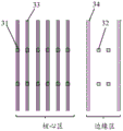
在一些实施例中,参照图8a和图8b所示,沿第一方向,图案化处理后的第二掩膜层中包括等间距排布的多个第三预设图案33和等间距排布的多个第四预设图案34;其中,相邻两个第四预设图案34之间的距离,等于相邻两个第三预设图案33之间的距离;In some embodiments, as shown in FIGS. 8 a and 8 b , along the first direction, the patterned second mask layer includes a plurality of third
沿第一方向,图案化处理后的第一掩膜层中包括等间距排布的多个第一预设图案31和等间距排布的多个第二预设图案32;其中,Along the first direction, the patterned first mask layer includes a plurality of first
相邻两个第二预设图案32之间的距离,等于相邻两个第一预设图案31之间的距离;The distance between two adjacent second
或者,or,
相邻两个第二预设图案32之间的距离,等于相邻两个第一预设图案31之间距离的2倍。The distance between two adjacent second
参照图8a所示,相邻两个第一预设图案31之间的间距等于相邻两个第三预设图案33之间的间距,相邻两个第二预设图案32之间的间距等于相邻两个第四预设图案34之间的间距,且第二预设图案32位于第四预设图案34之间的间隙的中点处,即第二预设图案32到与其相邻的两个第四预设图案34的距离相等。Referring to FIG. 8a, the spacing between two adjacent first
参照图8b所示,相邻两个第一预设图案31之间的间距等于相邻两个第三预设图案33之间的间距,且等于相邻两个第四预设图案34之间的间距。相邻两个第二预设图案32之间的间距为相邻两个第一预设图案31之间距离的2倍,且第二预设图案32位于第四预设图案34之间的间隙的中点处。Referring to FIG. 8 b , the spacing between two adjacent first
相关技术中,通常可在边缘区和核心区形成间距相同且尺寸相同的接触孔结构,并且,在边缘区和核心区对应形成覆盖接触孔的金属导线结构。In the related art, usually, contact hole structures with the same spacing and the same size can be formed in the edge region and the core region, and metal wire structures covering the contact holes are correspondingly formed in the edge region and the core region.
本公开实施例提供的方案,通过对边缘区中两组接触孔结构相对金属导线结构平移半节距(half pitch)距离,设计出用于形成第一预设图案的掩膜版。需要强调的是,此时,用于形成金属导线结构的掩膜版布局不变。In the solution provided by the embodiments of the present disclosure, a mask for forming the first preset pattern is designed by translating the two groups of contact hole structures in the edge region by a half pitch distance relative to the metal wire structure. It should be emphasized that, at this time, the mask layout for forming the metal wire structure remains unchanged.
在一些实施例中,两组接触孔可以沿平行于x轴的方向同向平移,且用于形成金属导线结构的掩膜版布局不变时,形成的第一预设图案和第二预设图案之间的关系如图8a所示。In some embodiments, the two groups of contact holes can be translated in the same direction along the direction parallel to the x-axis, and the first preset pattern and the second preset pattern are formed when the mask layout for forming the metal wire structure remains unchanged. The relationship between the patterns is shown in Fig. 8a.
在另一些实施例中,相邻的两组接触孔可以沿平行于x轴的方向反向平移,且用于形成金属导线结构的掩膜版布局不变时,形成的第一预设图案和第二预设图案之间的关系如图8b所示。In other embodiments, the adjacent two groups of contact holes can be reversely translated along the direction parallel to the x-axis, and when the layout of the mask used for forming the metal wire structure remains unchanged, the first preset pattern and The relationship between the second preset patterns is shown in FIG. 8b.
在一些实施例中,参照图9a和图9b所示,沿第一方向,图案化处理后的第一掩膜层中包括等间距排布的多个第一预设图案31,以及等间距排布的多个第二预设图案32;其中,相邻两个第二预设图案32之间的距离,等于相邻两个第一预设图案31之间的距离;In some embodiments, referring to FIGS. 9 a and 9 b , along the first direction, the patterned first mask layer includes a plurality of first
沿所述第一方向,图案化处理后的第二掩膜层中包括等间距排布的多个第三预设图案33和等间距排布的多个第四预设图案34;其中,相邻两个第四预设图案34之间的距离,等于相邻两个第三预设图案33之间距离的3倍。Along the first direction, the patterned second mask layer includes a plurality of third
示例性地,参照图9a所示,相邻两个第二预设图案32之间的间距与相邻两个第一预设图案31之间的间距相等,相邻两个第四预设图案34之间的间距为相邻两个第三预设图案33之间间距的3倍,第四预设图案34到与其相邻的第二预设图案32之间的间距等于相邻两个第二预设图案32之间的间距。Exemplarily, referring to FIG. 9a, the spacing between two adjacent second
在一些实施例中,第四预设图案34到与其相邻的第二预设图案32之间的间距也可以不相等。In some embodiments, the spacing between the fourth
示例性地,参照图9b所示,相邻两个第二预设图案32之间的间距与相邻两个第一预设图案31之间的间距相等,第四预设图案34位于第二预设图案32 之间的间隙的中点位置,即第四预设图案34到与其相邻的第二预设图案32之间的间距相等,且相邻两个第四预设图案34之间的间距,等于相邻两个第三预设图案33之间距离的3倍。Exemplarily, referring to FIG. 9b, the distance between two adjacent second
本公开实施例提供的方案,通过边缘区中两组金属导线结构的缺失,设计出用于形成第二预设图案的掩膜版。In the solution provided by the embodiments of the present disclosure, a mask for forming the second predetermined pattern is designed by the absence of two groups of metal wire structures in the edge region.
在一些实施例中,通过边缘区中两组金属导线结构的缺失,且用于形成接触孔结构的掩膜版布局不变时,形成的第一预设图案和第二预设图案之间的关系如图9a所示。In some embodiments, the gap between the first preset pattern and the second preset pattern is formed by the absence of two groups of metal wire structures in the edge region and the mask layout for forming the contact hole structure remains unchanged. The relationship is shown in Figure 9a.
在另一些实施例中,通过边缘区中两组金属导线结构的缺失,且两组接触孔可以沿平行于x轴的方向同向平移时,形成的第一预设图案和第二预设图案之间的关系如图9b所示。In other embodiments, the first preset pattern and the second preset pattern are formed by the absence of two groups of metal wire structures in the edge region and the two groups of contact holes can be translated in the same direction along the direction parallel to the x-axis. The relationship between them is shown in Fig. 9b.
在一些实施例中,第四预设图案34到与其相邻的第二预设图案32之间的间距也可以不相等,或者第四预设图案34到与其相邻的第二预设图案32之间的间距也可以不等于相邻的第二预设图案32之间的间距。In some embodiments, the spacing between the fourth
图10为根据一示例性实施例示出的一种半导体器件100的示意图,半导体器件100采用上述任一实施例所述的方法制备而成。图10为半导体器件100 在xoz平面内的局部截面示意图,参照图10所示,半导体器件100包括:FIG. 10 is a schematic diagram illustrating a
位于基底101的核心区的第一图案110;the
位于基底101的边缘区的第二图案120,第一图案110和第二图案120尺寸相同,且第一图案110与第二图案120沿第一方向并列排布且具有第一预设距离d1;其中,第一方向平行于基底101;The
位于核心区的第三图案130,第三图案130贯穿覆盖基底101的介质层102;且第三图案130与第一图案110沿第一方向一一对应重叠布置;the
位于边缘区的第四图案140,第四图案140贯穿介质层102;第三图案130 和第四图案140尺寸相同,且第三图案130和第四图案140沿第一方向并列排布且具有第二预设距离d2;第四图案140与第二图案120沿第一方向错开;The
其中,第二图案120与第四图案140,用于确定第一图案110与第三图案 130的对位偏差。The
示例性地,基底101的核心区包括形成有功能电路结构的功能区,核心区周围的边缘区包括位于核心区周围不形成功能电路的区域。可以理解的是,边缘区不发挥电学功能。Exemplarily, the core area of the
示例性地,第一图案110与第二图案120是位于同一层不同区域的相同图案,可通过同一掩膜版同时形成,第三图案130与第四图案140是位于同一层不同区域的相同图案,可通过同一掩膜版同时形成。Exemplarily, the
沿第一方向(平行于x方向)第二图案120与第四图案140不重叠,第二图案120和第四图案140不发挥电学功能,可用于确定第三图案130与第一图案110之间的对位偏差。Along the first direction (parallel to the x direction) the
示例性地,第三图案130和第四图案140可通过先形成覆盖基底101的图案材料层,再通过光刻和刻蚀工艺将图案材料层图形化得到第三图案130和第四图案140。由于沿第一方向,第二图案120和第四图案140是完全错开的,因此,可直接检测第二图案120和第四图案140的位置信息。Exemplarily, the
因此,可在制备半导体器件100的过程中,可量测第二图案120和第四图案140之间的偏移距离,即实际形成的第二图案120和第四图案140之间实际距离。第一预设距离d1与第二预设距离d2的差值可表示第二图案120和第四图案140之间的预设距离,通过第二图案120和第四图案140之间的实际距离与预设距离,可得到第二图案120和第四图案140之间的沿第一方向的位置偏差,进而得到第一图案110与第三图案130的对位偏差。Therefore, in the process of fabricating the
在一些实施例中,即使在第二图案120上形成较薄的介质层102后,光线可以穿透介质层102,也可以直接量测第二图案120的位置。In some embodiments, even after the
本公开实施例通过在核心区周围的边缘区设置与核心区第一图案尺寸相同的第二图案,并在核心区周围的边缘区设置与核心区第三图案尺寸相同的第四图案,且第一图案与第二图案之间具有第一预设距离,第三图案与第四图案之间具有第二预设距离,第二图案不与第四图案重叠,在制备半导体器件过程中,即使在无法直接量测第一图案与第三图案之间的对位偏差的情况下,可直接量测第二图案与第四图案在第一方向的偏移距离,并结合第一预设距离和第二预设距离,可以得到第一图案与第三图案的真实对位偏差。In the embodiment of the present disclosure, a second pattern with the same size as the first pattern in the core region is arranged in the edge region around the core region, and a fourth pattern with the same size as the third pattern in the core region is arranged in the edge region around the core region, and the third pattern is There is a first preset distance between a pattern and the second pattern, a second preset distance between the third pattern and the fourth pattern, and the second pattern does not overlap the fourth pattern. When the alignment deviation between the first pattern and the third pattern cannot be directly measured, the offset distance between the second pattern and the fourth pattern in the first direction can be directly measured, and the first preset distance and the third pattern can be combined. Two preset distances, the real alignment deviation between the first pattern and the third pattern can be obtained.
此外,本公开实施例中通过将第二图案和第四图案设置在核心区周围的边缘区,相较于在基底的核心区或者单独设置其它区域形成第二图案和第四图案,和相较于在基底的切割道区域或者其它区域单独形成特征尺寸较小、量测误差较大的对准标记,本公开利用核心区周围原本不形成功能电路的边缘区设置第二图案和第四图案,在不额外占用基底面积且不影响核心区面积的情况下,不仅实现了对于第一图案和第三图案对位偏差的量测,且减小了核心区的第一图案与第三图案的对位偏差的量测误差,提高了对位偏差量测的准确度和基底面积的利用率。In addition, in the embodiment of the present disclosure, by arranging the second pattern and the fourth pattern in the edge area around the core area, compared with forming the second pattern and the fourth pattern in the core area of the substrate or separately disposing other areas, and compared with In order to separately form alignment marks with smaller feature size and larger measurement error in the scribe line area or other areas of the substrate, the present disclosure utilizes the edge area around the core area where no functional circuit is originally formed to set the second pattern and the fourth pattern. Without additionally occupying the substrate area and without affecting the area of the core area, not only the measurement of the alignment deviation of the first pattern and the third pattern is realized, but also the alignment of the first pattern and the third pattern in the core area is reduced. The measurement error of the position deviation improves the accuracy of the position deviation measurement and the utilization rate of the substrate area.
在一些实施例中,沿第一方向,半导体器件100包括:In some embodiments, along the first direction, the
等间距排布的多个第三图案130和等间距排布的多个第四图案140;其中,沿第一方向,相邻两个第四图案140之间的距离,等于相邻两个第三图案130 之间的距离;A plurality of
等间距排布的多个第一图案110和等间距排布的多个第二图案120;其中,A plurality of
相邻两个第二图案120之间的距离,等于相邻两个第一图案110之间的距离;The distance between two adjacent
或者,or,
相邻两个第二图案120之间的距离,等于相邻两个第一图案110之间距离的2倍。The distance between two adjacent
示例性地,参照图11a所示,核心区中第一图案110与第三图案130一一对应重叠。等间距排布的多个第三图案130和等间距排布的多个第四图案140 位于基底101上介质层102中,相邻两个第四图案140之间的距离,等于相邻两个第三图案130之间的距离。第一图案110与第二图案120位于基底101中,相邻两个第二图案120之间的距离,等于相邻两个第一图案110之间的距离。Exemplarily, as shown in FIG. 11 a , the
图11a中虚线框为核心区中的一个预设子区域R1,边缘区中第二图案 120-1、120-2、120-3、120-4分别与预设子区域R1内的第一图案110-1、110-2、 110-3、110-4一一对应具有第一预设距离,边缘区中第四图案140-1、140-2、 140-3、140-4与预设子区域R1内的第三图案130-1、130-2、130-3、130-4一一对应具有第二预设距离,且第二图案120-1、120-2、120-3、120-4与第四图案 140-1、140-2、140-3、140-4沿第一方向(平行于x方向)相互错开不重叠。优选地,第四图案140-1与第二图案120-1之间的距离,等于第四图案140-1与第二图案120-2之间的距离。The dotted box in FIG. 11a is a preset sub-region R1 in the core region, the second patterns 120-1, 120-2, 120-3, 120-4 in the edge region are respectively the same as the first pattern in the preset sub-region R1 110-1, 110-2, 110-3, 110-4 have a one-to-one correspondence with a first preset distance, and the fourth patterns 140-1, 140-2, 140-3, 140-4 in the edge area and the preset The third patterns 130-1, 130-2, 130-3, 130-4 in the region R1 have a second predetermined distance in a one-to-one correspondence, and the second patterns 120-1, 120-2, 120-3, 120- 4 and the fourth patterns 140-1, 140-2, 140-3, 140-4 are staggered and not overlapped with each other along the first direction (parallel to the x direction). Preferably, the distance between the fourth pattern 140-1 and the second pattern 120-1 is equal to the distance between the fourth pattern 140-1 and the second pattern 120-2.
示例性地,参照图11b所示,等间距排布的多个第三图案130和等间距排布的多个第四图案140位于基底101上介质层102中,相邻两个第四图案140 之间的距离,等于相邻两个第三图案130之间的距离。第一图案110与第二图案120位于基底101中,相邻两个第二图案120之间的距离,等于相邻两个第一图案110之间距离的2倍。11b, a plurality of
图11b中虚线框为核心区中的一个预设子区域R2,边缘区中第二图案 120-1、120-2分别与预设子区域R1内的第一图案110-1、110-3一一对应具有第一预设距离,或者,边缘区中第二图案120-1、120-2分别与预设子区域R1 内的第一图案110-2、110-4一一对应具有第一预设距离,边缘区中第四图案 140-1、140-2、140-3、140-4分别与预设子区域R1内的第三图案130-1、130-2、 130-3、130-4一一对应具有第二预设距离,且第二图案120-1、120-2与第四图案140-1、140-2、140-3、140-4沿第一方向(平行于x方向)相互错开不重叠。优选地,第二图案120-1与第四图案140-1之间的距离,等于第二图案120-1 与第四图案140-2之间的距离。The dotted box in FIG. 11b is a preset sub-region R2 in the core region, and the second patterns 120-1 and 120-2 in the edge region are respectively the same as the first patterns 110-1 and 110-3 in the preset sub-region R1. There is a first predetermined distance in a one-to-one correspondence, or the second patterns 120-1 and 120-2 in the edge region have a first predetermined distance in a one-to-one correspondence with the first patterns 110-2 and 110-4 in the predetermined sub-region R1, respectively. Set the distance, the fourth patterns 140-1, 140-2, 140-3, 140-4 in the edge area are respectively connected to the third patterns 130-1, 130-2, 130-3, 130- in the preset sub-region R1 4 have a second preset distance in a one-to-one correspondence, and the second patterns 120-1, 120-2 and the fourth patterns 140-1, 140-2, 140-3, 140-4 are along the first direction (parallel to the x direction ) are staggered and do not overlap each other. Preferably, the distance between the second pattern 120-1 and the fourth pattern 140-1 is equal to the distance between the second pattern 120-1 and the fourth pattern 140-2.
在一些实施例中,沿第一方向,半导体器件100包括:In some embodiments, along the first direction, the
等间距排布的多个第一图案110和等间距排布的多个第二图案120;其中,相邻两个第二图案120之间的距离,等于相邻两个第一图案110之间的距离;A plurality of
等间距排布的多个第三图案130和等间距排布的多个第四图案140;其中,A plurality of
沿第一方向,相邻两个第四图案140之间的距离,等于相邻两个第三图案 130之间距离的3倍。Along the first direction, the distance between two adjacent
示例性地,参照图12a所示,核心区中第一图案110与第三图案130一一对应重叠,相邻两个第二图案120之间的距离等于相邻两个第一图案110之间的距离,相邻两个第四图案140之间的距离等于相邻两个第三图案130之间距离的3倍。边缘区中第二图案120-1、120-2分别与核心区预设子区域R3内的第一图案110-2、110-3一一对应具有第一预设距离,或者第二图案120-1、120-2 分别与预设子区域R3内的第一图案110-1、110-2一一对应具有第一预设距离,或者第二图案120-1、120-2分别与预设子区域R3内的第一图案110-3、110-4一一对应具有第一预设距离。边缘区中第四图案140-1、140-2分别与预设子区域R3内的第三图案130-1、130-4一一对应具有第二预设距离。优选地,第四图案140-1与第二图案120-1之间的距离等于第二图案120-1与第二图案120-2 之间的距离。Exemplarily, as shown in FIG. 12 a , the
示例性地,参照图12b所示,核心区中第一图案110与第三图案130一一对应重叠,相邻两个第二图案120之间的距离等于相邻两个第一图案110之间的距离,相邻两个第四图案140之间的距离等于相邻两个第三图案130之间距离的3倍。边缘区中第二图案120-1、120-2、120-3、120-4分别与核心区预设子区域R4内的第一图案110-1、110-2、110-3、110-4一一对应具有第一预设距离,边缘区中第四图案140-1、140-2分别与预设子区域R3内的第三图案130-1、 130-4一一对应具有第二预设距离。优选地,第四图案140-1与第二图案120-1 之间的距离,等于第四图案140-1与第二图案120-2之间的距离。Exemplarily, as shown in FIG. 12 b , the
以上所述,仅为本公开的具体实施方式,但本公开的保护范围并不局限于此,任何熟悉本技术领域的技术人员在本公开揭露的技术范围内,可轻易想到变化或替换,都应涵盖在本公开的保护范围之内。因此,本公开的保护范围应以所述权利要求的保护范围为准。The above are only specific embodiments of the present disclosure, but the protection scope of the present disclosure is not limited to this. should be included within the scope of protection of the present disclosure. Therefore, the protection scope of the present disclosure should be based on the protection scope of the claims.
Claims (11)
Priority Applications (1)
| Application Number | Priority Date | Filing Date | Title |
|---|---|---|---|
| CN202110975123.7A CN113741154A (en) | 2021-08-24 | 2021-08-24 | Method for measuring alignment deviation, semiconductor device and method for manufacturing the same |
Applications Claiming Priority (1)
| Application Number | Priority Date | Filing Date | Title |
|---|---|---|---|
| CN202110975123.7A CN113741154A (en) | 2021-08-24 | 2021-08-24 | Method for measuring alignment deviation, semiconductor device and method for manufacturing the same |
Publications (1)
| Publication Number | Publication Date |
|---|---|
| CN113741154A true CN113741154A (en) | 2021-12-03 |
Family
ID=78732517
Family Applications (1)
| Application Number | Title | Priority Date | Filing Date |
|---|---|---|---|
| CN202110975123.7A Pending CN113741154A (en) | 2021-08-24 | 2021-08-24 | Method for measuring alignment deviation, semiconductor device and method for manufacturing the same |
Country Status (1)
| Country | Link |
|---|---|
| CN (1) | CN113741154A (en) |
Cited By (5)
| Publication number | Priority date | Publication date | Assignee | Title |
|---|---|---|---|---|
| CN114695121A (en) * | 2022-02-24 | 2022-07-01 | 上海华力集成电路制造有限公司 | Method for measuring etching deviation of hard mask layer in self-aligned imaging process |
| WO2023206647A1 (en) * | 2022-04-27 | 2023-11-02 | 长鑫存储技术有限公司 | Semiconductor defect judgment method, computer device and readable storage medium |
| TWI835363B (en) * | 2022-10-24 | 2024-03-11 | 華邦電子股份有限公司 | Semiconductor wafer, processing apparatus for overlay shift and processing method thereof |
| CN119148470A (en) * | 2023-06-14 | 2024-12-17 | 中芯国际集成电路制造(上海)有限公司 | Overlay error measurement method, system, equipment and storage medium |
| CN120406058A (en) * | 2025-06-24 | 2025-08-01 | 长鑫新桥存储技术有限公司 | Measurement method of overlay error |
Citations (9)
| Publication number | Priority date | Publication date | Assignee | Title |
|---|---|---|---|---|
| CN101592869A (en) * | 2008-05-29 | 2009-12-02 | 中芯国际集成电路制造(北京)有限公司 | Exposure equipment focal distance monitoring method |
| CN102692830A (en) * | 2011-03-24 | 2012-09-26 | 南亚科技股份有限公司 | Method for evaluating alignment error and mask thereof |
| CN103035567A (en) * | 2011-10-07 | 2013-04-10 | 乐金显示有限公司 | Substrate for display device and method for manufacturing the same |
| CN105867066A (en) * | 2016-06-27 | 2016-08-17 | 京东方科技集团股份有限公司 | Mask plate, manufacturing method of display substrate, display substrate and display device |
| US20160334208A1 (en) * | 2015-05-12 | 2016-11-17 | United Microelectronics Corp. | Overlay mark pattern and method of measuring overlay |
| CN109767994A (en) * | 2018-12-12 | 2019-05-17 | 信利半导体有限公司 | Oled substrate and its pattern shift detection method, device |
| CN210778577U (en) * | 2019-09-27 | 2020-06-16 | 福建省晋华集成电路有限公司 | Semiconductor device and contact pad layout, contact pad structure and mask plate combination thereof |
| CN111522210A (en) * | 2020-06-03 | 2020-08-11 | 中科晶源微电子技术(北京)有限公司 | Overlay Alignment Mark, Overlay Error Measurement Method and Overlay Alignment Method |
| CN113093469A (en) * | 2020-01-08 | 2021-07-09 | 中芯国际集成电路制造(上海)有限公司 | Method for correcting target pattern, manufacturing mask and forming semiconductor structure |
-
2021
- 2021-08-24 CN CN202110975123.7A patent/CN113741154A/en active Pending
Patent Citations (9)
| Publication number | Priority date | Publication date | Assignee | Title |
|---|---|---|---|---|
| CN101592869A (en) * | 2008-05-29 | 2009-12-02 | 中芯国际集成电路制造(北京)有限公司 | Exposure equipment focal distance monitoring method |
| CN102692830A (en) * | 2011-03-24 | 2012-09-26 | 南亚科技股份有限公司 | Method for evaluating alignment error and mask thereof |
| CN103035567A (en) * | 2011-10-07 | 2013-04-10 | 乐金显示有限公司 | Substrate for display device and method for manufacturing the same |
| US20160334208A1 (en) * | 2015-05-12 | 2016-11-17 | United Microelectronics Corp. | Overlay mark pattern and method of measuring overlay |
| CN105867066A (en) * | 2016-06-27 | 2016-08-17 | 京东方科技集团股份有限公司 | Mask plate, manufacturing method of display substrate, display substrate and display device |
| CN109767994A (en) * | 2018-12-12 | 2019-05-17 | 信利半导体有限公司 | Oled substrate and its pattern shift detection method, device |
| CN210778577U (en) * | 2019-09-27 | 2020-06-16 | 福建省晋华集成电路有限公司 | Semiconductor device and contact pad layout, contact pad structure and mask plate combination thereof |
| CN113093469A (en) * | 2020-01-08 | 2021-07-09 | 中芯国际集成电路制造(上海)有限公司 | Method for correcting target pattern, manufacturing mask and forming semiconductor structure |
| CN111522210A (en) * | 2020-06-03 | 2020-08-11 | 中科晶源微电子技术(北京)有限公司 | Overlay Alignment Mark, Overlay Error Measurement Method and Overlay Alignment Method |
Cited By (6)
| Publication number | Priority date | Publication date | Assignee | Title |
|---|---|---|---|---|
| CN114695121A (en) * | 2022-02-24 | 2022-07-01 | 上海华力集成电路制造有限公司 | Method for measuring etching deviation of hard mask layer in self-aligned imaging process |
| WO2023206647A1 (en) * | 2022-04-27 | 2023-11-02 | 长鑫存储技术有限公司 | Semiconductor defect judgment method, computer device and readable storage medium |
| TWI835363B (en) * | 2022-10-24 | 2024-03-11 | 華邦電子股份有限公司 | Semiconductor wafer, processing apparatus for overlay shift and processing method thereof |
| CN119148470A (en) * | 2023-06-14 | 2024-12-17 | 中芯国际集成电路制造(上海)有限公司 | Overlay error measurement method, system, equipment and storage medium |
| CN119148470B (en) * | 2023-06-14 | 2025-10-24 | 中芯国际集成电路制造(上海)有限公司 | Overlay error measurement method, system, device and storage medium |
| CN120406058A (en) * | 2025-06-24 | 2025-08-01 | 长鑫新桥存储技术有限公司 | Measurement method of overlay error |
Similar Documents
| Publication | Publication Date | Title |
|---|---|---|
| CN113741154A (en) | Method for measuring alignment deviation, semiconductor device and method for manufacturing the same | |
| US7998826B2 (en) | Method of forming mark in IC-fabricating process | |
| KR100399597B1 (en) | Overlay Key and Method for Fabricating the Same and Method for measuring Overlay using the Same in process | |
| CN111522209B (en) | Overlay alignment mark and overlay error measurement method | |
| US6498401B2 (en) | Alignment mark set and method of measuring alignment accuracy | |
| CN113093479B (en) | Alignment measurement mark structure and alignment measurement method | |
| TW202013662A (en) | Asymmetric overlay mark for overlay measurement | |
| CN119620535B (en) | Semiconductor structure, forming method thereof and method for measuring overlay error | |
| KR19980079957A (en) | Shank pattern for inspection of buyer hole opening | |
| JP2000077312A (en) | Semiconductor device | |
| JP2007049074A (en) | Alignment error measurement mark and method for manufacturing semiconductor device using the same | |
| KR102617622B1 (en) | Overlay mark, overlay measurement method and semiconductor device manufacturing method using the overlay mark | |
| KR20120048904A (en) | Method measuring of overlay | |
| JPH04218918A (en) | Semiconductor device and its manufacture | |
| JPH11307418A (en) | Mask alignment mark and mask aligning method | |
| CN119002187B (en) | Overlay error measurement method, semiconductor process method and semiconductor structure | |
| JPH11283915A (en) | Method for manufacturing semiconductor device | |
| KR102750923B1 (en) | Overlay mark, overlay measurement method and semiconductor device manufacturing method using the overlay mark | |
| KR19990013281A (en) | A set of measurement patterns and methods for measuring dimensional accuracy and superposition accuracy of a circuit pattern | |
| JP2726411B2 (en) | Pattern drawing method | |
| JP2587614B2 (en) | Semiconductor device | |
| CN119148475A (en) | Method for improving overlay error performance in sheet and overlay mark | |
| JPH1167620A (en) | Semiconductor device having alignment mark | |
| CN121541413A (en) | Overlay markings, semiconductor structures and methods for preparing overlay markings | |
| KR100469910B1 (en) | A exposure mask and A method for forming a semiconductor device |
Legal Events
| Date | Code | Title | Description |
|---|---|---|---|
| PB01 | Publication | ||
| PB01 | Publication | ||
| SE01 | Entry into force of request for substantive examination | ||
| SE01 | Entry into force of request for substantive examination | ||
| RJ01 | Rejection of invention patent application after publication |
Application publication date: 20211203 |
|
| RJ01 | Rejection of invention patent application after publication |