Detailed Description
A planar transformer, magnetically coupled planar inductor, or coupled inductor circuit may employ u-shaped or horseshoe-shaped planar conductive traces to form a single turn of a transformer winding. The assembly of several layers of planar windings may allow for a very compact transformer circuit that may include output inductors such as for filtering.
Fig. 1 generally illustrates a schematic diagram of an example planar transformer system 100 according to the present subject matter. The planar transformer system 100 may include a planar transformer 101, a first set of switches (Q1-Q4), a second set of switches (M5-M8), output inductors 102, 103, 104, 105, and a controller 107. One or more of the first set of switches (Q1-Q4) or the second set of switches (M5-M8) may be accompanied by an optional gate driver 110. The planar transformer 101 may comprise a core 105, a first winding 106 and a second winding, such as may comprise two portions 111, 112. The first winding 106 may include a plurality of turns, and may typically include more than one turn. Each portion 111, 112 in the second winding may have a single turn.
The first winding may be a primary winding of a planar transformer or may be a secondary winding of a planar transformer. Unless otherwise specified, the first winding 106 is referred to as the primary winding. The first set of switches (Q1-Q4) may be controlled by the controller 107 and may be operable to repeatedly or periodically connect and disconnect the primary winding 106 from the voltage supply node and establish a circulating primary voltage across the first winding 106 and a circulating primary current through the first winding 106. The portions 111, 112 of the second winding may be magnetically coupled to the first winding 106 through the core 105. Core 105 may comprise an air core, a metal core, or other material capable of providing a flux linkage.
The controller 107 may control the first set of switches (Q1-Q4) and the second set of switches (M5-M8) to provide a voltage different from the input voltage (V8)IN) Output voltage (V)OUT). In the illustrated planar transformer system 100, the voltage (V) is outputOUT) Can be lower than the input voltage (V)IN) However, the subject matter is not limited thereto. When the planar transformer 101 operates as a step-down transformer, the controller 107 may control the first set of switches (Q1-Q4) to cause the input voltage (V) across the first winding 106IN) Oscillate or alternate in polarity. When the planar transformer 101 operates as a step-down transformer, the controller 107 may operate or synchronize the second set of switches (M5-M8) to extract power from the winding segments or portions of the second winding. The second set of switches (M5-M8) may be controlled with a two-phase signal (PH1, PH2), such as discussed below with reference to fig. 3. The output inductor may filter or smooth the periodic voltage and switching spikes generated on the second winding to provide a relatively constant output voltage. In some examples, output inductors 102, 103, 104, 105 may include, but are not limited to, magnetic core inductors, crystal core inductors, and the like.
Fig. 2 generally illustrates a signal waveform diagram illustrating an example of the operation of the planar transformer system 100 of fig. 1. The diagrams include the logic levels of the phase 1(PH1) and phase 2(PH2) signals controlling the switches (M5-M8) of the second winding, the voltage across the first winding (V2)1) Current in the first winding (I1), voltage at node (A, B, C, D) of the second winding (V)A、VB、VC、VD) And the output voltage (V) of the step-down transformerOUT)。
Typically, the transformer operates in one of the three phases to capture the output voltage induced by the first winding during transitions associated with the supply voltage applied to or isolated from the first winding. When the power supply voltage (V)IN) A change in current (I1) through the first winding, when applied to or isolated from the first winding, may induce a voltage across each second winding segment. The stepped down DC voltage can be captured at the output inductor by switching the connection of the second winding segment to capture the voltage induced when the current polarity of the first winding changes. The signal diagram assumes that a logic high level places each switch or transistor in a low impedance state (e.g., "on") and a logic low level places each switch in a high impedance state (e.g., "off"). However, switches or transistors that respond differently to logic commands may be used.
In FIG. 2, at t0The first winding circuit is in the first free rotation state, and the second winding circuit turns on all the switches (M5 to M8) "on" (e.g., PH1 — PH2 — high), and thus, each node (A, B, C, D) of the second winding is connected to ground. The "free spinning" state of the first winding allows any current in the first winding to continue to flow until terminated by a circuit loss. Any current in the output inductor (e.g., fig. 1, 102, 103) can be discharged to the output, or to the output voltage node (V)OUT) And (6) charging.
At t1The first winding circuit moves to a second state and the supply voltage may be at a first polarity (-V)IN) Applied across the first winding. Applying a supply voltage (V)IN) A change in current (I1) of the first winding may be induced and a voltage may be induced across the winding segments of the second winding. For example, a supply voltage (+ V) is applied to the first windingIN) A switch associated with a phase 2 control signal (PH2) (fig. 1; m6, M8) may be "disconnected". The change in current (I1) of the first winding may induce a voltage at the drains (B, D) of the switches (FIG. 3; M6, M8) associated with the phase 2 control signal (PH 2). The magnetic coupling of the planar first and second windings may beSo that the induced voltage (V) of each segment of the second windingB、VD) The supply voltage (V) applied to the first winding can be matchedIN) The sharp pulse shape of (2). At t1, the phase 2 signal (PH2) is low and the associated switch (M6, M8) is "off. The first winding 106 (or primary winding for the buck application) sees a voltage (e.g., V) across the winding terminalsIN) All of the variations of (a). The voltage across the connected winding segment of each of the second windings is given by:
where N is the turns ratio of the primary winding to each individual secondary winding. Assuming a load at the output terminals of the planar transformer system, the current in the output inductors 102, 103 may increase due to the positive voltage across them.
At t2The controller may switch the first winding back to the first free-wheeling state and the second winding circuit turn all switches (M5-M8) "on" (e.g., PH 1-PH 2-high "), thereby coupling each node of the second winding to ground. As previously described, any current flowing in the first winding continues to flow because the first winding inductance resists changes in the current flow. The current may drop slightly during the free-spinning state due to losses in the circuit. Any current in the output inductor (e.g., fig. 1, 102, 103) is discharged to the output terminal, or to the output voltage node (V)OUT) And (6) charging.
At t3The first winding circuit moves to a third state and the supply voltage (V)IN) May be of a second polarity (+ V)IN) Applied across the first winding. Applying a supply voltage (V)IN) A change in current (I1) of the first winding may be induced and a voltage may be induced across the segment of the second winding. For example, a supply voltage ((+ V) is applied across the first windingIN) The switch (M5, M7) associated with the phase 1 control signal (PH1) may be turned on or off in response to applying the supply voltage"open". The change in current (I1) of the first winding may induce a voltage at the drain (A, C) of the switch (FIG. 3; M5, M7) associated with the phase 1 control signal (PH 1). Magnetic coupling of the planar first and second windings may cause an induced voltage (V) at a node of the second windingC、VD) The supply voltage (V) applied to the first winding can be matchedIN) The sharp pulse shape of (2). At t3, the phase 1 signal (PH1) is low and the associated switch (M5, M7) is "off. The first winding 106 (or the primary winding for the buck application) experiences all changes in voltage across the winding terminals. The voltage across the connected winding segment of each of the second windings may be given by:
where N is the turns ratio of the primary winding to each individual secondary winding. Assuming a load at the output terminals of the planar transformer system, the current in the output inductors 102, 103 may increase due to the positive voltage across them.
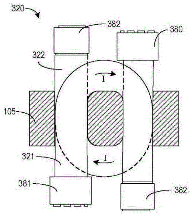
Fig. 3 generally illustrates an example layout 320 of conductive traces for a sub-portion of an example second winding in accordance with the present subject matter. For example, fig. 3 shows the overlap of two single-turn planar sub-portions 321, 322, which may form part of the second winding as discussed above (e.g., fig. 1, 111, 112). In some examples, the example layout 320 may include the core 105, the first sub-portion 321 of the first portion of the second winding, the first sub-portion 322 of the second portion of the second winding, the first and second inductors 382, 383, and the first and second switches 380, 381. Layout 320 may use nearly the same layout for each subsection 321, 322, but rotated 180 degrees from each other. The rotated, mirrored or complementary nature of the layout of each single- turn sub-portion 321, 322 allows inductors 382, 383 and switches 380, 381 to be compactly positioned with minimal, if any, additional routing of the conductive portions of each single- turn sub-portion 321, 322. This reduction in wiring allows each subsection to reduce or minimize losses compared to conventional layouts of planar transformers. Further, as current (I) is induced in each sub-portion 322, 321, the current (I) may flow in the same direction around the column of the core 105, thereby enhancing the magnetic coupling between the second winding and the first winding. While a single pair of subsections includes all of the nodes for coupling to the switch and inductor and may provide the basic boost or buck functionality, a second pair of subsections may allow for higher output currents with little, if any, increase in circuit footprint.
Fig. 4 illustrates a stacked configuration of an example planar transformer 400 according to the present subject matter. In this illustrative example, planar transformer 400 may include a 6:1 turns ratio between the first winding and the second winding, although the present subject matter is not limited in this respect. Planar transformer 400 may include a single core, although the present subject matter is not so limited. The stack may comprise 9 layers including five layers for routing six turns of the first winding and 4 layers for routing two pairs of sub-portions of the second winding (first winding a, first winding B).
Fig. 5A-5E generally illustrate the layout of the conductive portions of the first winding within each of the five layers of the example planar transformer 400 of fig. 4. Fig. 5A shows a first layout 551 of a portion of a first winding of an example planar transformer, the layout including a first conductive portion 531 routed to provide a single turn of the first winding. The first conductive portion 531 may have a first node 541 or a first set of vias for coupling to a voltage source or load and a second set of vias 542 for coupling to the second layer of the first winding. In some examples, the first node 541 may correspond to a first node of the intermediate nodes of the first set of switches (e.g., fig. 1, Q1-Q4). Fig. 5B generally illustrates a second layout 552 of a portion of the first winding of the example planar transformer of fig. 4. The second layer 552 may include the second conductive portion 532 of the first winding routed to provide a single turn or more of the first winding. A first end of the second conductive portion 532 may be electrically connected with the first conductive portion 531 of the first winding using the second set of vias 542. A second end of the second conductive portion 532 may be coupled to a third set of vias 543.
Fig. 5C generally illustrates a third layout 553 of a portion of the first winding of the example planar transformer 400 of fig. 4. The third layer 553 may comprise a third conductive portion 533 of the first winding that is routed to provide a single turn or more of the first winding. A first end of the third conductive portion 533 may be electrically connected with the second conductive portion 532 of the first winding using the third set of vias 543. A second end of the third conductive portion 533 may be coupled to a fourth set of vias 544.
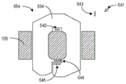
Fig. 5D generally illustrates a fourth layout 554 of a portion of the first winding of the example planar transformer 400 of fig. 4. Fourth layer 554 may include a fourth conductive portion 534 of the first winding routed to provide a single turn of the first winding. A first end of the fourth conductive portion 534 may be electrically connected to the third conductive portion 533 of the first winding using a fourth set of vias 544. A second end of the fourth conductive portion 534 may be coupled to a fifth set of vias 545.
Fig. 5E generally illustrates a fifth layout 555 of a portion of the first winding of the example planar transformer of fig. 4. The fifth layer 555 may include a fifth conductive portion 535 of the first winding routed to provide approximately one-half turn of the first winding. A first end of the fifth conductive portion 535 may be electrically connected to the fourth conductive portion 534 of the first winding using a fifth set of vias 545. A second end of the fifth conductive portion 535 may be coupled to a sixth set of vias 546. In certain examples, the sixth set of vias 546 may be at least a portion of the second node of the first winding and may correspond to the second node of the intermediate nodes of the first set of switches (e.g., fig. 1, Q1-Q4).
For the planar transformer 400 of fig. 4, nine layers are numbered incrementally from bottom to top, the first layout 551 of the first winding may be part of layer 4, the second layout 552 of the first winding may be part of layer 2, the third layout 553 of the first winding may be part of layer 7, the fourth layout 554 of the first winding may be part of layer 9, and the fifth layout 555 of the first winding may be part of layer 5. In the example shown, the series connection of each of the five layouts (551-555) of the first winding forms six turns around the center post of the core 105. It should be understood that other configurations of the portion including the same or different number of turns of the first winding are possible without departing from the scope of the present subject matter.
Fig. 6A and 6B generally illustrate layouts 660, 670 of sub-portions of the second winding of the example planar transformer 400 of fig. 4. Fig. 6A generally illustrates an example layout 660 of the first sub-portion 621 of the second winding. The layout 660 may include the core 105, the first conductive portion 661 routed to form a single turn of the second winding. The single turn planar conductor may substantially close the void with a smaller opening to the void to isolate the ends of the conductor. For example, the single turn planar conductor may be in the form of a "horseshoe" or other U-shape that is closed primarily around the central void but includes a gap to prevent complete closure around the central void. Some single turn planar conductors may have a "hook shape". Layout 660 may also include a first set of vias 671 and a second set of vias 672. The first set of vias 671 may be used to connect the first sub-portion 621 with a second parallel first sub-portion, one or more output inductors, one or more switches, or a combination thereof to form one of the two portions (111, 112) of the example planar transformer 400 of fig. 4. In some examples, layout 660 may be used for two of the nine layers of the example planar transformer 400 of fig. 4.
Fig. 6B generally illustrates an example layout 670 of the second sub-portion 622 of the second winding. The layout 670 may include the core 105, the second conductive portion 662 routed to form a single turn of the second winding. The single turn may be in the form of a "horseshoe" or "U". The orientation of the second conductive portion 662 may complement the orientation of the first conductive portion 661, or may generally mirror or reflect the orientation of the first conductive portion. Generally, the orientations of the first and second conductive portions 661, 662 are opposite to each other such that the direction of the end of one conductive portion is opposite to the direction of the corresponding end of the other conductive portion to allow a compact arrangement of the other parts of the second winding. As another example, the arrangement of the second conductive portion 662 may be referred to as rotated approximately 180 degrees when stacked and compared to a corresponding first sub-portion (e.g., layout 660) to support an overall, compact planar transformer. Layout 670 may also include a first set of vias 671 and a second set of vias 672. The second set of vias 672 may be used to connect the second sub-portion 622 with a second parallel second sub-portion, one or more inductors, one or more switches, or a combination thereof, to form one of the two portions (111, 112) of the example planar transformer 400 of fig. 4. The first set of vias 671 may be isolated from the second conductive portion 662 of the second winding and may be used to couple components of the second portion of the second winding together. In some examples, each portion of the second winding may include a greater or lesser number of planar conductive portions (e.g., 661, 662) to assist the second winding in being more closely coupled to the first winding.
With respect to the example planar transformer 400 of fig. 4, and numbering the nine layers incrementally from bottom to top, the example layout 660 of the first sub-portion of the second winding may be part of layers 1 and 8, and the example layout 670 of the second sub-portion of the second winding may be part of layers 3 and 6. In the example shown, a first part of the second winding may be formed by the parallel connection of layers 1 and 8, and a second part of the second winding may be formed by the parallel connection of layers 3 and 6. It should be understood that other configurations of the sub-portions of the second winding are possible without departing from the scope of the present subject matter. In some examples, each conductive portion 661, 662 may include additional conductive regions 663, 664 to assist in coupling the second winding with the first winding.
Fig. 7A and 7B generally illustrate various views of physical samples of an example planar transformer package according to the present subject matter. Fig. 7A shows a top view of an example planar transformer. The top view shows the multilayer substrate, the core, four inductors coupled to the second winding, the controller, and other control components, such as the drivers for the second set of switches. Fig. 7B illustrates a bottom view of an example planar transformer enclosure. The bottom view shows the multi-layer substrate, the core, the second set of switches, and additional secondary control components. In an example, the power density of a planar transformer according to the present subject matter may be greater than 50 kilowatts per liter (kW/L). This power density is provided by the complementary orientation of the respective sub-portions of the second winding, as discussed above. In an example, a planar transformer having a power density greater than 50 kilowatts/liter may provide a 3.3 volt output voltage of 140 amps from a 54 volt supply voltage. The overall size of such an example may be 24.5mm (l) x24mm (W) x15 mm.
Fig. 8 shows a conductive trace 880 of a layer having a portion of a second winding for an example planar transformer center tap configuration. In some examples, the conductive trace 880 may have a question mark type shape or a hook shape that approximates a single turn of the second winding. The shape allows control components such as the switch 881 and the inductor 882 associated with a portion of the second winding to be compactly arranged around the core 883.
Fig. 9 generally illustrates a circuit for an example planar transformer system 900 having a center tap configuration in accordance with the present subject matter. The planar transformer system 900 may include a planar transformer 901, a first set of switches (Q1-Q4), a second set of switches (M5-M8), output inductors 902, 903, and a controller 904. In some examples, one or more switches of the first and second sets of switches may be accompanied by a gate driver 910. Planar transformer 901 may include a core 905, a first winding 906, and one or more second windings 907, 908. The first winding 906 may include a plurality of turns, and may typically include more than one turn. Each second winding 907, 908 may include a plurality of winding segments 911, 912, 913, 914. Each winding segment 911, 912, 913, 914 may form a single turn of the second winding 907, 908. As used herein, a winding segment includes a primary conductive portion of a turn of the second winding and does not include auxiliary portions of the second winding, such as external terminals, fuses, switches, and the like.
The first winding may be a primary winding of a planar transformer or may be a secondary winding of a planar transformer. In fig. 9, the first winding 906 is referred to as a primary winding unless otherwise noted. A first set of switches (Q1-Q4) is controlled by the controller 904 and is operable to repeatedly or periodically connect and disconnect the primary winding 906 to and from the voltage supply rail and establish a circulating primary voltage across the first winding 906 and a circulating primary current through the first winding 906. The second windings 907, 908 may be magnetically coupled to the first winding 906 through a core 905. The core 905 may be an air core, a magnetic core with an air gap, or any material and structure capable of providing a flux linkage.
The controller 904 may control the first set of switches (Q1-Q4) and the second set of switches (M5-M8) to provide a voltage different from the input voltage (V) to provideIN) Output voltage (V)OUT). In the illustrated planar transformer system 900, the voltage (V) is outputOUT) Lower than the input voltage (V)IN) However, the subject matter is not limited thereto. When the planar transformer 901 operates as a step-down transformer, the controller 904 may control the first set of switches (Q1-Q4) to oscillate or alternate the polarity of the input Voltage (VIN) across the first winding 906. When the planar transformer 901 operates as a step-down transformer, the controller 904 may operate or synchronize the second set of switches (M5-M8) to extract power from the winding segments of the second winding. The second set of switches may be controlled using two-phase signals (PH1, PH 2). In certain examples, each second winding 907, 908 may be configured to include one or more taps (E, F) between connected winding segments (911/912 and 913/914). In some examples, taps (E, F) between winding segments may allow for an output voltage (V)OUT) Comprising an input voltage (V)IN) Step-up or step-down multipliers. Furthermore, the taps (E, F) between the connected winding segments (911/912 and 913/914) may help reduce the complexity or cost of the overall planar transformer design by using fewer switches as compared to conventional approaches and even more recent planar technologies. In addition, the taps (E, F) between the winding segments also allow the output voltage (V) to be smoothed using output inductors 902, 903 with much lower inductanceOUT). The lower inductance of the output inductors 902, 903 is provided by smoothing the output voltage (V) using the parasitic inductance of other planar transformer componentsOUT) Is generated by the circuit implementation of the output ripple. The output inductors 902, 903 may be coupled between corresponding taps (E, F) and output voltage terminals of the planar transformer system 900. In some examples, the output inductors 902, 903 may comprise air core inductors.
Fig. 10 generally illustrates an example compact layout 1090 for the second winding of the example circuit of fig. 9, including output inductors 902, 903 and a second set of switches (M5-M8). In some examples, the conductive traces or winding segments 911, 912, 913, 914 of each portion of the second winding may include respective conductive traces that may be located on multiple layers of the substrate of the example center-tapped planar transformer. The conductive traces associated with a particular winding segment of the second winding may be coupled together in parallel to handle higher currents because the additional layer of substrate provides a smaller increase in the vertical dimension of the transformer without increasing the planar footprint of the transformer.
Fig. 11 generally illustrates an example portion of a planar transformer 1100 configured to, for example, provide multiple voltage outputs. The example section generally shows a core 1105 comprising a plurality of posts, and sub-portions 1191, 1192, 1193, 1194 of the second winding surrounding each post. The portion of the planar transformer 1100 also shows a compact layout of the filter inductor (L) and the switch (S) for electrically coupling the sub-portions of the second winding as discussed above, for example to ensure that the current (I) on each sub-portion flows in the same direction as the corresponding leg around the core 1105. Using the techniques discussed above, the planar transformer 1100 can provide multiple output voltages or a single output voltage with greater output current capacity from a very small height multi-layer substrate package.
Fig. 12 generally illustrates a flow diagram of an example step-down method 1200 for operating a planar transformer according to the present subject matter. At 1201, a supply voltage may be applied with alternating polarity across a first planar winding of a planar transformer. The first planar winding may have a plurality of turns around the post of the metal core to induce a current in the second planar winding of the planar transformer. At 1203, a first node of the first single turn of the second winding may be coupled to ground via the first second winding switch in response to a first polarity of the supply voltage. The ground connection of the second winding may provide a reference potential for the induced voltage across the second winding. At 1205, the second node of the first single turn may be isolated from ground by a second switch in response to the first polarity of the supply voltage. Isolating the second node allows the current induced in the second winding to provide the output voltage of the planar transformer. At 1207, an output voltage may be provided at a first node of a first inductor coupled to the first single turn. The first inductor may be directly coupled in series with the first single turn at a second node of the first single turn. The first inductor for the buck configuration may provide filtering of the output voltage. In some examples, the current stored in the output inductor may assist in smoothing the output voltage level when the alternating polarity of the supply voltage is switched on the first planar winding.
In some examples, a single turn may include multiple parallel conductive traces. With a multilayer substrate, conductive traces can be stacked to provide a very space-saving planar transformer. Furthermore, by orienting some conductive traces 180 degrees relative to other conductive traces, the transformer power density may be increased without increasing the primary footprint of the planar transformer.
The foregoing detailed description includes reference to the accompanying drawings, which form a part hereof. The drawings show, by way of illustration, specific embodiments in which the invention may be practiced. These embodiments are also referred to herein as "examples". Such instances may include elements in addition to those shown or described. However, the inventors also contemplate examples in which only those elements shown or described are provided. Moreover, the inventors also contemplate examples using any combination or permutation of those elements shown or described (or one or more aspects thereof) with respect to a particular example (or one or more aspects thereof) or with respect to other examples (or one or more aspects thereof) shown or described herein.
In the event of a usage inconsistency between this document and any of the documents incorporated by reference, the usage in this document shall prevail.
In this document, the use of the terms "a" or "an" are used to include one or more than one, independent of any other instances or usages of "at least one" or "one or more," as is common in patent documents. In this document, unless otherwise indicated, the term "or" is used to mean a non-exclusive or, such that "a or B" includes: "A but not B", "B but not A", and "A and B". In this document, the terms "including" and "in which" are used as plain english equivalents of the respective terms "comprising" and "in wheein". Likewise, the terms "comprising" and "including" are open-ended, i.e., a system, device, article, composition, formulation, or process that includes elements in addition to those listed after such term is considered to be within the scope of the subject matter at issue. Furthermore, the terms "first," "second," and "third," etc., are used merely as labels, such as may appear in the claims, and are not intended to impose numerical requirements on their objects.
The method examples described herein may be machine or computer-implemented, at least in part. Some examples may include a computer-readable medium or machine-readable medium encoded with instructions operable to configure an electronic device to perform a method as described in the above examples. Implementations of such methods may include code, such as microcode, assembly language code, higher level language code, and the like. Such code may include computer readable instructions for performing various methods. The code may form part of a computer program product. Further, in an example, the code can be tangibly stored on one or more volatile, non-transitory, or non-volatile tangible computer-readable media, as during execution or at other times. Examples of such tangible computer-readable media may include, but are not limited to, hard disks, removable magnetic disks, removable optical disks (e.g., compact disks and digital video disks), magnetic tape, memory cards or sticks, Random Access Memories (RAMs), Read Only Memories (ROMs), and the like.
It is to be understood that the above description is intended to be illustrative, and not restrictive. For example, the above-described examples (or one or more aspects thereof) may be used in combination with each other. Other embodiments may be used, such as by one of ordinary skill in the art, upon reviewing the above description. The specification abstract is provided to comply with 37 c.f.r. § 1.72(b), to allow the reader to quickly ascertain the nature of the technical disclosure. It is submitted with the understanding that it will not be used to interpret or limit the scope or meaning of the claims. Also, in the above detailed description, various features may be combined together to simplify the present disclosure. This should not be interpreted as intending that an unclaimed disclosed function is essential to any claim. Rather, inventive subject matter may lie in less than all features of a particular disclosed embodiment. The following aspects are hereby incorporated into the detailed description as examples or embodiments, each independent as a separate embodiment, and it is contemplated that such embodiments may be combined with each other in various combinations or permutations.