CN113257755A - Package structure and method for forming the same - Google Patents
Package structure and method for forming the same Download PDFInfo
- Publication number
- CN113257755A CN113257755A CN202110322064.3A CN202110322064A CN113257755A CN 113257755 A CN113257755 A CN 113257755A CN 202110322064 A CN202110322064 A CN 202110322064A CN 113257755 A CN113257755 A CN 113257755A
- Authority
- CN
- China
- Prior art keywords
- chip
- layer
- package structure
- cavity
- heat dissipation
- Prior art date
- Legal status (The legal status is an assumption and is not a legal conclusion. Google has not performed a legal analysis and makes no representation as to the accuracy of the status listed.)
- Pending
Links
Images


Classifications
-
- H—ELECTRICITY
- H10—SEMICONDUCTOR DEVICES; ELECTRIC SOLID-STATE DEVICES NOT OTHERWISE PROVIDED FOR
- H10W—GENERIC PACKAGES, INTERCONNECTIONS, CONNECTORS OR OTHER CONSTRUCTIONAL DETAILS OF DEVICES COVERED BY CLASS H10
- H10W74/00—Encapsulations, e.g. protective coatings
- H10W74/10—Encapsulations, e.g. protective coatings characterised by their shape or disposition
- H10W74/111—Encapsulations, e.g. protective coatings characterised by their shape or disposition the semiconductor body being completely enclosed
- H10W74/114—Encapsulations, e.g. protective coatings characterised by their shape or disposition the semiconductor body being completely enclosed by a substrate and the encapsulations
-
- H—ELECTRICITY
- H10—SEMICONDUCTOR DEVICES; ELECTRIC SOLID-STATE DEVICES NOT OTHERWISE PROVIDED FOR
- H10W—GENERIC PACKAGES, INTERCONNECTIONS, CONNECTORS OR OTHER CONSTRUCTIONAL DETAILS OF DEVICES COVERED BY CLASS H10
- H10W40/00—Arrangements for thermal protection or thermal control
- H10W40/20—Arrangements for cooling
- H10W40/22—Arrangements for cooling characterised by their shape, e.g. having conical or cylindrical projections
- H10W40/226—Arrangements for cooling characterised by their shape, e.g. having conical or cylindrical projections characterised by projecting parts, e.g. fins to increase surface area
-
- H—ELECTRICITY
- H10—SEMICONDUCTOR DEVICES; ELECTRIC SOLID-STATE DEVICES NOT OTHERWISE PROVIDED FOR
- H10W—GENERIC PACKAGES, INTERCONNECTIONS, CONNECTORS OR OTHER CONSTRUCTIONAL DETAILS OF DEVICES COVERED BY CLASS H10
- H10W78/00—Detachable holders for supporting packaged chips in operation
Landscapes
- Cooling Or The Like Of Semiconductors Or Solid State Devices (AREA)
Abstract
The invention discloses a packaging structure and a forming method thereof. The package structure includes: a dielectric material having a cavity recessed from an upper surface of the dielectric material; a heat dissipation element located within the cavity; a chip located over the dielectric material and the heat dissipating element, and at least a portion of a bottom of the chip in contact with the heat dissipating element.
Description
Technical Field
The invention relates to the technical field of semiconductors, in particular to a packaging structure and a forming method thereof.
Background
In semiconductor technology, the application of embedded chips in system packaging has become more and more widespread. However, the heat dissipation requirements of the embedded chip are also increasing.
To increase the heat dissipation capability of the embedded chip, a large copper block is usually disposed in the substrate or a heat dissipation paste is introduced to expect heat to be conducted out of the package from the backside of the chip. As shown in fig. 1A, taking the embodiment of disposing the thermal paste 12 as an example, when performing die bonding, the die 14 may be at risk of cracking 18 due to unbalanced forces (as shown in fig. 1B), as shown in fig. 1B. Further, after the chip 14 is bonded, there is a possibility that a problem of chip inclination may occur.
Disclosure of Invention
In view of the above problems in the related art, the present invention provides a package structure and a method for forming the same, which can solve the problem of the inclination of the conventional chip when the chip is directly mounted on the heat dissipation element.
The technical scheme of the invention is realized as follows:
according to an aspect of the present invention, there is provided a package structure including: a dielectric material having a cavity recessed from an upper surface of the dielectric material; a heat dissipation element located within the cavity; a chip located over the dielectric material and the heat dissipating element, and at least a portion of a bottom of the chip in contact with the heat dissipating element.
In some embodiments, the chip spans over the cavity.
In some embodiments, a line structure is disposed in the dielectric material.
In some embodiments, the chip has a middle section in the length direction, and the heat dissipation element covers the bottom and the side of the middle section.
In some embodiments, the chip has two ends in the length direction, the sides of the two ends directly contacting the dielectric material and not contacting the heat dissipation element.
In some embodiments, the heat dissipation element protrudes beyond the chip in the width direction of the chip.
In some embodiments, the package structure further comprises: and the adhesive layer covers the dielectric material and the chip, wherein a space is arranged between the heat dissipation element and the dielectric material, and the adhesive layer is filled in the space.
In some embodiments, the sidewalls of the cavity are stepped.
In some embodiments, the heat-dissipating element completely fills the cavity to have a stepped sidewall.
In some embodiments, the heat dissipating element partially fills the cavity.
In some embodiments, the heat-dissipating element overfills the cavity.
In some embodiments, the chip has a middle section in the length direction, and the heat dissipation element has a maximum width at the middle section.
According to another aspect of the present invention, there is provided a package structure including: a dielectric layer having a cavity recessed from an upper surface of the dielectric layer; a heat dissipation element located within the cavity; a chip located over the dielectric layer and the heat dissipating element, and at least a portion of a bottom of the chip being in contact with the heat dissipating element; an electrical connector disposed on the chip; and the circuit layer is positioned above the chip, and the electric connector is used for electrically connecting the chip with the circuit layer.
In some embodiments, a line structure is disposed in the dielectric layer.
In some embodiments, the package structure further comprises: and a through hole passing through the dielectric layer and electrically connected to the circuit layer.
In some embodiments, the package structure further comprises: and the adhesive layer covers the dielectric layer and the chip, wherein a space is arranged between the heat dissipation element and the dielectric layer, and the adhesive layer is filled in the space.
According to another aspect of the present invention, there is provided a method of forming a package structure, including: forming a cavity recessed from an upper surface of the dielectric layer, and filling a heat dissipation material in the cavity; bonding a chip over the dielectric layer and the heat dissipating element, wherein at least a portion of the bottom of the chip is in contact with the heat dissipating element.
In some embodiments, between forming the cavity, further comprising: a line structure is formed in the dielectric layer.
In some embodiments, further comprising: forming a circuit layer; the chip is bonded to the wiring layer by electrical connections on the chip.
In some embodiments, after bonding the chip with the wiring layer, the method further comprises: forming a through hole through the line layer and to the line in the dielectric layer; the through hole is filled with a conductive material.
Drawings
In order to more clearly illustrate the embodiments of the present invention or the technical solutions in the prior art, the drawings needed in the embodiments will be briefly described below, and it is obvious that the drawings in the following description are only some embodiments of the present invention, and it is obvious for those skilled in the art to obtain other drawings without creative efforts.
Fig. 1A and 1B are schematic diagrams of a package structure formed according to the prior art.
Fig. 2 is a schematic diagram of a package structure implemented in accordance with the present invention.
Fig. 3A to 3D show schematic diagrams of various cross-sections of a package structure according to an embodiment of the invention.
Fig. 4A-4W are schematic diagrams of various stages in forming a package structure according to an embodiment of the invention.
Detailed Description
The technical solutions in the embodiments of the present invention will be clearly and completely described below with reference to the drawings in the embodiments of the present invention, and it is obvious that the described embodiments are only a part of the embodiments of the present invention, and not all of the embodiments. All other embodiments that can be derived by one of ordinary skill in the art from the embodiments given herein are intended to be within the scope of the present invention.
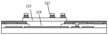
An embodiment in accordance with the present invention provides a package structure. Fig. 2 is a schematic diagram of a package structure implemented in accordance with the present invention. The package structure may include a dielectric material 112. The dielectric material 112 may be a single or multiple dielectric layers in the wiring layer 114, and in such embodiments, wiring structures are disposed in the dielectric material 112. In other embodiments, the dielectric material 112 may also be a dielectric material at other portions in the package structure. The dielectric material 112 has a cavity 116 recessed from an upper surface of the dielectric material 112. The sidewalls of the cavity 116 may be stepped. A heat dissipating element 118 is located within the cavity 116. The heat dissipating element 118 may completely fill the cavity 116, so that the heat dissipating element 118 accordingly has stepped side walls. In some embodiments, the ratio of the area of the bottom surface of the cavity 116 to the area of the heat dissipation element 118 in the top view is in the range of 70% to 90%. The thickness of the heat dissipation element 118 may be in the range of 5 microns to 20 microns. The length or width of the cavity 116 is in the range of 20 microns to 100 microns.
The chip 115 is positioned over the dielectric material 112 and the heat spreading element 118, and at least a portion of the bottom of the chip 115 is in contact with the heat spreading element 118. The chip 115 spans over the cavity 116. The heat dissipation member 118 may protrude from the chip 115 in a width direction of the chip 115. In some casesIn an embodiment, the material of the heat dissipation element 118 may include: metals, such as alloys of Ag, Cu, Au, Al, Ni, and combinations thereof; and/or non-metals, e.g. Ta2O5、SiO2、Al2O3。
In the above-mentioned technical solution of the present invention, a cavity 116 is formed in the dielectric material 112 and the heat dissipation element 118 is filled therein, and then the chip 115 is bonded to be in contact with the heat dissipation element 118, so that the level of the chip 115 is determined by the dielectric material 112, and the risk of tilting when the conventional chip 115 is directly mounted on the heat dissipation element 118 can be solved.
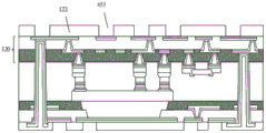
In the embodiment shown in fig. 2, the chip 115 is surrounded by the adhesive layer 111. The material of the adhesive layer 111 includes organic substances such as NCP, NCF, ACP, ACF, PI, epoxy, resin, pp, ABF, glue. The chip 115 is also connected to another wiring layer 120 over the adhesive layer 111 by a connection 113 (e.g., comprising solder) thereover. A solder mask layer 122 is disposed at exposed surfaces of the circuit layer 114 and the other circuit layer 120. The through-holes are connected to the wiring in the other wiring layer 120 through the wiring layer and the adhesive layer 111. The line layer 114 and the further line layer 120 may be RDL layers. The number of layers of the line layer 114 and the other line layer 120 may be any number, and the present invention is not limited thereto. It should be understood that the package structure may be any other applicable structure besides the configuration of the cavity 116, the heat dissipation element 118 and the chip 115.
Fig. 3A to 3D show schematic diagrams of various cross-sections of a package structure according to an embodiment of the invention. Fig. 3A is a top view of a cross section at line a-a in fig. 2. Fig. 3B, 3C and 3D are cross-sectional views at lines B-B, C-C and D-D in fig. 3A, respectively.
As shown in fig. 3A and 3B, the chip 115 has a middle section (corresponding to the line B-B in fig. 3A) and two end sections (corresponding to the line D-D in fig. 3A) in the length direction, and the heat dissipation member 118 covers the bottom of the middle section and also covers part of the side faces of the middle section. That is, at the middle section, the heat dissipation element 118 overfills the cavity 116 beyond the surface of the dielectric material 112. The heat dissipating member 118 has a maximum width at the position of the middle section of the chip 115, and gradually decreases in width in a direction extending from the middle section toward the end section. In fig. 3B, the top of the sidewalls of the cavity 116 may be in a range between 5 microns and 25 microns beyond the sidewalls of the chip 115.
As shown in fig. 3A and 3C, at a position between the middle section and the end section (corresponding to the line C-C in fig. 3A), the heat dissipation member 118 does not contact the side surface of the chip 115, but contacts the entire bottom surface of the chip 115. As shown in fig. 3A and 3D, at the ends of the chip 115, the sides of both ends directly contact the dielectric material 112 and do not contact the heat dissipation element 118. And where the heat spreading member 118 partially fills the cavity 116, there is a space between the heat spreading member 118 and the dielectric material 112 so that the adhesive layer 111 covering the chip 115 can be filled in the space.
Fig. 4A-4W are schematic diagrams of various stages in forming a package structure according to an embodiment of the invention. First, as shown in fig. 4A, a first carrier 401 is provided, a first seed layer 402 is disposed on the first carrier 401, and a first photoresist layer 403 is disposed on the first seed layer 402. In fig. 4B, the first photoresist layer 403 is patterned to form a first opening 404 in the first photoresist layer 403, and a first metal layer 405 is formed in the first opening 404. Then, the first photoresist layer 403 and the first seed layer 402 underlying the first photoresist layer 403 are removed, and a first dielectric layer 408 is formed on the remaining first seed layer 402 and the first metal layer 405, as shown in fig. 4C.
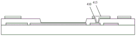
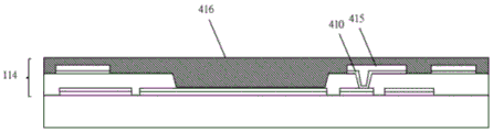
In fig. 4D, a second opening 409 is formed in the first dielectric layer 408, a second seed layer 410 is formed on the first dielectric layer 408 and within the second opening 409, and a second photoresist layer 412 is formed on the second seed layer 410. One of the second openings 409 corresponds to a subsequently formed cavity. In fig. 4E, a third opening 414 in the second photoresist layer 412 is formed, and a second metal layer 415 is formed in the third opening 414. Then, the second photoresist layer 412 and the second seed layer 410 positioned under the second photoresist layer 412 are removed, as shown in fig. 4F. In fig. 4G, a second dielectric layer 416 is formed on the remaining second seed layer 410 and second metal layer 415. Thereby forming the circuit layer 114.
In fig. 4H, a cavity 116 is formed in the first dielectric layer 408 and the second dielectric layer 416. The cavity 116 includes a second opening 409 in a first dielectric layer 408 formed as described above. In fig. 4I, a heat dissipation member 118 is filled in the cavity 116.
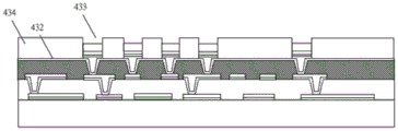
Next, as shown in fig. 4J, a patterned third seed layer 422 and a third metal layer 423, a third dielectric layer 425 covering the third seed layer 422 and the third metal layer 423 and having a third opening 424, a patterned fourth seed layer 426 and a fourth metal layer 428 may be formed on the second carrier 421 through similar steps as in fig. 4A to 4F. In fig. 4K, a fourth dielectric layer 429 is formed over the third dielectric layer, the fourth dielectric layer 429 having a fourth opening 431 exposing the underlying fourth metal layer 428. A fifth seed layer 432 is formed over the fourth dielectric layer 429 and within the fourth opening 428. In fig. 4L, a third photoresist layer 434 having a fifth opening 433 is formed on the fifth seed 432. A plurality of layers for forming a connection member are formed within the fifth opening 433. The third photoresist layer 434 and the fifth seed layer 432 under the third photoresist 434 are removed, thereby forming another line layer 120 and a connector 113 on the another line layer 120, as shown in fig. 4M. Device 435 is then engaged over connection 113.
The chip 115 is then attached to the heat-dissipating component 118 on the resulting structure of fig. 4I, as shown in fig. 4N. A plurality of connectors 113 are also disposed over the chip. In fig. 4O, the structure in fig. 4N is joined to the structure in fig. 4M by an adhesive layer 111. In fig. 4P, the first carrier 401 is removed. In fig. 4Q, a through hole 442 passing through the wiring layer 114, the adhesion layer 111, and reaching the wiring in the other wiring layer 120 is formed, and a sixth seed layer 443 is formed. In fig. 4R, a patterned fourth photoresist layer 445 exposing the through-hole 442 is formed over the line layer 114 and within the through-hole 442 to conformally form a fifth metal layer 446 within the through-hole. The fourth photoresist layer 445 and the sixth seed layer underlying the fourth photoresist layer 445 are removed, as shown in fig. 4S. In fig. 4T, solder mask layer 122 is formed, solder mask layer 122 having openings 452 exposing underlying circuitry. The resulting structure is then flipped and the second carrier 421 is removed, as in fig. 4U. In fig. 4V, another solder mask layer 122 is formed on the other wiring layer 120, the other solder mask layer 122 having an opening 453 exposing a wiring of the other wiring layer 120 therebelow. In fig. 4W, the seed layer exposed by the openings 452, 453 in the solder mask layers 122, 122 is removed by an etching process, forming a package structure.
The above description is only for the purpose of illustrating the preferred embodiments of the present invention and is not to be construed as limiting the invention, and any modifications, equivalents, improvements and the like that fall within the spirit and principle of the present invention are intended to be included therein.
Claims (10)
1. A package structure, comprising:
a dielectric material having a cavity recessed from an upper surface of the dielectric material;
a heat dissipating element located within the cavity;
a chip located over the dielectric material and the heat dissipating element, and at least a portion of a bottom of the chip in contact with the heat dissipating element.
2. The package structure of claim 1, wherein the chip has a middle section in a length direction, and the heat dissipation element covers a bottom and side surfaces of the middle section.
3. The package structure of claim 1, wherein the chip has two ends in a length direction, and sides of the two ends directly contact the dielectric material and do not contact the heat dissipation element.
4. The package structure of claim 1,
the heat dissipation member protrudes from the chip in a width direction of the chip.
5. The package structure of claim 1, further comprising:
an adhesive layer overlying the dielectric material and the chip,
wherein, the heat dissipation element and the dielectric material have a space therebetween, and the adhesive layer is filled in the space.
6. The package structure according to claim 1, wherein a sidewall of the cavity is stepped, and the heat dissipation member completely fills the cavity to have a stepped sidewall.
7. The package structure of claim 1, wherein the chip has a middle section in a length direction, and the heat dissipation element has a maximum width at the middle section.
8. A package structure, comprising:
a dielectric layer having a cavity recessed from an upper surface of the dielectric layer;
a heat dissipating element located within the cavity;
a chip located over the dielectric layer and the heat dissipating element, and at least a portion of a bottom of the chip being in contact with the heat dissipating element;
an electrical connector disposed on the chip;
and the circuit layer is positioned above the chip, the electric connector electrically connects the chip with the circuit layer, and a circuit structure is arranged in the dielectric layer.
9. A method of forming a package structure, comprising:
forming a cavity recessed from an upper surface of the dielectric layer, and filling a heat dissipation material in the cavity;
bonding a chip over the dielectric layer and the heat dissipating element, wherein at least a portion of a bottom of the chip is in contact with the heat dissipating element.
10. The method of forming a package structure of claim 9, further comprising:
forming a circuit layer;
bonding the chip to the wiring layer by electrical connections on the chip, further comprising, after bonding the chip to the wiring layer:
forming a through-hole through the line layer and to the line in the dielectric layer;
and filling a conductive material in the through hole.
Priority Applications (1)
| Application Number | Priority Date | Filing Date | Title |
|---|---|---|---|
| CN202110322064.3A CN113257755A (en) | 2021-03-25 | 2021-03-25 | Package structure and method for forming the same |
Applications Claiming Priority (1)
| Application Number | Priority Date | Filing Date | Title |
|---|---|---|---|
| CN202110322064.3A CN113257755A (en) | 2021-03-25 | 2021-03-25 | Package structure and method for forming the same |
Publications (1)
| Publication Number | Publication Date |
|---|---|
| CN113257755A true CN113257755A (en) | 2021-08-13 |
Family
ID=77181484
Family Applications (1)
| Application Number | Title | Priority Date | Filing Date |
|---|---|---|---|
| CN202110322064.3A Pending CN113257755A (en) | 2021-03-25 | 2021-03-25 | Package structure and method for forming the same |
Country Status (1)
| Country | Link |
|---|---|
| CN (1) | CN113257755A (en) |
Citations (9)
| Publication number | Priority date | Publication date | Assignee | Title |
|---|---|---|---|---|
| JP2011066116A (en) * | 2009-09-16 | 2011-03-31 | Panasonic Electric Works Co Ltd | Circuit module, and method of manufacturing the same |
| CN102148213A (en) * | 2011-03-08 | 2011-08-10 | 日月光半导体(威海)有限公司 | Lead frame of high-power chip package structure and manufacturing method thereof |
| US20120061808A1 (en) * | 2010-09-14 | 2012-03-15 | Guo-Cheng Liao | Semiconductor packages having increased input/output capacity and related methods |
| US20120086117A1 (en) * | 2010-10-06 | 2012-04-12 | Siliconware Precision Industries Co., Ltd. | Package with embedded chip and method of fabricating the same |
| US20120293977A1 (en) * | 2011-05-20 | 2012-11-22 | Subtron Technology Co. Ltd. | Package structure and manufacturing method thereof |
| CN104241372A (en) * | 2014-08-04 | 2014-12-24 | 台州市一能科技有限公司 | Wide bandgap semiconductor device and manufacturing method thereof |
| US20150262904A1 (en) * | 2014-03-14 | 2015-09-17 | Taiwan Semiconductor Manufacturing Company, Ltd. | Package with Embedded Heat Dissipation Features |
| US20170345714A1 (en) * | 2016-05-30 | 2017-11-30 | Infineon Technologies Ag | Chip carriers and semiconductor devices including redistribution structures with improved thermal and electrical performance |
| US20210074554A1 (en) * | 2019-09-09 | 2021-03-11 | Advanced Semiconductor Engineering, Inc. | Embedded component package structure and manufacturing method thereof |
-
2021
- 2021-03-25 CN CN202110322064.3A patent/CN113257755A/en active Pending
Patent Citations (9)
| Publication number | Priority date | Publication date | Assignee | Title |
|---|---|---|---|---|
| JP2011066116A (en) * | 2009-09-16 | 2011-03-31 | Panasonic Electric Works Co Ltd | Circuit module, and method of manufacturing the same |
| US20120061808A1 (en) * | 2010-09-14 | 2012-03-15 | Guo-Cheng Liao | Semiconductor packages having increased input/output capacity and related methods |
| US20120086117A1 (en) * | 2010-10-06 | 2012-04-12 | Siliconware Precision Industries Co., Ltd. | Package with embedded chip and method of fabricating the same |
| CN102148213A (en) * | 2011-03-08 | 2011-08-10 | 日月光半导体(威海)有限公司 | Lead frame of high-power chip package structure and manufacturing method thereof |
| US20120293977A1 (en) * | 2011-05-20 | 2012-11-22 | Subtron Technology Co. Ltd. | Package structure and manufacturing method thereof |
| US20150262904A1 (en) * | 2014-03-14 | 2015-09-17 | Taiwan Semiconductor Manufacturing Company, Ltd. | Package with Embedded Heat Dissipation Features |
| CN104241372A (en) * | 2014-08-04 | 2014-12-24 | 台州市一能科技有限公司 | Wide bandgap semiconductor device and manufacturing method thereof |
| US20170345714A1 (en) * | 2016-05-30 | 2017-11-30 | Infineon Technologies Ag | Chip carriers and semiconductor devices including redistribution structures with improved thermal and electrical performance |
| US20210074554A1 (en) * | 2019-09-09 | 2021-03-11 | Advanced Semiconductor Engineering, Inc. | Embedded component package structure and manufacturing method thereof |
Similar Documents
| Publication | Publication Date | Title |
|---|---|---|
| US10460958B2 (en) | Method of manufacturing embedded packaging with preformed vias | |
| US6611052B2 (en) | Wafer level stackable semiconductor package | |
| US5606198A (en) | Semiconductor chip with electrodes on side surface | |
| JP3258764B2 (en) | Method for manufacturing resin-encapsulated semiconductor device, external lead-out electrode and method for manufacturing the same | |
| US5668409A (en) | Integrated circuit with edge connections and method | |
| US20060278970A1 (en) | Semiconductor device, stacked semiconductor device, and manufacturing method for semiconductor device | |
| JP2017038075A (en) | Stackable molded ultra small electronic package including area array unit connector | |
| JP2009506572A (en) | Microfeature assemblies including interconnect structures and methods for forming such interconnect structures | |
| JP2006019433A (en) | Semiconductor device and manufacturing method thereof | |
| WO2005059998A1 (en) | Integrated circuits and packaging substrates with cavities, and attachment methods including insertion of protruding contact pads into cavities | |
| TWI858353B (en) | Signal-heat separation TMV packaging structure and its manufacturing method | |
| KR20050037430A (en) | Semiconductor package device and method of formation and testing | |
| CN118553709B (en) | Packaging substrate and manufacturing method thereof | |
| CN1319138C (en) | Method of forming a packaged semiconductor device | |
| JP4047819B2 (en) | Interconnection part using BGA solder ball and method for producing the same | |
| CN112838067B (en) | Chip packaging structure and manufacturing method thereof | |
| CN113257755A (en) | Package structure and method for forming the same | |
| US7122400B2 (en) | Method of fabricating an interconnection for chip sandwich arrangements | |
| CN101533818A (en) | Package structure of integrated circuit element and manufacturing method thereof | |
| CN1315168C (en) | Wafer Level Packaging Manufacturing Process and Its Wafer Structure | |
| CN111312665B (en) | Package structure and method for manufacturing the same | |
| KR100752665B1 (en) | Semiconductor device using conductive adhesive layer and its manufacturing method | |
| US20250183107A1 (en) | Semiconductor package | |
| TWI859642B (en) | Package structure, package substrate and manufacturing method thereof | |
| CN111863717B (en) | A chip interconnection method |
Legal Events
| Date | Code | Title | Description |
|---|---|---|---|
| PB01 | Publication | ||
| PB01 | Publication | ||
| SE01 | Entry into force of request for substantive examination | ||
| SE01 | Entry into force of request for substantive examination |