CN113075429A - Detection card, detection system and detection method - Google Patents
Detection card, detection system and detection method Download PDFInfo
- Publication number
- CN113075429A CN113075429A CN202010004449.0A CN202010004449A CN113075429A CN 113075429 A CN113075429 A CN 113075429A CN 202010004449 A CN202010004449 A CN 202010004449A CN 113075429 A CN113075429 A CN 113075429A
- Authority
- CN
- China
- Prior art keywords
- support member
- probe card
- optical fiber
- frame
- under test
- Prior art date
- Legal status (The legal status is an assumption and is not a legal conclusion. Google has not performed a legal analysis and makes no representation as to the accuracy of the status listed.)
- Pending
Links
- 238000001514 detection method Methods 0.000 title claims abstract description 32
- 239000000523 sample Substances 0.000 claims abstract description 161
- 239000013307 optical fiber Substances 0.000 claims abstract description 76
- 239000000835 fiber Substances 0.000 claims abstract description 10
- 238000012360 testing method Methods 0.000 claims description 98
- 238000000034 method Methods 0.000 claims description 19
- 230000003287 optical effect Effects 0.000 claims description 13
- 239000000919 ceramic Substances 0.000 claims description 4
- 239000011521 glass Substances 0.000 claims description 3
- 239000010408 film Substances 0.000 description 29
- 238000004519 manufacturing process Methods 0.000 description 4
- 229910052727 yttrium Inorganic materials 0.000 description 4
- 239000000203 mixture Substances 0.000 description 3
- 239000010409 thin film Substances 0.000 description 3
- XUIMIQQOPSSXEZ-UHFFFAOYSA-N Silicon Chemical compound [Si] XUIMIQQOPSSXEZ-UHFFFAOYSA-N 0.000 description 2
- 230000008054 signal transmission Effects 0.000 description 2
- 229910052710 silicon Inorganic materials 0.000 description 2
- 239000010703 silicon Substances 0.000 description 2
- 235000012431 wafers Nutrition 0.000 description 2
- RYGMFSIKBFXOCR-UHFFFAOYSA-N Copper Chemical compound [Cu] RYGMFSIKBFXOCR-UHFFFAOYSA-N 0.000 description 1
- 239000000956 alloy Substances 0.000 description 1
- 229910045601 alloy Inorganic materials 0.000 description 1
- 230000004075 alteration Effects 0.000 description 1
- 230000005540 biological transmission Effects 0.000 description 1
- 239000004020 conductor Substances 0.000 description 1
- 238000010276 construction Methods 0.000 description 1
- 229910052802 copper Inorganic materials 0.000 description 1
- 239000010949 copper Substances 0.000 description 1
- 230000002950 deficient Effects 0.000 description 1
- 238000010586 diagram Methods 0.000 description 1
- PCHJSUWPFVWCPO-UHFFFAOYSA-N gold Chemical compound [Au] PCHJSUWPFVWCPO-UHFFFAOYSA-N 0.000 description 1
- 229910052737 gold Inorganic materials 0.000 description 1
- 239000010931 gold Substances 0.000 description 1
- 239000011810 insulating material Substances 0.000 description 1
- 239000000463 material Substances 0.000 description 1
- 239000012528 membrane Substances 0.000 description 1
- 239000002184 metal Substances 0.000 description 1
- 229910052751 metal Inorganic materials 0.000 description 1
- 239000007769 metal material Substances 0.000 description 1
- 239000012811 non-conductive material Substances 0.000 description 1
- 239000004033 plastic Substances 0.000 description 1
- 239000004065 semiconductor Substances 0.000 description 1
- 238000006467 substitution reaction Methods 0.000 description 1
Images


Classifications
-
- G—PHYSICS
- G01—MEASURING; TESTING
- G01R—MEASURING ELECTRIC VARIABLES; MEASURING MAGNETIC VARIABLES
- G01R1/00—Details of instruments or arrangements of the types included in groups G01R5/00 - G01R13/00 and G01R31/00
- G01R1/02—General constructional details
- G01R1/06—Measuring leads; Measuring probes
- G01R1/067—Measuring probes
- G01R1/07—Non contact-making probes
- G01R1/071—Non contact-making probes containing electro-optic elements
-
- G—PHYSICS
- G01—MEASURING; TESTING
- G01R—MEASURING ELECTRIC VARIABLES; MEASURING MAGNETIC VARIABLES
- G01R31/00—Arrangements for testing electric properties; Arrangements for locating electric faults; Arrangements for electrical testing characterised by what is being tested not provided for elsewhere
- G01R31/28—Testing of electronic circuits, e.g. by signal tracer
- G01R31/2851—Testing of integrated circuits [IC]
- G01R31/2855—Environmental, reliability or burn-in testing
- G01R31/286—External aspects, e.g. related to chambers, contacting devices or handlers
- G01R31/2863—Contacting devices, e.g. sockets, burn-in boards or mounting fixtures
-
- G—PHYSICS
- G01—MEASURING; TESTING
- G01R—MEASURING ELECTRIC VARIABLES; MEASURING MAGNETIC VARIABLES
- G01R1/00—Details of instruments or arrangements of the types included in groups G01R5/00 - G01R13/00 and G01R31/00
- G01R1/02—General constructional details
- G01R1/06—Measuring leads; Measuring probes
- G01R1/067—Measuring probes
- G01R1/073—Multiple probes
-
- G—PHYSICS
- G01—MEASURING; TESTING
- G01R—MEASURING ELECTRIC VARIABLES; MEASURING MAGNETIC VARIABLES
- G01R1/00—Details of instruments or arrangements of the types included in groups G01R5/00 - G01R13/00 and G01R31/00
- G01R1/02—General constructional details
-
- G—PHYSICS
- G01—MEASURING; TESTING
- G01R—MEASURING ELECTRIC VARIABLES; MEASURING MAGNETIC VARIABLES
- G01R1/00—Details of instruments or arrangements of the types included in groups G01R5/00 - G01R13/00 and G01R31/00
- G01R1/02—General constructional details
- G01R1/06—Measuring leads; Measuring probes
- G01R1/067—Measuring probes
- G01R1/073—Multiple probes
- G01R1/07307—Multiple probes with individual probe elements, e.g. needles, cantilever beams or bump contacts, fixed in relation to each other, e.g. bed of nails fixture or probe card
- G01R1/07342—Multiple probes with individual probe elements, e.g. needles, cantilever beams or bump contacts, fixed in relation to each other, e.g. bed of nails fixture or probe card the body of the probe being at an angle other than perpendicular to test object, e.g. probe card
-
- G—PHYSICS
- G01—MEASURING; TESTING
- G01R—MEASURING ELECTRIC VARIABLES; MEASURING MAGNETIC VARIABLES
- G01R31/00—Arrangements for testing electric properties; Arrangements for locating electric faults; Arrangements for electrical testing characterised by what is being tested not provided for elsewhere
- G01R31/28—Testing of electronic circuits, e.g. by signal tracer
- G01R31/2851—Testing of integrated circuits [IC]
- G01R31/2886—Features relating to contacting the IC under test, e.g. probe heads; chucks
- G01R31/2889—Interfaces, e.g. between probe and tester
Landscapes
- Physics & Mathematics (AREA)
- General Physics & Mathematics (AREA)
- Engineering & Computer Science (AREA)
- Computer Hardware Design (AREA)
- Microelectronics & Electronic Packaging (AREA)
- General Engineering & Computer Science (AREA)
- Environmental & Geological Engineering (AREA)
- Testing Or Measuring Of Semiconductors Or The Like (AREA)
- Measuring Leads Or Probes (AREA)
Abstract
本发明公开一种探测卡、探测系统及探测方法。探测卡包括一框架;布置于该框架上并从此突出的一支撑构件;延伸通过该框架并进入该支撑构件的一开口;沿着该支撑构件布置并从此突出的一光纤和从该框架突出并布置在该光纤旁的许多探针。

The invention discloses a detection card, a detection system and a detection method. The probe card includes a frame; a support member disposed on the frame and protruding therefrom; an opening extending through the frame and into the support member; an optical fiber disposed along the support member and protruding therefrom and an optical fiber protruding from the frame and protruding from the frame A number of probes placed next to the fiber.
Description
Technical Field
The present invention relates generally to probe cards integrated with at least one optical fiber, and more particularly to thin film probe cards integrated with a Fiber Array Block (FAB). Further, the present invention relates to a probe system comprising a probe card integrated with at least one optical fiber, the probe card being disposed above the fixture and secured to a circuit board. Further, the present invention relates to a probing method for testing a Device Under Test (DUT) using a probe card integrated with at least one optical fiber.
Background
Semiconductor Devices Under Test (DUTs), such as wafers including dice, are tested by a probing system after fabrication. The probe card is used to test the electrical characteristics of the device under test to select and disregard any defective device under test. The probe card typically includes a plurality of probes protruding therefrom, wherein each probe is positioned in alignment with the corresponding contact pad above the device under test to accurately and consistently perform electrical testing.
However, the micro-scale of current devices under test makes testing of small and thin devices under test increasingly complex, including many steps and operations that are difficult to perform on such a scale. In addition, to reduce cost, probe cards are often equipped with more and more probes to contact multiple contact pads of a device under test, so that multiple dies can be tested simultaneously. Increased test complexity may reduce test accuracy.
Thus, there is a continuing need for improved probe card configurations and methods of probing.
The background discussion of the invention section merely provides background information. The statements in this background of the invention discussion are not admitted to constitute prior art to the present disclosure by the subject matter disclosed in this background of the invention discussion, and nothing in this background of the invention discussion is admitted to constitute prior art to the present disclosure by any section of this specification, including any discussion of the background of the invention section.
Disclosure of Invention
One embodiment of the present invention provides a probe card. The probe card includes a frame; a support member disposed on the frame and protruding therefrom; an opening extending through the frame and into the support member; an optical fiber disposed along and protruding from the support member and a plurality of probes protruding from the frame and disposed beside the optical fiber.
In some embodiments, the optical fiber is surrounded by the plurality of probes.
In some embodiments, the plurality of probes protrude from a dielectric film disposed on the frame and along the support member, and the optical fiber is surrounded by the dielectric film.
In some embodiments, the optical fiber is disposed within the opening or along a surface of the support member.
In some embodiments, the optical fiber is at least partially attached to the support member.
In some embodiments, the optical fiber is a Fiber Array Block (FAB) or includes a plurality of optical fibers.
In some embodiments, the support member is made of glass or ceramic.
In some embodiments, the dielectric film is at least partially attached to the support member.
In some embodiments, the support member is spaced apart from the plurality of probes.
In some embodiments, the dielectric film is flexible.
In some embodiments, the plurality of probes are electrically connected to a circuit board via a plurality of signal traces.
Another embodiment of the present invention provides a detection system. The detection system comprises a circuit board; a probe card including a frame fixedly attached to the circuit board, a support member protruding from the frame, an opening extending through the frame and the support member, an optical fiber disposed along the support member and protruding therefrom, and a plurality of probes protruding from the frame and disposed beside the optical fiber; and a fixture configured to support a Device Under Test (DUT), wherein the support member and the optical fiber are disposed above the fixture.
In some embodiments, the support member and the optical fiber are both surrounded by and protrude from the circuit board.
In some embodiments, one end of the optical fiber is aligned with a corresponding coupler on the device under test.
In some embodiments, the detection system further comprises a step disposed within the opening and configured to displace and orient the support member and the optical fiber.
In some embodiments, the support member is displaceable relative to the circuit board.
Another embodiment of the present invention provides a method of probing. The method includes providing a circuit board, a probe card above the circuit board, a fixture below the circuit board and the probe card, and a Device Under Test (DUT) on the fixture, wherein the probe card includes a frame secured to the circuit board, a support member protruding from the frame, an opening extending through the frame and the support member, an optical fiber disposed along and protruding from the support member, and a plurality of probes protruding from the frame and disposed beside the optical fiber; aligning an end portion of the optical fiber with a coupler above the device under test; and probing a plurality of pads over the DUT with the plurality of probes.
In some embodiments, the aligning comprises moving or rotating the support member relative to the device under test.
In some embodiments, the plurality of probes are used to probe the device under test by moving the support member towards the device under test, or moving the fixture and the device under test towards the probe card.
In some embodiments, the method further comprises: transmitting an optical signal to the device under test through the optical fiber; and transmitting a response signal from the device under test to the plurality of probes in response to the optical signal.
The foregoing has outlined rather broadly the features and technical advantages of the present invention in order that the detailed description of the invention that follows may be better understood. Additional features and advantages of the invention will be set forth in the description which follows, and in part will be apparent from the description, or may be learned by practice of the invention. It should be appreciated by those skilled in the art that the conception and specific embodiment disclosed may be readily utilized as a basis for modifying or designing other structures or processes for carrying out the same purposes of the present invention. It should also be realized by those skilled in the art that such equivalent constructions do not depart from the spirit and scope of the invention as set forth in the appended claims.
Drawings
The present invention will become more fully understood from the detailed description and the appended claims, taken in conjunction with the accompanying drawings, wherein like reference numerals refer to like elements throughout.
FIG. 1 is a schematic cross-sectional view of a thin film probe card in accordance with some embodiments of the present invention.
Fig. 2 is a schematic cross-sectional view of a cantilevered probe card in accordance with some embodiments of the present invention.
Fig. 3 is a schematic cross-sectional view of a vertical probe card in accordance with some embodiments of the present invention.
Fig. 4 is a schematic cross-sectional view of a detection system in accordance with some embodiments of the present invention.
Fig. 5 is a flow chart illustrating a detection method according to some embodiments of the invention.
Fig. 6-8 are schematic diagrams of the detection method of fig. 5, according to some embodiments of the invention.
Description of reference numerals:
100 first probe card
101 frame
101a first opening
102 support member
102a second opening
103 dielectric film
103a horizontal part
103b inclined part
103c end portion
104 buffer layer
105 signal line
106 probe
107 optical fiber
107a end portion
108 steps
109 fixer
110 fastening device
200 second probe card
201 circuit board
202 clamp
203 device under test
203a front side
203b back side
300 third probe card
400 detection system
Detailed Description
The following description of the disclosure is accompanied by the accompanying drawings, which are incorporated in and constitute a part of this specification, and which illustrate specific embodiments of the invention, but to which the invention is not limited. In addition, the following embodiments may be appropriately integrated to complete another embodiment.
References to "one embodiment," "an exemplary embodiment," "other embodiments," "another embodiment," etc., indicate that the embodiment includes a particular function, structure, or characteristic, but every embodiment may not necessarily include the particular function, structure, or characteristic. Further, repeated use of the phrase "in this embodiment" does not necessarily refer to the same embodiment, but may.
In the following description, specific steps and structures are provided in order to provide a thorough understanding of the present invention. It is apparent that embodiments of the invention are not limited to the specific details known to the skilled person. In other instances, well-known structures and steps have not been shown in detail in order not to unnecessarily obscure the present invention. The preferred embodiments of the present invention will be described in detail below. However, the invention may be practiced otherwise than as specifically described and illustrated in other specific embodiments. The scope of the invention is not to be limited by the details of the description but only by the claims.
In the present invention, a probe card is disclosed. The probe card includes an optical fiber supported by a support member, and a plurality of probes surrounding the optical fiber. The probe card is integrated with the optical fiber and the probes such that the probe card is suitable for silicon photonic probing. Allows the transmission of electrical and optical signals through the probe card and may increase or improve signal transmission speed. As a result, the test efficiency of the device under test can be improved.
In addition, the probe card may be integrated with a plurality of optical fibers or a Fiber Array Block (FAB) comprising a bundle of optical fibers. The probe card must be aligned with the device under test before probing or testing the device under test. In other words, each optical fiber is aligned with a corresponding component (e.g., coupler, pad, etc.) above the dut. In this manner, the alignment of the probe card results in the simultaneous alignment of all of the optical fibers. Therefore, time and effort spent on alignment can be reduced.
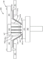
Fig. 1 is a schematic cross-sectional view of a first probe card 100 in accordance with various embodiments of the present invention. In some embodiments, the first probe card 100 is configured to perform testing of wafers, Devices Under Test (DUTs), dies, Integrated Circuits (ICs), and the like. In some embodiments, the first probe card 100 is configured to perform electrical, optical, or Radio Frequency (RF) testing. In some embodiments, the first probe card 100 is configured to be secured to a Printed Circuit Board (PCB), a flat panel, or the like. The first probe card 100 is integrated with at least one optical fiber 107. In this manner, the first probe card 100 allows high-speed signal transmission and efficient silicon photon detection. In some embodiments, the first probe card 100 is a thin film probe card.
In some embodiments, the first probe card 100 includes a frame 101. In some embodiments, the frame 101 has a rectangular, quadrilateral, or polygonal shape. In some embodiments, frame 101 is made of metal, alloy, ceramic, conductive material, non-conductive material, and the like. In some embodiments, the frame 101 is a rigid structure.
In some embodiments, the frame 101 includes a first opening 101a located on a central portion of the frame 101. In some embodiments, the first opening 101a extends through the frame 101. In some embodiments, the first opening 101a has a rectangular, quadrangular or polygonal shape.
In some embodiments, the first probe card 100 includes a support member 102 disposed on a frame 101. In some embodiments, the support member 102 protrudes from the frame 101. In some embodiments, the support member 102 is attached to an end of the first opening 101a of the frame 101. In some embodiments, the support member 102 tapers from the frame 101. In some embodiments, the support member 102 is made of glass, ceramic, plastic, or the like.
In some embodiments, the support member 102 includes a second opening 102a extending from the frame 101. In some embodiments, the second opening 102a is aligned with the first opening 101a of the frame 101 such that an opening extends through the frame 101 and into the support member 102.
In some embodiments, a dielectric film 103 is disposed on the frame 101 and the support member 102. In some embodiments, the dielectric film 103 is attached to the frame 101 and disposed along the support member 102. In some embodiments, the dielectric film 103 is spaced apart from the support member 102. In some embodiments, the dielectric film 103 is flexible and bendable. In some embodiments, the dielectric film 103 comprises a dielectric, polymeric, or insulating material. In some embodiments, the dielectric film 103 is transparent or translucent.
In some embodiments, the dielectric film 103 is at least partially attached to the frame 101 and the support member 102. In some particular embodiments, the horizontal portion 103a of the dielectric film 103 is disposed and attached to the frame 101, the inclined portion 103b of the dielectric film 103 is disposed along the outer surface of the support member 102, and the end portion 103c of the dielectric film 103 is attached to the support member 102. In some embodiments, the horizontal portion 103a is attached to the frame 101 by a buffer layer 104. In some embodiments, the buffer layer 104 includes a soft or deformable material.
In some embodiments, a number of signal lines 105 are disposed within the dielectric film 103. In some embodiments, the signal line 105 extends along the dielectric film 103. In some embodiments, the signal line 105 is configured to connect with a contact pad or circuit external to the first probe card 100. In some embodiments, signal line 105 is electrically conductive. In some embodiments, the signal lines 105 comprise a metallic material, such as copper, gold, or the like.
In some embodiments, a number of probes 106 protrude from the dielectric film 103. In some embodiments, the probe 106 pads are coupled to the signal lines 105, such that the probe 106 is electrically connected to a contact pad or circuit outside the first probe card 100 through the signal lines 105. In some embodiments, a signal (e.g., an electrical, RF, or optical signal) may be transmitted from an external circuit or manipulator to probe 106 via signal line 105. In some embodiments, the probe 106 is configured to transmit or receive a signal.
In some embodiments, the optical fiber 107 is disposed along the support member 102. In some embodiments, the optical fiber 107 is configured to transmit or receive an optical signal. In some embodiments, the optical fiber 107 is disposed on a surface of the support member 102. In some embodiments, the optical fibers 107 are elongated from the frame 101 and along the support member 102. In some embodiments, the optical fiber 107 is at least partially attached to the support member 102. In some embodiments, the optical fiber 107 is at least partially spaced from the support member 102. In some embodiments, the optical fiber 107 is surrounded by the probe 106. In some embodiments, the optical fiber 107 is surrounded by a dielectric film 103. In some embodiments, the optical fiber 107 is disposed within the second opening 102a of the support member 102.
In some embodiments, an end portion 107a of the optical fiber 107 protrudes from the support member 102. In some embodiments, end portion 107a of optical fiber 107 is configured to couple to a component (e.g., a coupler, etc.) above the device under test. In some embodiments, a Fiber Array Block (FAB) comprising a plurality of optical fibers 107 is disposed on the support member 102.
In some embodiments, a step 108 is disposed within the openings (101a and 102a) and is configured to displace and orient the support member 102 and the optical fiber 107. In some embodiments, support member 102 is movable along two axes (the X and Y axes) thereof. In some embodiments, support member 102 is movable along its three axes (X, Y and the Z axis). In some embodiments, support member 102 is rotatable about one or more of its three axes (X, Y and the Z axis). In some embodiments, the movement or rotation of the support member 102 may be operated manually or electrically (e.g., by one or more motors).
Fig. 2 is a schematic cross-sectional view of a second probe card 200 in accordance with various embodiments of the present invention. In some embodiments, the second probe card 200 is similar to the first probe card 100 except that the probes 106 of the second probe card 200 are held by a holder 109 and a fastening device 110. In some embodiments, the second probe card 200 is a cantilever probe card. In some embodiments, the probe 106 is disposed alongside the optical fiber 107. In some embodiments, the probe 106 surrounds the optical fiber 107 and the support member 102. In some embodiments, the second probe card 200 is a MEMS probe card and the probes 106 are MEMS probes.
Fig. 3 is a schematic cross-sectional view of a third probe card 300 in accordance with various embodiments of the present invention. In some embodiments, the third probe card 300 is similar to the first probe card 100 and the second probe card 200 except that the probes 106 of the third probe card 300 are vertical probes that protrude vertically from the third probe card 300. In some embodiments, the third probe card 300 is a vertical probe card.
FIG. 4 is a schematic cross-sectional view of a detection system 400 in accordance with many embodiments of the present invention. In some embodiments, the probe system 400 includes the first probe card 100, a circuit board 201, and a fixture 202. Fig. 4 illustrates the use of the first probe card 100 in the probe system 400, however, the invention is not limited to this embodiment. Those skilled in the art will readily appreciate that the second probe card 200, the third probe card 300, or any other suitable type of probe card may also be utilized in the probe system 400, and all such embodiments are fully intended to be included within the scope of the present invention.
In some embodiments, the circuit board 201 is configured to hold and support the first probe card 100. In some embodiments, the first probe card 100 of FIG. 1 is flipped over and secured to the circuit board 201. In some embodiments, the first probe card 100 is secured to the circuit board 201 using screws, clips, or any other suitable fastening means. Fig. 4 illustrates only the first probe card 100 being fixed to the circuit board 201, but the present invention is not limited to this embodiment. Those skilled in the art will readily appreciate that the second probe card 200, the third probe card 300, or any other suitable type of probe card may also be secured to the circuit board 201, and all such embodiments are fully intended to be included within the scope of the present invention.
In some embodiments, the circuit board 201 includes a circuit disposed above or within the circuit board 201 and is configured to connect the signal lines 105 to a tester or probe head external to the probing system 400. In some embodiments, the probes 106 are electrically connected to the tester or probe head through the circuit board 201 and the signal lines 105. In some embodiments, the circuit board 201 is a flexible printed circuit board or the like.
In some embodiments, a connector is disposed over the circuit board 201 and is configured to contact an end portion of the signal trace 105. In some embodiments, the connector is disposed between the circuit board 201 and the dielectric film 103. In some embodiments, the support member 102, the optical fiber 107, and the dielectric film 103 of the first probe card 100 are all surrounded by and protrude from the circuit board 201.
In some embodiments, the clamp 202 is configured to hold and support a device under test 203. In some embodiments, the clamp 202 may rotate about a center of the clamp 202 and may move toward or away from the first probe card 100. In some embodiments, the clamp 202 has a circular, quadrilateral, or polygonal shape. In some embodiments, both the support member 102 and the optical fiber 107 are disposed above the clamp 202.
In some embodiments, device under test 203 is disposed on fixture 202 during probing or testing operations. In some embodiments, the device under test 203 is secured to the clamp 202 by drawing the device under test 203 toward the clamp 202. In some embodiments, a vacuum is used to draw the device under test 203 toward the fixture 202. In some embodiments, vacuum suction is used to secure device under test 203 to clamp 202.
In some embodiments, device under test 203 includes circuitry formed thereon. In some embodiments, a number of test pads are formed over the device under test 203 for testing operations. In some embodiments, both support member 102 and optical fiber 107 are disposed above device under test 203. In some embodiments, a coupler is disposed above the device under test 203 and is configured to receive an optical signal. In some embodiments, end portion 107a of optical fiber 107 is aligned with the corresponding coupler above device under test 203.
In some embodiments, device under test 203 includes a front side 203a and a back side 203b opposite front side 203 a. In some embodiments, a circuit or a device is formed over the front surface 203 a. In some embodiments, the test pads and the couplers are formed over the front surface 203 a. In some embodiments, back 203b of device under test 203 is in contact with clamp 202.
In some embodiments, a step 108 is disposed within the openings (101a and 102a) and is configured to displace and orient the support member 102 and the optical fiber 107. In some embodiments, support member 102 is movable along two axes (the X and Y axes) thereof. In some embodiments, support member 102 is movable along its three axes (X, Y and the Z axis). In some embodiments, support member 102 is rotatable about one or more of its three axes (X, Y and the Z axis). In some embodiments, the movement or rotation of the support member 102 may be operated manually or electrically (e.g., by one or more motors).
In some embodiments, the support member 102 is displaceable relative to the circuit board 201. In some embodiments, a position and orientation of the support member 102 may be adjusted by the step 108. In some embodiments, support member 102 may be moved and rotated by stage 108 so that optical fiber 107 may be aligned with the coupler or other component of device under test 203. In some embodiments, the dielectric film 103 may be displaced relative to the circuit board 201. In some embodiments, a position and an orientation of the dielectric film 103 can be adjusted by the step 108. In some embodiments, dielectric film 103 may be moved and rotated by stage 108 so that probes 106 may be aligned with test pads or other components of device under test 203.
In the present invention, a probing method S500 is disclosed. In some embodiments, device under test 203 is tested by probing method S500. In some embodiments, the detection method S500 is implemented by the detection system 400. In some embodiments, the detection method S500 involves the first probe card 100. Method S500 includes a number of operations, and the description and illustration are not to be considered as limitations on the order of the operations.
Fig. 5 is a flowchart describing a specific embodiment of the detection method S500. The detection method S500 includes steps S501, S502, and S503. In some embodiments, steps S501, S502, and S503 are implemented by the detection system 400 described above or illustrated in fig. 4. In some embodiments, the detection system 400 involves the first probe card 100 described above or illustrated in fig. 1, the second probe card 200 described above or illustrated in fig. 2, or the third probe card 300 described above or illustrated in fig. 3.
In step S501, the circuit board 201, the first probe card 100, the jig 202, and the device under test 203 are configured as shown in fig. 6. In some embodiments, the first probe card 100 is secured to the circuit board 201 and the device under test 203 is disposed on the fixture 202. In some embodiments, the first probe card 100 is attached to the circuit board 201 using screws, fasteners, or any other suitable means.
Fig. 6 to 8 only illustrate that the first probe card 100 is fixed on the circuit board 201, but the present invention is not limited to this embodiment. Those skilled in the art will readily appreciate that the second probe card 200, the third probe card 300, or any other suitable type of probe card may also be secured to the circuit board 201, and all such embodiments are fully intended to be included within the scope of the present invention.
In some embodiments, the device under test 203 is placed on the clamp 202 by drawing the device under test 203 toward the clamp 202. In some embodiments, the device under test 203 is deployed using a vacuum to draw the device under test 203 toward the fixture 202. In some embodiments, the first probe card is configured as described above or illustrated in FIG. 1. In some embodiments, the probing system 400 as described above or illustrated in fig. 4 configures the circuit board 201, the fixture 202, and the device under test 203.
In step S5002, end portion 107a of optical fiber 107 is aligned with a coupler above device under test 203, as shown in FIG. 5. In some embodiments, the clamp 202 is moved toward the first probe card 100 and then the support member 102 and dielectric film 103 are moved or rotated to align the end portion 107a of the optical fiber 107 and the probe 106 with corresponding components above the device under test 203. In some embodiments, device under test 203 is moved adjacent to support member 102, optical fiber 107, and probe 106, and then support member 102 and dielectric film 103 are moved or rotated by a step or the like to align end portion 107a of optical fiber 107 and probe 106 with corresponding components (e.g., couplers, test pads, etc.) above device under test 203.
In some embodiments, end portions 107a of optical fibers 107 and probes 106 are aligned with corresponding components of device under test 203 by moving or rotating support member 102 and dielectric film 103 relative to circuit board 201 and frame 101. In some embodiments, both support member 102 and dielectric membrane 103 move or rotate relative to device under test 203. In some embodiments, all of the fibers 107 are simultaneously aligned with the corresponding couplers on the device under test 203.
In step S503, a number of bonds above the device under test 203 are probed by the probes 106, as shown in FIG. 8. In some embodiments, the device under test 203 is probed by moving the support member 102 and the dielectric film 103 towards the device under test 203, or by moving the clamp 202 and the device under test 203 towards the first probe card 100. In some embodiments, support member 102 and dielectric film 103 are moved toward device under test 203 so that probes 106 can contact the corresponding components above device under test 203. In some embodiments, the test pads on device under test 203 contact probes 106, respectively, and couplers on device under test 203 couple end portions 107a of fibers 107, respectively. In some embodiments, end portion 107a of optical fiber 107 is in contact or near contact with a coupler of device under test 203.
During testing, an optical signal (e.g., a light beam, etc.) is transmitted to device under test 203 through fiber 107 and the coupler of device under test 203, and a response signal from device under test 203 is transmitted to probe 106 in response to the optical signal. In some embodiments, the response signal may be an optical/optical signal, an electrical signal, a Radio Frequency (RF) signal, or the like.
After testing is completed, the fixture 202 is lowered and the device under test 203 is moved away from the first probe card 100, and then the device under test 203 is removed from the fixture 202.
Although the present invention and its advantages have been described in detail, it should be understood that various changes, substitutions and alterations can be made herein without departing from the spirit and scope of the invention as defined by the appended claims. For example, many of the processes discussed above may be implemented by different methods, by other processes instead, or by a combination of these.
Moreover, the scope of the present application is not intended to be limited to the particular embodiments of the process, machine, manufacture, composition of matter, means, methods and steps described in the specification. As one of ordinary skill in the art will readily appreciate from the disclosure of the present invention, processes, machines, manufacture, compositions of matter, means, methods, or steps, presently existing or later to be developed that perform substantially the same function or achieve substantially the same result as the corresponding embodiments described herein may be utilized according to the present invention. Accordingly, the appended claims are intended to include within their scope such processes, machines, manufacture, compositions of matter, means, methods, or steps.
Claims (20)
Priority Applications (3)
| Application Number | Priority Date | Filing Date | Title |
|---|---|---|---|
| CN202010004449.0A CN113075429A (en) | 2020-01-03 | 2020-01-03 | Detection card, detection system and detection method |
| US16/783,729 US20210208182A1 (en) | 2020-01-03 | 2020-02-06 | Probe card, probing system and probing method |
| TW109139595A TWI787668B (en) | 2020-01-03 | 2020-11-12 | Probe card, probing system and probing method |
Applications Claiming Priority (1)
| Application Number | Priority Date | Filing Date | Title |
|---|---|---|---|
| CN202010004449.0A CN113075429A (en) | 2020-01-03 | 2020-01-03 | Detection card, detection system and detection method |
Publications (1)
| Publication Number | Publication Date |
|---|---|
| CN113075429A true CN113075429A (en) | 2021-07-06 |
Family
ID=76608483
Family Applications (1)
| Application Number | Title | Priority Date | Filing Date |
|---|---|---|---|
| CN202010004449.0A Pending CN113075429A (en) | 2020-01-03 | 2020-01-03 | Detection card, detection system and detection method |
Country Status (3)
| Country | Link |
|---|---|
| US (1) | US20210208182A1 (en) |
| CN (1) | CN113075429A (en) |
| TW (1) | TWI787668B (en) |
Families Citing this family (5)
| Publication number | Priority date | Publication date | Assignee | Title |
|---|---|---|---|---|
| WO2020255190A1 (en) * | 2019-06-17 | 2020-12-24 | 日本電信電話株式会社 | Inspection device and method |
| JP7477393B2 (en) * | 2020-08-03 | 2024-05-01 | 株式会社日本マイクロニクス | Test connection device |
| JP7741405B2 (en) * | 2021-01-18 | 2025-09-18 | Ntt株式会社 | Probe card and method of manufacturing the same |
| KR102933152B1 (en) * | 2023-04-25 | 2026-03-03 | 리노공업주식회사 | Test device |
| TWI906024B (en) * | 2023-11-07 | 2025-11-21 | 旺矽科技股份有限公司 | Probe system for double-sided inspection, its operation method and tested device |
Citations (8)
| Publication number | Priority date | Publication date | Assignee | Title |
|---|---|---|---|---|
| JPH01255240A (en) * | 1988-04-04 | 1989-10-12 | Nec Corp | Probing card |
| US5091692A (en) * | 1990-01-11 | 1992-02-25 | Tokyo Electron Limited | Probing test device |
| US5583445A (en) * | 1994-02-04 | 1996-12-10 | Hughes Aircraft Company | Opto-electronic membrane probe |
| US5631571A (en) * | 1996-04-03 | 1997-05-20 | The United States Of America As Represented By The Secretary Of The Air Force | Infrared receiver wafer level probe testing |
| TW368600B (en) * | 1998-06-02 | 1999-09-01 | Advantest Corp | Probing card for multi-pins apparatus |
| CN101833064A (en) * | 2010-05-05 | 2010-09-15 | 中国人民解放军国防科学技术大学 | Experimental system for simulating single event effect (SEE) of pulse laser based on optical fiber probe |
| TW201303310A (en) * | 2011-05-09 | 2013-01-16 | Cascade Microtech Inc | Probe head assemblies, components thereof, test systems including the same, and methods of operating the same |
| CN103930982A (en) * | 2011-07-06 | 2014-07-16 | 塞莱敦体系股份有限公司 | Test apparatus having a probe card and connector mechanism |
Family Cites Families (6)
| Publication number | Priority date | Publication date | Assignee | Title |
|---|---|---|---|---|
| US6885203B1 (en) * | 2000-03-16 | 2005-04-26 | Sharp Laboratories Of America, Inc. | Wafer level burn-in using light as the stimulating signal |
| US7295783B2 (en) * | 2001-10-09 | 2007-11-13 | Infinera Corporation | Digital optical network architecture |
| DE102004057215B4 (en) * | 2004-11-26 | 2008-12-18 | Erich Reitinger | Method and apparatus for testing semiconductor wafers using a probe card using a tempered fluid jet |
| DE102005001163B3 (en) * | 2005-01-10 | 2006-05-18 | Erich Reitinger | Semiconductor wafers` testing method, involves testing wafer by probes, and reducing heating energy with constant cooling efficiency, under consideration of detected increase of temperature of fluids flowing via tempered chuck device |
| KR101258394B1 (en) * | 2010-05-19 | 2013-04-30 | 파나소닉 주식회사 | Method and apparatus for mounting semiconductor light emitting element |
| JP2013137224A (en) * | 2011-12-28 | 2013-07-11 | Sharp Corp | Multichip prober, method for correcting contact position thereof, control program, and readable recording medium |
-
2020
- 2020-01-03 CN CN202010004449.0A patent/CN113075429A/en active Pending
- 2020-02-06 US US16/783,729 patent/US20210208182A1/en not_active Abandoned
- 2020-11-12 TW TW109139595A patent/TWI787668B/en active
Patent Citations (8)
| Publication number | Priority date | Publication date | Assignee | Title |
|---|---|---|---|---|
| JPH01255240A (en) * | 1988-04-04 | 1989-10-12 | Nec Corp | Probing card |
| US5091692A (en) * | 1990-01-11 | 1992-02-25 | Tokyo Electron Limited | Probing test device |
| US5583445A (en) * | 1994-02-04 | 1996-12-10 | Hughes Aircraft Company | Opto-electronic membrane probe |
| US5631571A (en) * | 1996-04-03 | 1997-05-20 | The United States Of America As Represented By The Secretary Of The Air Force | Infrared receiver wafer level probe testing |
| TW368600B (en) * | 1998-06-02 | 1999-09-01 | Advantest Corp | Probing card for multi-pins apparatus |
| CN101833064A (en) * | 2010-05-05 | 2010-09-15 | 中国人民解放军国防科学技术大学 | Experimental system for simulating single event effect (SEE) of pulse laser based on optical fiber probe |
| TW201303310A (en) * | 2011-05-09 | 2013-01-16 | Cascade Microtech Inc | Probe head assemblies, components thereof, test systems including the same, and methods of operating the same |
| CN103930982A (en) * | 2011-07-06 | 2014-07-16 | 塞莱敦体系股份有限公司 | Test apparatus having a probe card and connector mechanism |
Also Published As
| Publication number | Publication date |
|---|---|
| TWI787668B (en) | 2022-12-21 |
| TW202127043A (en) | 2021-07-16 |
| US20210208182A1 (en) | 2021-07-08 |
Similar Documents
| Publication | Publication Date | Title |
|---|---|---|
| TWI787668B (en) | Probe card, probing system and probing method | |
| US5521522A (en) | Probe apparatus for testing multiple integrated circuit dies | |
| KR100309889B1 (en) | Probe Device | |
| US6255727B1 (en) | Contact structure formed by microfabrication process | |
| US6436802B1 (en) | Method of producing contact structure | |
| US6399900B1 (en) | Contact structure formed over a groove | |
| US6686753B1 (en) | Prober and apparatus for semiconductor chip analysis | |
| US6075373A (en) | Inspection device for inspecting a semiconductor wafer | |
| US5172053A (en) | Prober apparatus | |
| JPH0661318A (en) | Semiconductor test device | |
| TW202206833A (en) | Wafer inspection system and wafer inspection equipment thereof | |
| US3493858A (en) | Inflatable probe apparatus for uniformly contacting and testing microcircuits | |
| JPH09304436A (en) | Probe card | |
| CN103809100B (en) | Wafer Auto-Test System | |
| US20070040565A1 (en) | Compliant probes and test methodology for fine pitch wafer level devices and interconnects | |
| US20080106292A1 (en) | Probe card having cantilever probes | |
| JP2005300545A (en) | Electrical signal connection device, and probe assembly and prober device using it | |
| JP2013171005A (en) | Non-contact probe card | |
| JP2966671B2 (en) | Probe card | |
| JPH0917831A (en) | Wafer probing device | |
| JP4183859B2 (en) | Semiconductor substrate testing equipment | |
| US6011405A (en) | Apparatus and method for probing multiple integrated circuit dice in a semiconductor wafer | |
| JPH03231438A (en) | Probe card and probe device using the same | |
| US9915682B2 (en) | Non-permanent termination structure for microprobe measurements | |
| JP3169900B2 (en) | Prober |
Legal Events
| Date | Code | Title | Description |
|---|---|---|---|
| PB01 | Publication | ||
| PB01 | Publication | ||
| SE01 | Entry into force of request for substantive examination | ||
| SE01 | Entry into force of request for substantive examination | ||
| WD01 | Invention patent application deemed withdrawn after publication |
Application publication date: 20210706 |
|
| WD01 | Invention patent application deemed withdrawn after publication |