Disclosure of Invention
The disclosure provides an array substrate, a driving method of the array substrate, a display module and a display device, and can solve the problem that narrow frame design is not facilitated due to the fact that the number of required grid lines is large in the related art. The technical scheme is as follows:
in one aspect, an array substrate is provided, the array substrate having a plurality of partitions, the array substrate including: a plurality of data lines, a plurality of first gate lines, a plurality of second gate lines, and a plurality of pixels and a plurality of switching circuits at each of the partitions;
each of the first gate lines is connected to a plurality of the switch circuits located in at least one of the partitions, and each of the first gate lines is used for providing a first gate driving signal for the switch circuit connected thereto;
each data line is connected with a plurality of switch circuits in the same column, and each data line is used for providing data signals for the switch circuits connected with the data line;
each of the switch circuits is further connected to a column of the pixels of the partition in which it is located, and each of the switch circuits is configured to output the data signal to the column of the pixels to which it is connected in response to the first gate driving signal;
each second grid line is connected with a plurality of rows of pixels, at least two rows of pixels connected with each second grid line are located in different partitions, and each second grid line is used for providing a second grid driving signal for the plurality of rows of pixels connected with the second grid line.
Optionally, each first gate line is connected to a plurality of switch circuits of one partition, and the switch circuits connected to the first gate lines are located in different partitions.
Optionally, a plurality of rows of the pixels connected to each of the second gate lines are located in different partitions.
Optionally, the array substrate includes n second gate lines, and each of the partitions includes n rows of the pixels;
the ith grid line is connected with the pixels of the ith row of each subarea, n is a positive integer larger than 1, and i is a positive integer smaller than or equal to n.
Optionally, each of the pixels includes a driving transistor and a light emitting element, and each of the switching circuits includes: a switching transistor;
the grid electrode of the switching transistor is connected with the first grid line, the first pole of the switching transistor is connected with the data line, and the second pole of the switching transistor is connected with the first pole of the driving transistor;
the gate of the driving transistor is connected to the second gate line, and the second electrode of the driving transistor is connected to the light emitting element.
Optionally, each of the switch circuits is located in a non-display region of one of the pixels, or each of the switch circuits is located in a region between two adjacent pixels.
Optionally, each first gate line includes a first sub-line segment and a second sub-line segment, and each second gate line includes a third sub-line segment and a fourth sub-line segment;
each first sub line segment and each third sub line segment are parallel to each other and are both vertical to the extending direction of the data line;
each second sub line segment and each fourth sub line segment are parallel to each other and are parallel to the extending direction of the data line.
Optionally, the array substrate has k partitions, the array substrate includes k first gate lines, and k is a positive integer greater than 1;
each first grid line is connected with a plurality of switch circuits of one subarea, and the switch circuits connected with the first grid lines are positioned in different subareas;
each of the pixels includes a driving transistor and a light emitting element, and the switching circuit includes a switching transistor;
the grid electrode of the switching transistor is connected with the first grid line, the first pole of the switching transistor is connected with the data line, and the second pole of the switching transistor is connected with the first pole of the driving transistor;
the gate of the driving transistor is connected to the second gate line, and the second electrode of the driving transistor is connected to the light emitting element.
In another aspect, there is provided a driving method of an array substrate, which is applied to the array substrate in the above aspect, the method including:
a signal writing stage, in which a first gate driving signal is sequentially provided to a plurality of first gate lines, a data signal is provided to each data line, and a second gate driving signal is sequentially provided to a plurality of second gate lines, and a switching circuit outputs the data signal to a column of pixels connected thereto in response to the first gate driving signal;
and sequentially providing a second gate driving signal to the plurality of second gate lines within a time period of providing the first gate driving signal to each first gate line.
Optionally, after the signal writing phase, the method further includes:
and in the first holding stage, a second gate driving signal is sequentially provided to the plurality of second gate lines, and the first gate driving signal is stopped being provided to each first gate line.
Optionally, after the signal writing phase, the method further includes:
and in the second holding stage, the first gate driving signals are sequentially provided for the first gate lines, and the second gate driving signals are stopped from being provided for the second gate lines.
In another aspect, a display module is provided, which includes: the array substrate comprises a gate driving circuit, a source driving circuit and the array substrate;
the gate driving circuit is connected with a first gate line and a second gate line in the array substrate, and is used for providing a first gate driving signal for the first gate line and providing a second gate driving signal for the second gate line;
the source electrode driving circuit is connected with a data line in the array substrate and used for providing a data signal for the data line.
Optionally, the gate driving circuit includes: the first grid driving chip and the second grid driving chip;
the first grid driving chip is connected with the first grid line and used for providing a first grid driving signal for the first grid line;
the second gate driving chip is connected to the second gate line and configured to provide a second gate driving signal to the second gate line.
In still another aspect, there is provided a display device including: the display module is described in the above aspect.
The beneficial effect that technical scheme that this disclosure provided brought can include at least:
to sum up, the embodiment of the present disclosure provides an array substrate, a driving method thereof, a display module, and a display device. Since each first gate line is connected to a plurality of switching circuits located in at least one partition, and each switching circuit is connected to a column of pixels in the partition where it is located, each switching circuit can output a data signal to the column of pixels to which it is connected in response to a gate driving signal supplied from the first gate line, one second gate line may be provided to be connected to a plurality of rows of pixels located in different partitions. Reliable scanning of a plurality of rows of pixels row by row can be ensured by flexible control of the signals provided by the signal lines. That is, on the premise of ensuring the driving reliability, the number of grid lines required to be arranged is effectively reduced, and the narrow frame design is facilitated.
Detailed Description
In order to make the objects, technical solutions and advantages of the present disclosure more apparent, the present disclosure will be described in further detail below with reference to the accompanying drawings.
The transistors used in all embodiments of the present disclosure may be thin film transistors or field effect transistors or other devices having the same characteristics, and the transistors used in embodiments of the present disclosure are mainly switching transistors according to the role in the circuit. Since the source and drain of the switching transistor used herein are symmetrical, the source and drain may be interchanged. In the embodiments of the present disclosure, the source is referred to as a first pole and the drain is referred to as a second pole, or the drain is referred to as a first pole and the source is referred to as a second pole. The form of the figure provides that the middle end of the transistor is a grid, the signal input end is a source, and the signal output end is a drain. In addition, the switching transistor used in the embodiments of the present disclosure may be any one of a P-type switching transistor that is turned on when the gate is at a low level and turned off when the gate is at a high level, and an N-type switching transistor that is turned on when the gate is at a high level and turned off when the gate is at a low level.
Fig. 1 is a schematic structural diagram of an array substrate in the related art. Referring to fig. 1, the array substrate 100 includes n rows and m columns of pixels 10 arranged in an array. Accordingly, in order to scan the n rows of pixels 10 row by row, the array substrate 100 may include n gate lines GA1 to GAn, and m data lines S1 to Sm.
Each gate line GA may be connected to a row of pixels 10, and the pixels 10 connected to each gate line GA are located in different rows, and the gate lines GA may be used to provide gate driving signals to the pixels 10 connected to the gate lines GA in the row. Each data line S may be connected to a column of pixels 10, and the pixels 10 connected to each data line S are located in different columns, and the data line S may be used to provide data signals to the column of pixels 10 to which it is connected. The pixel 10 may emit light under the driving of the gate driving signal and the data signal.
For example, referring to fig. 1, the first to nth gate lines GA1 to GAn may be sequentially connected to the first to nth row pixels 10, and the first to mth data lines S1 to Sm may be sequentially connected to the first to mth column pixels 10. In addition, referring to fig. 1, which takes the array substrate 100 as an example of a liquid crystal display substrate, each pixel 10 may include a driving transistor T1, and a pixel electrode connected to the driving transistor T1, a common electrode, and liquid crystal molecules between the pixel electrode and the common electrode. Referring to fig. 1, the pixel electrode and the common electrode may be equivalent to a liquid crystal capacitor Clc, and a storage capacitor Cst may be formed between the pixel electrode and the common electrode. Each driving transistor T1 may have a gate electrode connected to the gate line GA, a first electrode connected to the data line S, and a second electrode connected to the pixel electrode, and each driving transistor T1 may output a data signal to the pixel electrode connected thereto in response to a gate driving signal supplied from the gate line GA to drive the liquid crystal molecules to deflect, and the pixel 10 emits light.
However, referring to fig. 1, since the array substrate of the related art needs to provide one gate line for each row of pixels, when the resolution of the display device is high, the number of gate lines required to be provided on the array substrate is large, the occupied wiring space is large, and the narrow frame design is not facilitated.
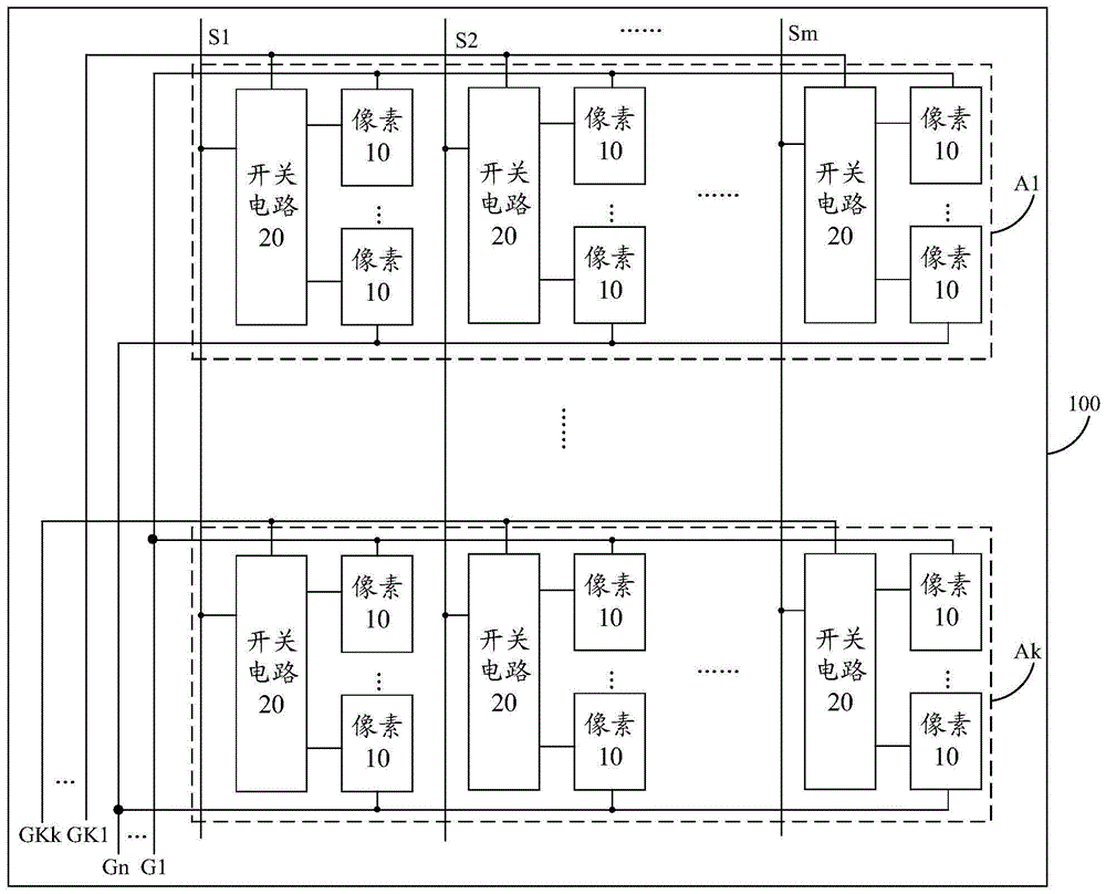
The embodiment of the disclosure provides an array substrate, which can realize the line-by-line reliable scanning of a plurality of lines of pixels on the premise of effectively reducing the number of grid lines required to be arranged in the array substrate, and is beneficial to the design of a narrow frame. Fig. 2 is a schematic structural diagram of an array substrate according to an embodiment of the present disclosure. As shown in fig. 2, the array substrate 100 has a plurality of partitions a. The array substrate 100 may include: a plurality of data lines S, a plurality of first gate lines GK, a plurality of second gate lines G, and a plurality of pixels 10 and a plurality of switching circuits 20 at each partition a.
For example, referring to fig. 2, which shows an array substrate 100 having k divisional areas A1 to Ak, the array substrate 100 is shown to include m data lines S1 to Sm, k first gate lines GK1 to GKk, n second gate lines G1 to Gn, and n rows and m columns of pixels 10 and m switching circuits 20 located in each divisional area a and arranged in an array. Alternatively, the number of pixel rows in different partitions a may not be equal.
Wherein each of the first gate lines GK may be connected to a plurality of switching circuits 20 located in at least one division a. Each of the first gate lines GK may provide a first gate driving signal to the switching circuit 20 to which it is connected.
Each data line S may be connected to a plurality of switch circuits 20 located in the same column. Each data line S may provide a data signal to the switching circuit 20 to which it is connected.
Each switching circuit 20 may also be connected to a column of pixels 10 of the partition a in which it is located. Each of the switching circuits 20 may output a data signal to a column of the pixels 10 to which it is connected in response to the first gate driving signal.
For example, each of the switching circuits 20 may output a data signal supplied from the data line S to a column of the pixels 10 to which it is connected when the first gate line GK supplies the first gate driving signal thereto.
Each second gate line G may be connected to a plurality of rows of pixels 10, and at least two rows of pixels 10 connected to each second gate line G are located in different partitions a. Each second gate line G may provide a second gate driving signal to the plurality of rows of pixels 10 to which it is connected.
For example, each pixel 10 may emit light when the second gate line G supplies a second gate driving signal thereto, and the switching circuit 20 connected thereto outputs a data signal thereto in response to the first gate driving signal.
In summary, the embodiment of the present disclosure provides an array substrate, which includes a plurality of data lines, a plurality of first gate lines, a plurality of second gate lines, a plurality of pixels, and a plurality of switch circuits. Since each first gate line is connected to a plurality of switching circuits located in at least one partition, and each switching circuit is connected to a column of pixels in the partition where it is located, each switching circuit can output a data signal to the column of pixels to which it is connected in response to a gate driving signal supplied from the first gate line, one second gate line may be provided to be connected to a plurality of rows of pixels located in different partitions. Reliable scanning of a plurality of rows of pixels row by row can be ensured by flexible control of the signals provided by the signal lines. That is, on the premise of ensuring the driving reliability, the number of the grid lines required to be arranged is effectively reduced, and the narrow frame design is facilitated.
Fig. 3 is a schematic structural diagram of another array substrate provided in an embodiment of the present disclosure. As shown in fig. 3, each first gate line GK may be connected to a plurality of switch circuits 20 of one partition a, and the switch circuits 20 connected to each first gate line GK are located in different partitions a.
For example, referring to fig. 3, the array substrate 100 has k partitions A1 to Ak, where k is a positive integer greater than 1. Correspondingly, the array substrate 100 may include k first gate lines GK1 to GKk. Wherein the first gate line GK1 can be connected to the plurality of switch circuits 20 located in the first sub-area A1, the second gate line GK2 can be connected to the plurality of switch circuits 20 located in the second sub-area A2, and so on, the kth first gate line GKk can be connected to the plurality of switch circuits 20 located in the kth sub-area Ak.
By providing each first gate line GK to be connected to only the plurality of switching circuits 20 located in one division a, it is possible to make each first gate line GK independently control the operating states of only the plurality of pixels 10 located in one division a. In addition, by arranging each first gate line GK to be connected to a plurality of switch circuits 20 located in different partitions a, sequential scanning of each partition can be realized by flexibly controlling the driving signals provided by each first gate line GK, and the display effect can be ensured. For example, when the first gate driving signals are sequentially supplied to the k first gate lines GK1 to GKk, the switching circuits 20 in the k partitions a are sequentially turned on, and the pixels in the k partitions a sequentially emit light.
Alternatively, referring to fig. 3, each row of pixels 10 connected to each second gate line G may be located in a different partition a. That is, each second gate line G may be connected to a plurality of rows of pixels 10 located in different partitions a. And, the pixels 10 connected by each second gate line G are located in different rows. For example, assuming that each second gate line G connects 100 rows of pixels 10 in common, the 100 rows of pixels 10 may all be located in different partitions a.
By setting each first gate line Gk to be connected to a plurality of switch circuits 20 located in one partition a and setting each second gate line G to be connected to a plurality of rows of pixels 10 located in a different partition a, it is possible to further prevent a plurality of rows of pixels located in the same partition a from emitting light at the same time by flexibly adjusting the second gate driving signal provided by the second gate line G, i.e., it is possible to further secure a display effect.
Alternatively, referring to fig. 3, the array substrate 100 may include n second gate lines G1 to Gn, and each of the partitions a may include n rows of pixels 10. The ith second gate line Gi may be connected to the ith row of pixels 10 of each partition a, n is a positive integer greater than 1, and i is a positive integer less than or equal to n. That is, every two adjacent rows of pixels 10 connected by each second gate line G have the same number of pixel rows.
For example, referring to fig. 3, when i is equal to 1, the first second gate line G1 may be connected to the first row of pixels 10 in each partition a, when i is equal to 2, the second gate line G2 may be connected to the second row of pixels 10 in each partition a, and so on, and when i is equal to n, the nth second gate line Gn may be connected to the nth row of pixels 10 in each partition a.
The ith second grid line G is connected with the ith row of pixels 10 of each subarea A, so that the arrangement of the second grid lines G is facilitated, and when grid driving signals are sequentially provided for the plurality of second grid lines G, the plurality of rows of pixels 10 in each subarea A can sequentially emit light along the extending direction of the data line S, and the display effect of the array substrate is further ensured.
Optionally, fig. 4 is a schematic structural diagram of another array substrate provided in the embodiment of the present disclosure. As shown in fig. 4, each pixel 10 may include a driving transistor T1 and a light emitting element L1, and each switching circuit 20 may include: the transistor K1 is switched.
As can be seen from fig. 3 and 4, the gate electrode of the switching transistor K1 may be connected to the first gate line GK, the first pole of the switching transistor K1 may be connected to the data line S, and the second pole of the switching transistor K1 may be connected to the first pole of the driving transistor T1.
The gate electrode of the driving transistor T1 may be connected to the second gate line G, and the second electrode of the driving transistor T1 may be connected to the light emitting element L1.
Alternatively, the array substrate 100 may be an array substrate of an LCD display device, or an array substrate of an Organic Light-Emitting Diode (OLED) display device.
Referring to fig. 4, when the array substrate is an array substrate of an LCD display device, the light emitting element L1 may include a pixel electrode, a common electrode, and liquid crystal molecules between the pixel electrode and the common electrode. Referring to fig. 4, the pixel electrode and the common electrode may be equivalent to a liquid crystal capacitor Clc, and a storage capacitor Cst may be formed between the pixel electrode and the common electrode. The second electrode of the driving transistor T1 may be connected to the pixel electrode of the light emitting element L1. Alternatively, as can also be seen in fig. 3 and 4, the array substrates 100 shown therein each include m data lines S1 to Sm.
Alternatively, each of the switching circuits 20 may be located in a non-display region of one pixel 10, or each of the switching circuits 20 may be located in a region between two adjacent pixels 10. That is, each switching transistor K1 connected to the first gate line GK may be laid out within the pixel 10, or may be laid out outside the pixel 10 as needed. In addition, the driving transistor T1 connected to the second gate line G may be laid out within the pixel 10.
Alternatively, referring to fig. 3 and 4, each first gate line GK may include a first sub-line segment GK01 and a second sub-line segment GK02, and each second gate line G may include a third sub-line segment G01 and a fourth sub-line segment G02.
Each of the first sub-line segments GK01 and each of the third sub-line segments G01 may be parallel to each other, and may both be perpendicular to the extending direction of the data line S. Each of the second sub-line segments GK02 and each of the fourth sub-line segments G02 may be parallel to each other, and may be parallel to the extending direction of the data line S. That is, two sub-line segments included in each first gate line GK may be perpendicular to each other, and two sub-line segments included in each second gate line G may also be perpendicular to each other.
Accordingly, assuming that the array substrate 100 has k partitions, each partition k includes n rows of pixels, when k is greater than 1,n is greater than 2, comparing fig. 1, 3 and 4 can obtain: the array substrate in the related art needs to provide k × n gate lines to drive the plurality of rows of pixels 10 in the array substrate 100, and correspondingly, the peripheral routing fan-out region of the array substrate 100 in the related art needs to provide a portion of line segments of the k × n gate lines. The array substrate provided by the embodiment of the present disclosure can realize reliable scanning of the plurality of rows of pixels 10 in the array substrate 100 only by setting k + n gate lines, and accordingly, the peripheral routing fan-out area of the array substrate 100 provided by the embodiment of the present disclosure only needs to set a part of line segments of the k + n gate lines. That is, the number of signal lines required to be arranged in the peripheral routing fan-out area of the array substrate provided by the embodiment of the disclosure is small, which is beneficial to narrow frame design.
In summary, the embodiment of the present disclosure provides an array substrate, which includes a plurality of data lines, a plurality of first gate lines, a plurality of second gate lines, a plurality of pixels, and a plurality of switch circuits. Since each first gate line is connected to a plurality of switching circuits located in at least one partition, and each switching circuit is connected to a column of pixels in the partition where it is located, each switching circuit can output a data signal to the column of pixels to which it is connected in response to a gate driving signal supplied from the first gate line, one second gate line may be provided to be connected to a plurality of rows of pixels located in different partitions. Reliable scanning of a plurality of rows of pixels row by row can be ensured by flexible control of the signals provided by the signal lines. That is, on the premise of ensuring the driving reliability, the number of the grid lines required to be arranged is effectively reduced, and the narrow frame design is facilitated.
Fig. 5 is a flowchart of a driving method of an array substrate according to an embodiment of the present disclosure, which can be applied to the array substrate shown in any one of fig. 2 to 4. As shown in fig. 5, the method may include:
step 501, in a signal writing stage, sequentially providing a first gate driving signal to a plurality of first gate lines, providing a data signal to each data line, and sequentially providing a second gate driving signal to a plurality of second gate lines, wherein the switching circuit outputs the data signal to a row of pixels connected to the switching circuit in response to the first gate driving signal.
And sequentially providing a second gate driving signal to the plurality of second gate lines within a time period of providing the first gate driving signal to each first gate line.
In summary, the embodiments of the present disclosure provide a driving method of an array substrate. The switching circuit can respond to the first grid driving signal provided by the first grid line and output a data signal to a column of pixels connected with the first grid line, so that only one second grid line can be arranged to be connected with a plurality of rows of pixels positioned in different subareas, and the row-by-row reliable scanning of the plurality of rows of pixels can be ensured by flexibly controlling the signals provided by the signal lines by adopting the driving method. Under the prerequisite that effectively reduces the grid line quantity that needs set up promptly, guaranteed the drive reliability, be favorable to narrow frame design.
Optionally, referring to fig. 5, after the signal writing phase, that is, after the step 501, the method may further include: step 502, a first holding stage, sequentially providing a second gate driving signal to the plurality of second gate lines, and stopping providing the first gate driving signal to each first gate line.
Accordingly, in the first holding stage, the driving transistors connected to the plurality of second gate lines may be sequentially turned on and sequentially turned off, and the switching transistors connected to the plurality of first gate lines may be kept in a turned-off state. By performing this first holding stage, the problem of characteristic drift of the driving transistor due to the long-term maintenance of negative or positive voltage can be avoided, thereby achieving low-frequency (e.g., 1 hz) driving.
Step 503, a second holding stage, sequentially providing the first gate driving signal to each first gate line, and stopping providing the second gate driving signal to each second gate line.
Correspondingly, in the second holding stage, the switching transistors connected to each first gate line may be sequentially turned on, sequentially turned off, sequentially turned on, and sequentially turned off for continuous cycle execution, and the driving transistors connected to the plurality of second gate lines may be kept in a turned-off state. By performing this second holding phase, the problem of characteristic drift of the switching transistor due to maintaining a negative or positive voltage for a long time can be avoided.
It should be noted that the signal writing phase, the first holding phase and the second holding phase may be performed within a frame scanning time, and the signal writing phase, the first holding phase and the second holding phase may be sequentially performed every frame scanning. I.e., each frame scan, can refer to the driving method shown in fig. 5.
It should be further noted that the sequence of the steps of the driving method of the array substrate provided in the embodiment of the present disclosure may be appropriately adjusted, and the steps may also be increased or decreased according to the situation. For example, the step 503 may be performed before the step 502, that is, after the signal writing phase, the second holding phase is performed first and then the first holding phase is performed. Alternatively, the above-mentioned step 502 or step 503 may be deleted as the case may be, i.e., only the first holding phase or only the second holding phase may be performed after the signal writing phase. Any method that can be easily conceived by those skilled in the art within the technical scope of the present disclosure is covered by the protection scope of the present invention, and thus, the detailed description thereof is omitted.
Taking the array substrate shown in fig. 4 as an example, and taking the driving transistor and the switching transistor as N-type transistors, providing the gate driving signal is equivalent to providing the gate driving signal at the first potential, stopping providing the gate driving signal is equivalent to providing the gate driving signal at the second potential, and the first potential is a high potential with respect to the second potential, the driving principle of the array substrate provided by the embodiment of the disclosure is described:
fig. 6 is a timing diagram of signals output to the signal lines according to an embodiment of the disclosure. As shown in fig. 6, in the signal writing stage t1, a first gate driving signal may be sequentially supplied to the first to kth first gate lines GK1 to GKk. That is, when the first gate driving signal at the first potential is supplied to one first gate line GK, the first gate driving signal at the second potential is supplied to all the other first gate lines GK except the first gate line GK. Correspondingly, the m switch transistors K1 located in the first partition A1 to the m switch transistors K1 located in the kth partition Ak may be sequentially turned on, and the m switch transistors K1 located in the same partition a may be simultaneously turned on. The data lines S1 to Sm may output data signals to the driving transistor T1 to which each switching transistor K1 is connected through m switching transistors K1.
Also, referring to fig. 6, during a period of time in which the first gate driving signal is supplied to one first gate line GK, the second gate driving signal may be sequentially supplied to the first to nth second gate lines G1 to Gn. That is, when the second gate driving signal at the first potential is supplied to one second gate line G1, the second gate driving signal at the second potential is supplied to all the other second gate lines G except the second gate line G. Accordingly, the driving transistors T1 of the n rows of pixels 10 in one partition a controlled by the first gate line GK may be turned on row by row, and the driving transistors T1 of the m pixels 10 in the same row may be turned on simultaneously. The data signal can be output to the pixel electrode connected to the m driving transistors T1 through the turned-on m driving transistors T1 to charge the pixel electrode, so that the liquid crystal molecules are deflected and the pixel emits light.
For example, taking the first gate driving signal at the first potential provided to the first gate line GK1 as an example, the first gate driving signal at the second potential is provided to the second to kth first gate lines GK2 to GKk. The m switching transistors K1 located in the first partition A1 are all turned on, and the switching transistors K1 located in the second partition A2 to the kth partition Ak are all turned off. At this time, the data lines S1 to Sm may output data signals to the driving transistors T1 of the n rows and m columns of pixels 10 located in the first partition A1 through the m switching transistors K1 located in the first partition A1.
At this time, the second gate driving signal at the first potential is sequentially supplied to the first to nth second gate lines G1 to Gn, and the driving transistors T1 in the first to nth rows of pixels 10 in the respective partitions a are turned on row by row. For example, when the first gate line G1 supplies the second gate driving signal at the first potential, the driving transistors T1 in the m pixels 10 of the first row in each division are turned on. Since the data lines S1 to Sm output data signals only to the plurality of driving transistors T1 located in the first partition A1, at this time, the data signals are output to the pixel electrodes of the plurality of rows of pixels located in the first partition A1 row by row only through the driving transistors T1 located in the first partition A1 row by row, and the charging of the liquid crystal capacitor Clc and the storage capacitor Cst is achieved. Starting from the first row of pixels 10 located in the first partition A1, the line-by-line charging of the n rows of pixels is sequentially realized.
After the pixels in the first sub-area A1 are charged, the first gate driving signal at the first potential is provided to the second first gate line GK2, and the second gate driving signal at the first potential is provided to the first second gate line G1 to the nth second gate line Gn again in sequence, so that the progressive scanning of the n rows of pixels in the second sub-area A2 is realized. And repeating the steps until the n lines of pixels in the k-th partition Ak are scanned line by line, so that the updating of one frame of picture is realized. This driving method may also be referred to as sector scanning.
In the first hold phase t2, the second gate driving signal at the first potential is sequentially provided to the first to nth second gate lines G1 to Gn, and the first gate driving signal at the first potential is stopped being provided to the first to kth first gate lines GK1 to GKk, that is, the first gate driving signal at the second potential is provided to the first to kth first gate lines GK1 to GKk. Correspondingly, the plurality of switching transistors K1 included in the array substrate 100 are all turned off, and the driving transistors T1 of the pixels 10 in each row in each partition a are sequentially turned on and sequentially turned off. Since the pixel can be driven to emit light only when the first gate driving signal and the second gate driving signal are provided, the pixel is not charged in the first holding period t2, and the problem of characteristic drift caused by the driving transistor maintaining the negative voltage for a long time can be effectively solved by executing the driving method of the first holding period t 2.
In the second holding period t3, the first gate driving signal at the first potential is sequentially supplied to each first gate line GK, and the supply of the second gate driving signal to the first to nth second gate lines G1 to Gn is stopped, that is, the second gate driving signal at the second potential is supplied to each second gate line G. Accordingly, the plurality of switching transistors K1 in each partition a are cyclically turned on and off, and the driving transistors T1 of the pixels 10 in each row in each partition a are kept off. Similarly, since the pixel can be driven to emit light only when the first gate driving signal and the second gate driving signal are provided, the pixel is not charged in the second holding period t3, and the problem of characteristic drift caused by long-time maintaining of the negative voltage of the on transistor can be effectively solved by executing the second holding period t3.
It should be noted that the execution sequence of the first holding phase t2 and the second holding phase t3 is not limited, and as shown in fig. 6, the first holding phase t2 may be executed first, and then the second holding phase t3 may be executed. Alternatively, as shown in fig. 7, the second holding phase t3 may be performed before the first holding phase t1 is performed after the signal writing phase t1. The embodiments of the present disclosure do not limit this.
It should be noted that, in conjunction with fig. 6 and fig. 7, the first holding phase t2 and the second holding phase t3 may be collectively referred to as a holding phase, that is, each frame update includes two phases, namely a signal writing phase and a holding phase. The duration of supplying the first gate driving signal at the first potential to the first gate line Gk is the charging time for charging the pixels in one partition a, and the duration of supplying the second gate driving signal at the first potential to the second gate line G is the charging time for charging the pixels in one row.
In summary, the embodiments of the present disclosure provide a driving method of an array substrate. Because the switching circuit can respond to the first grid driving signal provided by the first grid line and output a data signal to a column of pixels connected with the first grid line, only one second grid line can be arranged to be connected with a plurality of rows of pixels positioned in different subareas, and the row-by-row reliable scanning of the plurality of rows of pixels can be ensured by flexibly controlling the signals provided by the signal lines by adopting the driving method. Under the prerequisite that effectively reduces the grid line quantity that needs set up promptly, guaranteed the drive reliability, be favorable to narrow frame design.
Fig. 8 is a schematic structural diagram of a display module according to an embodiment of the disclosure. As shown in fig. 8, the display module may include: a gate driving circuit 01, a source driving circuit 02, and an array substrate 100 as shown in any one of fig. 2 to 4.
The gate driving circuit 01 may be connected to a first gate line GK and a second gate line G in the array substrate 100, and the gate driving circuit 01 is configured to provide a first gate driving signal to the first gate line GK and provide a second gate driving signal to the second gate line G. The source driving circuit 02 may be connected to the data lines S in the array substrate 100, and the source driving circuit 02 may be used to provide data signals to the data lines S.
For example, referring to fig. 8, the array substrate 100 shown includes k first gate lines GK1 to GKk, n second gate lines G1 to Gn, and m data lines S1 to Sm. Referring to fig. 8, the gate driving circuit 01 may be connected to the k first gate lines GK1 to GKk and the n second gate lines G1 to Gn, and the source driving circuit 02 may be connected to the m data lines S1 to Sm.
Optionally, the gate driving circuit 01 may include: the first grid driving chip and the second grid driving chip. The first gate driving chip may be connected to the first gate line GK, and configured to provide a first gate driving signal to the first gate line GK; the second gate driving chip may be connected to the second gate line G for providing a second gate driving signal to the second gate line G. The first gate driving chip may also be referred to as a primary gate driving circuit, and the second gate driving chip may also be referred to as a secondary gate driving circuit.
Optionally, the embodiment of the disclosure further provides a display device. The display device may include: such as the display module shown in fig. 8. The display device may be: any product or component with a display function, such as an LCD display device, electronic paper, an OLED display device, an AMOLED display device, electronic paper, an electrowetting display device, a mobile phone, a television, a display, a notebook computer, a digital photo frame, and a navigator.
It can be clearly understood by those skilled in the art that, for convenience and brevity of description, the specific working processes of the array substrate and each circuit described above may refer to the corresponding processes in the foregoing method embodiments, and are not described herein again.
The above description is intended to be exemplary only and not to limit the present disclosure, and any modification, equivalent replacement, or improvement made without departing from the spirit and scope of the present disclosure is to be considered as the same as the present disclosure.