CN112946966A - Large-angle liquid crystal optical phased array scanning assembly - Google Patents

Large-angle liquid crystal optical phased array scanning assembly Download PDF

Info

Publication number
CN112946966A
CN112946966A CN202110147899.XA CN202110147899A CN112946966A CN 112946966 A CN112946966 A CN 112946966A CN 202110147899 A CN202110147899 A CN 202110147899A CN 112946966 A CN112946966 A CN 112946966A
Authority
CN
China
Prior art keywords
liquid crystal
phased array
cholesteric liquid
laser
optical phased
Prior art date
Legal status (The legal status is an assumption and is not a legal conclusion. Google has not performed a legal analysis and makes no representation as to the accuracy of the status listed.)
Granted
Application number
CN202110147899.XA
Other languages
Chinese (zh)
Other versions
CN112946966B (en
Inventor
汪相如
梁知清
贺晓娴
Current Assignee (The listed assignees may be inaccurate. Google has not performed a legal analysis and makes no representation or warranty as to the accuracy of the list.)
Huzhou Tongmu Information Technology Service Co ltd
Original Assignee
University of Electronic Science and Technology of China
Priority date (The priority date is an assumption and is not a legal conclusion. Google has not performed a legal analysis and makes no representation as to the accuracy of the date listed.)
Filing date
Publication date
Application filed by University of Electronic Science and Technology of China filed Critical University of Electronic Science and Technology of China
Priority to CN202110147899.XA priority Critical patent/CN112946966B/en
Publication of CN112946966A publication Critical patent/CN112946966A/en
Application granted granted Critical
Publication of CN112946966B publication Critical patent/CN112946966B/en
Active legal-status Critical Current
Anticipated expiration legal-status Critical

Links

Images

Classifications

    • GPHYSICS
    • G02OPTICS
    • G02FOPTICAL DEVICES OR ARRANGEMENTS FOR THE CONTROL OF LIGHT BY MODIFICATION OF THE OPTICAL PROPERTIES OF THE MEDIA OF THE ELEMENTS INVOLVED THEREIN; NON-LINEAR OPTICS; FREQUENCY-CHANGING OF LIGHT; OPTICAL LOGIC ELEMENTS; OPTICAL ANALOGUE/DIGITAL CONVERTERS
    • G02F1/00Devices or arrangements for the control of the intensity, colour, phase, polarisation or direction of light arriving from an independent light source, e.g. switching, gating or modulating; Non-linear optics
    • G02F1/01Devices or arrangements for the control of the intensity, colour, phase, polarisation or direction of light arriving from an independent light source, e.g. switching, gating or modulating; Non-linear optics for the control of the intensity, phase, polarisation or colour 
    • G02F1/13Devices or arrangements for the control of the intensity, colour, phase, polarisation or direction of light arriving from an independent light source, e.g. switching, gating or modulating; Non-linear optics for the control of the intensity, phase, polarisation or colour  based on liquid crystals, e.g. single liquid crystal display cells
    • G02F1/137Devices or arrangements for the control of the intensity, colour, phase, polarisation or direction of light arriving from an independent light source, e.g. switching, gating or modulating; Non-linear optics for the control of the intensity, phase, polarisation or colour  based on liquid crystals, e.g. single liquid crystal display cells characterised by the electro-optical or magneto-optical effect, e.g. field-induced phase transition, orientation effect, guest-host interaction or dynamic scattering
    • G02F1/13718Devices or arrangements for the control of the intensity, colour, phase, polarisation or direction of light arriving from an independent light source, e.g. switching, gating or modulating; Non-linear optics for the control of the intensity, phase, polarisation or colour  based on liquid crystals, e.g. single liquid crystal display cells characterised by the electro-optical or magneto-optical effect, e.g. field-induced phase transition, orientation effect, guest-host interaction or dynamic scattering based on a change of the texture state of a cholesteric liquid crystal
    • GPHYSICS
    • G02OPTICS
    • G02FOPTICAL DEVICES OR ARRANGEMENTS FOR THE CONTROL OF LIGHT BY MODIFICATION OF THE OPTICAL PROPERTIES OF THE MEDIA OF THE ELEMENTS INVOLVED THEREIN; NON-LINEAR OPTICS; FREQUENCY-CHANGING OF LIGHT; OPTICAL LOGIC ELEMENTS; OPTICAL ANALOGUE/DIGITAL CONVERTERS
    • G02F1/00Devices or arrangements for the control of the intensity, colour, phase, polarisation or direction of light arriving from an independent light source, e.g. switching, gating or modulating; Non-linear optics
    • G02F1/01Devices or arrangements for the control of the intensity, colour, phase, polarisation or direction of light arriving from an independent light source, e.g. switching, gating or modulating; Non-linear optics for the control of the intensity, phase, polarisation or colour 
    • G02F1/13Devices or arrangements for the control of the intensity, colour, phase, polarisation or direction of light arriving from an independent light source, e.g. switching, gating or modulating; Non-linear optics for the control of the intensity, phase, polarisation or colour  based on liquid crystals, e.g. single liquid crystal display cells
    • G02F1/133Constructional arrangements; Operation of liquid crystal cells; Circuit arrangements
    • G02F1/1333Constructional arrangements; Manufacturing methods
    • G02F1/1335Structural association of cells with optical devices, e.g. polarisers or reflectors
    • G02F1/13363Birefringent elements, e.g. for optical compensation
    • GPHYSICS
    • G02OPTICS
    • G02FOPTICAL DEVICES OR ARRANGEMENTS FOR THE CONTROL OF LIGHT BY MODIFICATION OF THE OPTICAL PROPERTIES OF THE MEDIA OF THE ELEMENTS INVOLVED THEREIN; NON-LINEAR OPTICS; FREQUENCY-CHANGING OF LIGHT; OPTICAL LOGIC ELEMENTS; OPTICAL ANALOGUE/DIGITAL CONVERTERS
    • G02F1/00Devices or arrangements for the control of the intensity, colour, phase, polarisation or direction of light arriving from an independent light source, e.g. switching, gating or modulating; Non-linear optics
    • G02F1/01Devices or arrangements for the control of the intensity, colour, phase, polarisation or direction of light arriving from an independent light source, e.g. switching, gating or modulating; Non-linear optics for the control of the intensity, phase, polarisation or colour 
    • G02F1/13Devices or arrangements for the control of the intensity, colour, phase, polarisation or direction of light arriving from an independent light source, e.g. switching, gating or modulating; Non-linear optics for the control of the intensity, phase, polarisation or colour  based on liquid crystals, e.g. single liquid crystal display cells
    • G02F1/133Constructional arrangements; Operation of liquid crystal cells; Circuit arrangements
    • G02F1/1333Constructional arrangements; Manufacturing methods
    • G02F1/1343Electrodes
    • GPHYSICS
    • G02OPTICS
    • G02FOPTICAL DEVICES OR ARRANGEMENTS FOR THE CONTROL OF LIGHT BY MODIFICATION OF THE OPTICAL PROPERTIES OF THE MEDIA OF THE ELEMENTS INVOLVED THEREIN; NON-LINEAR OPTICS; FREQUENCY-CHANGING OF LIGHT; OPTICAL LOGIC ELEMENTS; OPTICAL ANALOGUE/DIGITAL CONVERTERS
    • G02F1/00Devices or arrangements for the control of the intensity, colour, phase, polarisation or direction of light arriving from an independent light source, e.g. switching, gating or modulating; Non-linear optics
    • G02F1/29Devices or arrangements for the control of the intensity, colour, phase, polarisation or direction of light arriving from an independent light source, e.g. switching, gating or modulating; Non-linear optics for the control of the position or the direction of light beams, i.e. deflection
    • G02F1/292Devices or arrangements for the control of the intensity, colour, phase, polarisation or direction of light arriving from an independent light source, e.g. switching, gating or modulating; Non-linear optics for the control of the position or the direction of light beams, i.e. deflection by controlled diffraction or phased-array beam steering

Landscapes

  • Physics & Mathematics (AREA)
  • Nonlinear Science (AREA)
  • General Physics & Mathematics (AREA)
  • Optics & Photonics (AREA)
  • Chemical & Material Sciences (AREA)
  • Crystallography & Structural Chemistry (AREA)
  • Mathematical Physics (AREA)
  • Liquid Crystal (AREA)

Abstract

本发明公开了一种大角度液晶光学相控阵扫描组件,包括激光器、四分之一波片、光波导、胆甾相液晶器件和液晶光学相控阵;激光器出射的激光经过四分之一波片后耦合进入光波导,沿光波导传播;所述光波导呈弧形结构,光波导的内侧设有金属反射层,外侧设有ITO膜层;ITO膜层的外侧设有多个胆甾相液晶器件,胆甾相液晶器件的外侧依次设有ITO电极、四分之一波片和液晶光学相控阵;胆甾相液晶器件用于作为激光透射或者反射的选择开关。本发明通过胆甾相液晶单元器件的选择,波导中的激光将反射或者透射至液晶光学相控阵,实现了控制扫描;采用多个胆甾相液晶单元器件以及多个液晶光学相控阵,能够实现大角度扫描。

Figure 202110147899

The invention discloses a large-angle liquid crystal optical phased array scanning component, comprising a laser, a quarter wave plate, an optical waveguide, a cholesteric liquid crystal device and a liquid crystal optical phased array; The wave plate is then coupled into the optical waveguide and propagates along the optical waveguide; the optical waveguide has an arc structure, the inner side of the optical waveguide is provided with a metal reflective layer, and the outer side is provided with an ITO film layer; the outer side of the ITO film layer is provided with a plurality of cholesteric layers The cholesteric liquid crystal device is provided with an ITO electrode, a quarter-wave plate and a liquid crystal optical phased array in sequence on the outside of the cholesteric liquid crystal device; the cholesteric liquid crystal device is used as a selection switch for laser transmission or reflection. Through the selection of cholesteric liquid crystal cell devices, the laser in the waveguide will be reflected or transmitted to the liquid crystal optical phased array to realize controlled scanning; multiple cholesteric liquid crystal cell devices and multiple liquid crystal optical phased arrays are used, Able to achieve wide angle scanning.

Figure 202110147899

Description

Large-angle liquid crystal optical phased array scanning assembly
Technical Field
The invention belongs to the technical field of liquid crystal optical phased array technology and liquid crystal optoelectronic devices, and particularly relates to a large-angle liquid crystal optical phased array scanning assembly.
Background
The light beam deflection scanning technology is widely applied to the fields of laser communication, target tracking and the like. The control method of the laser scanning at home and abroad at present is mainly divided into a mechanical type and a non-mechanical type, the mechanical deflection realizes the beam deflection by changing the direction of an optical axis by a mechanical device, the response is slow, the scanning has the defects of mechanical inertia, large device volume, high manufacturing cost and the like; with the continuous and deep research and the mature manufacturing process of the non-mechanical beam deflection technology, the Liquid Crystal Optical Phased Array (LCOPA) technology becomes a research hotspot, and the LCOPA has the advantages of no inertia, high scanning precision, low SWaP (size, weight and power consumption) and the like, and is an important research direction in beam deflection.
The liquid crystal optical phased array technology overcomes many defects of the mechanical deflection technology, but the liquid crystal optical phased array technology also faces the problem of narrow beam scanning range (about +/-3 degrees), and is mainly influenced by the array size of a liquid crystal box, the phase modulation depth and the current process technology. At present, the large-angle scanning mode adopts a cascade technology, the cost consumption caused by device cascade is large, and the insertion loss is large due to the fact that a plurality of layers of light beams pass through the cascade. As the industrial application is promoted, the manufacturing process of the liquid crystal device is very mature, and therefore, the realization of a large beam deflection range and low manufacturing cost is an urgent problem to be solved in the field.
Disclosure of Invention
The invention aims to overcome the defects of the prior art and provide a large-angle liquid crystal optical phased array scanning component which realizes control scanning by selecting cholesteric liquid crystal single elements and reflecting or transmitting laser in a waveguide to a liquid crystal optical phased array and realizes large-angle scanning by adopting a plurality of cholesteric liquid crystal single elements and a plurality of liquid crystal optical phased arrays.
The purpose of the invention is realized by the following technical scheme: a large-angle liquid crystal optical phased array scanning assembly comprises a laser, a quarter-wave plate, an optical waveguide, a cholesteric liquid crystal device and a liquid crystal optical phased array; laser emitted by the laser device is coupled into the optical waveguide after passing through the quarter-wave plate and is transmitted along the optical waveguide; the optical waveguide is of an arc-shaped structure, a metal reflecting layer is arranged on the inner side of the optical waveguide, and an ITO film layer is arranged on the outer side of the optical waveguide; a plurality of cholesteric liquid crystal devices are arranged on the outer side of the ITO film layer, and ITO electrodes, quarter-wave plates and liquid crystal optical phased arrays are sequentially arranged on the outer side of the cholesteric liquid crystal devices; cholesteric liquid crystal devices are used as selective switches for laser transmission or reflection.
Further, the optical axis of the quarter-wave plate positioned between the cholesteric liquid crystal device and the liquid crystal optical phased array is consistent with the direction of the optical axis of the adjacent liquid crystal optical phased array.
Further, when the cholesteric liquid crystal device is in a non-power-on state, the relation between the screw pitch and the laser wavelength is as follows:
Figure BDA0002930925130000021
lambda is the wavelength of the laser light,
Figure BDA0002930925130000022
is the average refractive index in a plane perpendicular to the helical axis, thetaiAngle of incidence of the laser, θsThe reflection angle of the laser is shown, and p is the screw pitch of the cholesteric liquid crystal;
the handedness of the cholesteric liquid crystal device coincides with the handedness of the laser.
Further, the cholesteric liquid crystal device comprises two layers of electrodes, wherein the upper layer of electrodes are a common electrode and are adjacent to the ITO film layer; the lower electrode is a discrete conductive area and is adjacent to the quarter-wave plate;
the reflection and transmission properties of cholesteric liquid crystal devices are modified by writing voltages on the upper and lower layer electrodes: when the upper and lower layers of electrodes of the cholesteric liquid crystal device are not electrified, the rotating direction of the cholesteric liquid crystal device is consistent with the rotating direction of the laser in the optical waveguide, and the cholesteric liquid crystal device reflects the incident laser; when the upper and lower electrodes of the cholesteric liquid crystal device are electrified, the thread pitch of the cholesteric liquid crystal device is completely untied, the liquid crystal texture is completely changed into a field nematic phase, the reflectivity is zero, the Bragg reflection effect disappears, and the incident laser is transmitted.
Furthermore, the liquid crystal optical phased array, the quarter-wave plate adjacent to the liquid crystal optical phased array and the ITO electrode are all located at the center of the lower layer electrode of the cholesteric liquid crystal device, and the width of the ITO electrode is larger than the reflection period L of one laser and smaller than the reflection period 2L of two lasers.
The invention has the beneficial effects that: the cholesteric liquid crystal pitch design of the invention ensures that the reflection wavelength is consistent with the laser wavelength in the waveguide, when laser transmission is needed, certain voltage is applied to cholesteric liquid crystal to ensure that the uncoiling of the cholesteric liquid crystal is completely changed into field nematic phase, the cholesteric liquid crystal no longer has Bragg reflection effect, the reflectivity is zero, the laser in the waveguide realizes transmission, and the cholesteric liquid crystal enters the liquid crystal optical phased array device after the laser transmission and is controlled to be scanned with precision. According to the invention, through the selection of the cholesteric liquid crystal single element, laser in the waveguide is reflected or transmitted to the liquid crystal optical phased array, so that control scanning is realized; by adopting a plurality of cholesteric liquid crystal single elements and a plurality of liquid crystal optical phased arrays, large-angle scanning can be realized, and the problems that in the prior art, the field range of a single liquid crystal optical phased array is narrow, the cost of the prior cascading technology is high, the insertion loss is large and the like are solved.
Drawings
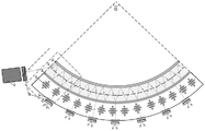
FIG. 1 is a first schematic structural diagram of a wide angle liquid crystal optical phased array scanning assembly according to the present invention;
FIG. 2 is a second schematic diagram of a large angle liquid crystal optical phased array scanning assembly according to the present invention;
FIG. 3 is a schematic diagram of a liquid crystal optical phased array of the present invention;
description of reference numerals: the liquid crystal display comprises a 1-laser, a 2-metal reflecting layer, a 3-optical waveguide, a 4-ITO film layer, a 5-cholesteric phase liquid crystal device, a 6-ITO electrode, a 7-liquid crystal optical phased array, an 8-quarter wave plate, 9-quartz glass, a 10-ITO film layer, an 11-ITO electrode, a 12-PI orientation layer, a 13-spacer and a 14-liquid crystal.
Detailed Description
The technical scheme of the invention is further explained by combining the attached drawings.
As shown in fig. 1, the large-angle liquid crystal optical phased array scanning assembly of the present invention includes a laser 1, a quarter wave plate, an optical waveguide 3, a cholesteric liquid crystal device 5 and a liquid crystal optical phased array 7; laser emitted by the laser 1 is coupled into the optical waveguide 3 after passing through the quarter-wave plate and is transmitted along the optical waveguide; the optical waveguide 3 is of an arc-shaped structure, the inner side of the optical waveguide 3 is provided with a metal reflecting layer 2, and the outer side of the optical waveguide is provided with an ITO film layer 4; a plurality of cholesteric liquid crystal devices 5 are arranged on the outer side of the ITO film layer 4, and ITO electrodes 6, quarter-wave plates and a liquid crystal optical phased array 7 are sequentially arranged on the outer side of the cholesteric liquid crystal devices 5; the cholesteric liquid crystal device 5 is used as a selection switch for transmission or reflection of laser light.
Further, the optical axis of the quarter-wave plate positioned between the cholesteric liquid crystal device and the liquid crystal optical phased array is consistent with the direction of the optical axis of the adjacent liquid crystal optical phased array.
Further, when the cholesteric liquid crystal device 5 is in the non-powered state, the relationship between the pitch and the laser wavelength is as follows:
Figure BDA0002930925130000031
lambda is the wavelength of the laser light,
Figure BDA0002930925130000032
is the average refractive index in a plane perpendicular to the helical axis, thetaiAngle of incidence of the laser, θsThe reflection angle of the laser is shown, and p is the screw pitch of the cholesteric liquid crystal;
the handedness of the cholesteric liquid crystal device coincides with the handedness of the laser.
Further, the cholesteric liquid crystal device 5 comprises two layers of electrodes, wherein the upper layer of electrode is a common electrode and is adjacent to the ITO film layer 4; the lower electrode is a discrete conductive area and is adjacent to the quarter-wave plate;
the reflection and transmission properties of the cholesteric liquid crystal device 5 are changed by writing voltages on the upper and lower layer electrodes: when the upper and lower layers of electrodes of the cholesteric liquid crystal device are not electrified, the rotating direction of the cholesteric liquid crystal device is consistent with the rotating direction of the laser in the optical waveguide, and the cholesteric liquid crystal device reflects the incident laser; when the upper and lower electrodes of the cholesteric liquid crystal device are electrified, the thread pitch of the cholesteric liquid crystal device is completely untied, the liquid crystal texture is completely changed into a field nematic phase, the reflectivity is zero, the Bragg reflection effect disappears, and the incident laser is transmitted.
FIG. 2 is a microscopic magnified view of the block portion of FIG. 1 of a high angle liquid crystal optical phased array scanning assembly of the present invention. The liquid crystal optical phased array 7, the quarter-wave plate adjacent to the liquid crystal optical phased array and the ITO electrode 6 are all located in the center of the lower layer electrode of the cholesteric liquid crystal device 5, the width of the ITO electrode 6 is larger than the reflection period L of one laser and smaller than the reflection period 2L of two lasers, and it is guaranteed that one laser beam is reflected or transmitted at the position.
As shown in fig. 3, the structure of the liquid crystal optical phased array device used in the present invention includes quartz glass 9, indium-doped tin oxide film (ITO)10, patterned ITO electrode 11, PI alignment layer 12, spacer 13, liquid crystal 14; the structure of the liquid crystal optical phased array device is known in the art, and the invention is not described in detail herein.
Laser emitted from the laser 1 passes through the quarter-wave plate 8 to form left-handed (or right-handed) circularly polarized light, and the circularly polarized light is coupled into the optical waveguide 3, and the edge of the inner side of the arc-shaped side of the optical waveguide 3 is plated with the metal reflecting film 2. The rotating direction of the cholesteric liquid crystal device 5 on the outer side of the optical waveguide 3 is consistent with the rotating direction of the laser in the optical waveguide 3, and the laser coupled into the waveguide is reflected back and forth in the waveguide and is transmitted forwards.
The cholesteric liquid crystal device 5 is used as a control switch of an optical switch, for example, when laser light is not needed to emit light from the first liquid crystal optical phased array direction, the electrode of the cholesteric liquid crystal is not electrified, the rotating direction of the cholesteric liquid crystal device is consistent with the rotating direction of the laser light in the optical waveguide, and the cholesteric liquid crystal device reflects the laser light in the rotating direction; when laser is required to be emitted from the second liquid crystal optical phased array direction, a certain voltage is applied to the cholesteric liquid crystal, so that the pitch of the cholesteric liquid crystal in the direction is completely untied, the liquid crystal texture is completely changed into a field nematic phase, the reflectivity is zero, the Bragg reflection effect disappears, the laser in the waveguide is transmitted, the laser transmitted in the direction enters the ITO electrode, and then enters the optical phased array through the quarter-wave plate. The quarter-wave plate above the optical phased array converts the circularly polarized light into linearly polarized light, the linearly polarized light enters the liquid crystal optical phased array device 7 and is controlled to scan, and the liquid crystal optical phased array 7 is used for precision scanning.
The single liquid crystal optical phased array can control the light beam to deflect a certain range angle b, the N liquid crystal optical phased arrays are spliced in a common energy control angle range of a-b multiplied by N, and large-angle liquid crystal optical phased array scanning can be realized.
It will be appreciated by those of ordinary skill in the art that the embodiments described herein are intended to assist the reader in understanding the principles of the invention and are to be construed as being without limitation to such specifically recited embodiments and examples. Those skilled in the art can make various other specific changes and combinations based on the teachings of the present invention without departing from the spirit of the invention, and these changes and combinations are within the scope of the invention.

Claims (6)

1. A large-angle liquid crystal optical phased array scanning assembly is characterized by comprising a laser (1), a quarter wave plate, an optical waveguide (3), a cholesteric liquid crystal device (5) and a liquid crystal optical phased array (7); laser emitted by the laser (1) is coupled into the optical waveguide (3) after passing through the quarter-wave plate and is transmitted along the optical waveguide; the optical waveguide (3) is of an arc-shaped structure, the inner side of the optical waveguide (3) is provided with a metal reflecting layer (2), and the outer side of the optical waveguide is provided with an ITO film layer (4); a plurality of cholesteric liquid crystal devices (5) are arranged on the outer side of the ITO film layer (4), and ITO electrodes (6), quarter-wave plates and a liquid crystal optical phased array (7) are sequentially arranged on the outer side of the cholesteric liquid crystal devices (5); the cholesteric liquid crystal device (5) is used as a selection switch for transmission or reflection of laser light.
2. A large angle liquid crystal optical phased array scanning assembly as claimed in claim 1, wherein the optical axis of the quarter wave plate between the cholesteric liquid crystal device and the liquid crystal optical phased array is aligned with the optical axis of the adjacent liquid crystal optical phased array.
3. A large angle liquid crystal optical phased array scanning assembly as claimed in claim 1, wherein said cholesteric liquid crystal device (5) in an unpowered state has a pitch and a laser wavelength in relation to:
Figure FDA0002930925120000011
lambda is the wavelength of the laser light,
Figure FDA0002930925120000012
is the average refractive index in a plane perpendicular to the helical axis, thetaiAngle of incidence of the laser, θsThe reflection angle of the laser is shown, and p is the screw pitch of the cholesteric liquid crystal;
the handedness of the cholesteric liquid crystal device coincides with the handedness of the laser.
4. A large angle liquid crystal optical phased array scanning assembly as claimed in claim 1, characterized in that said cholesteric liquid crystal device (5) comprises two layers of electrodes, wherein the upper layer of electrodes is a common electrode, adjacent to the ITO film layer (4); the lower electrode is a discrete conductive area and is adjacent to the quarter-wave plate;
the reflection and transmission properties of a cholesteric liquid crystal device (5) are modified by applying voltages to the upper and lower layer electrodes: when the upper and lower layers of electrodes of the cholesteric liquid crystal device are not electrified, the rotating direction of the cholesteric liquid crystal device is consistent with the rotating direction of the laser in the optical waveguide, and the cholesteric liquid crystal device reflects the incident laser; when the upper and lower electrodes of the cholesteric liquid crystal device are electrified, the thread pitch of the cholesteric liquid crystal device is completely untied, the liquid crystal texture is completely changed into a field nematic phase, the reflectivity is zero, the Bragg reflection effect disappears, and the incident laser is transmitted.
5. A large angle liquid crystal optical phased array scanning assembly as claimed in claim 4, characterized in that said liquid crystal optical phased array (7), quarter wave plate and ITO electrode (6) adjacent to the liquid crystal optical phased array are located in the center of the lower electrode of the cholesteric liquid crystal device (5).
6. A large angle liquid crystal optical phased array scanning assembly as claimed in claim 1, characterized in that the width of the ITO electrode (6) is larger than the reflection period L of one laser and smaller than the reflection period 2L of two lasers.
CN202110147899.XA 2021-02-03 2021-02-03 Large-angle liquid crystal optical phased array scanning assembly Active CN112946966B (en)

Priority Applications (1)

Application Number Priority Date Filing Date Title
CN202110147899.XA CN112946966B (en) 2021-02-03 2021-02-03 Large-angle liquid crystal optical phased array scanning assembly

Applications Claiming Priority (1)

Application Number Priority Date Filing Date Title
CN202110147899.XA CN112946966B (en) 2021-02-03 2021-02-03 Large-angle liquid crystal optical phased array scanning assembly

Publications (2)

Publication Number Publication Date
CN112946966A true CN112946966A (en) 2021-06-11
CN112946966B CN112946966B (en) 2023-03-14

Family

ID=76242055

Family Applications (1)

Application Number Title Priority Date Filing Date
CN202110147899.XA Active CN112946966B (en) 2021-02-03 2021-02-03 Large-angle liquid crystal optical phased array scanning assembly

Country Status (1)

Country Link
CN (1) CN112946966B (en)

Cited By (1)

* Cited by examiner, † Cited by third party
Publication number Priority date Publication date Assignee Title
CN114063362A (en) * 2021-11-16 2022-02-18 电子科技大学 Two-dimensional liquid crystal laser deflector

Citations (17)

* Cited by examiner, † Cited by third party
Publication number Priority date Publication date Assignee Title
JP2001330731A (en) * 2000-03-16 2001-11-30 Nitto Denko Corp Optical film
US20040246411A1 (en) * 2003-06-05 2004-12-09 Eastman Kodak Company Reflective cholesteric liquid crystal display with complementary light-absorbing layer
US20050018272A1 (en) * 2001-07-19 2005-01-27 Koichi Kimura Optical modulating device, display, and exposure device
CN1612185A (en) * 2003-10-28 2005-05-04 精工爱普生株式会社 Photoelectric device, electronic apparatus and method for said photoelectric device
CN1641416A (en) * 2004-01-08 2005-07-20 电子科技大学 Liquid crystal display device containing nano polymer network and its manufacturing method
CN103941470A (en) * 2014-04-15 2014-07-23 京东方科技集团股份有限公司 Display panel and display device
CN103984182A (en) * 2014-05-22 2014-08-13 电子科技大学 Laser coherent combination method adopting single-row liquid crystal optics phased arrays
CN106444209A (en) * 2016-09-18 2017-02-22 电子科技大学 Depolarization laser phased array beam scanning system and method
CN106501930A (en) * 2015-09-03 2017-03-15 3M创新有限公司 Optical system
KR20170035687A (en) * 2015-09-23 2017-03-31 주식회사 엘지화학 Optical element and display device comprising thereof
CN206388860U (en) * 2017-01-25 2017-08-08 京东方科技集团股份有限公司 A kind of phased array antenna and multiaspect array antenna device
CN107636116A (en) * 2015-05-23 2018-01-26 默克专利股份有限公司 Liquid crystal media and the high frequency assembly for including it
CN110011038A (en) * 2018-01-05 2019-07-12 京东方科技集团股份有限公司 Phased array antenna, display panel and display device
CN110226105A (en) * 2017-07-24 2019-09-10 华为技术有限公司 LIDAR scanning system
CN110346998A (en) * 2019-07-03 2019-10-18 电子科技大学 A kind of conformal liquid crystal optical phased array system
CN110764307A (en) * 2019-11-28 2020-02-07 京东方科技集团股份有限公司 Liquid crystal display panel and liquid crystal display device
CN111430894A (en) * 2020-04-01 2020-07-17 电子科技大学 Conformal liquid crystal optical phased array antenna and wave control method and device thereof

Patent Citations (17)

* Cited by examiner, † Cited by third party
Publication number Priority date Publication date Assignee Title
JP2001330731A (en) * 2000-03-16 2001-11-30 Nitto Denko Corp Optical film
US20050018272A1 (en) * 2001-07-19 2005-01-27 Koichi Kimura Optical modulating device, display, and exposure device
US20040246411A1 (en) * 2003-06-05 2004-12-09 Eastman Kodak Company Reflective cholesteric liquid crystal display with complementary light-absorbing layer
CN1612185A (en) * 2003-10-28 2005-05-04 精工爱普生株式会社 Photoelectric device, electronic apparatus and method for said photoelectric device
CN1641416A (en) * 2004-01-08 2005-07-20 电子科技大学 Liquid crystal display device containing nano polymer network and its manufacturing method
CN103941470A (en) * 2014-04-15 2014-07-23 京东方科技集团股份有限公司 Display panel and display device
CN103984182A (en) * 2014-05-22 2014-08-13 电子科技大学 Laser coherent combination method adopting single-row liquid crystal optics phased arrays
CN107636116A (en) * 2015-05-23 2018-01-26 默克专利股份有限公司 Liquid crystal media and the high frequency assembly for including it
CN106501930A (en) * 2015-09-03 2017-03-15 3M创新有限公司 Optical system
KR20170035687A (en) * 2015-09-23 2017-03-31 주식회사 엘지화학 Optical element and display device comprising thereof
CN106444209A (en) * 2016-09-18 2017-02-22 电子科技大学 Depolarization laser phased array beam scanning system and method
CN206388860U (en) * 2017-01-25 2017-08-08 京东方科技集团股份有限公司 A kind of phased array antenna and multiaspect array antenna device
CN110226105A (en) * 2017-07-24 2019-09-10 华为技术有限公司 LIDAR scanning system
CN110011038A (en) * 2018-01-05 2019-07-12 京东方科技集团股份有限公司 Phased array antenna, display panel and display device
CN110346998A (en) * 2019-07-03 2019-10-18 电子科技大学 A kind of conformal liquid crystal optical phased array system
CN110764307A (en) * 2019-11-28 2020-02-07 京东方科技集团股份有限公司 Liquid crystal display panel and liquid crystal display device
CN111430894A (en) * 2020-04-01 2020-07-17 电子科技大学 Conformal liquid crystal optical phased array antenna and wave control method and device thereof

Non-Patent Citations (4)

* Cited by examiner, † Cited by third party
Title
刘晓凤;彭丽萍;赵元安;王玺;李大伟;邵建达;: "液晶光学器件的近红外激光损伤研究进展" *
杜升平等: "基于相控阵雷达模型的液晶光束偏转波控方法研究", 《应用光学》 *
汪相如等: "液晶光学相控阵在高功率激光应用中的研究进展(特邀)", 《红外与激光工程》 *
黄勇: "BAND-LIKE TEXTURE OF ETHYLCYANOETHYL CELLULOSE MESOPHASE" *

Cited By (1)

* Cited by examiner, † Cited by third party
Publication number Priority date Publication date Assignee Title
CN114063362A (en) * 2021-11-16 2022-02-18 电子科技大学 Two-dimensional liquid crystal laser deflector

Also Published As

Publication number Publication date
CN112946966B (en) 2023-03-14

Similar Documents

Publication Publication Date Title
Berini Optical beam steering using tunable metasurfaces
CN113690624B (en) Vortex optical spatial modulator based on geometric phase super-surface
CN103631056B (en) Variable optical retarder
JP4382317B2 (en) Liquid crystal variable wavelength filter device
US20170176651A1 (en) Light modulation device including dielectric antenna
US20140152944A1 (en) Display device
CN115016150A (en) Pixel structure, super surface and method for controlling pixel structure
JP2003295153A (en) Optical deflection apparatus and optical deflection method
WO2023231859A1 (en) Liquid crystal device, and optical modulation device and system
US5193130A (en) Light deflecting device
EP4318110A1 (en) Apparatus for controlling electromagnetic waves
US7580594B2 (en) Optical modulation element and optical modulation device having the same
KR101803320B1 (en) Method for fabricating complex spatial light modulator
CN110058345B (en) Scanning structure and control method thereof
CN112946966B (en) Large-angle liquid crystal optical phased array scanning assembly
CN113325651B (en) Liquid crystal optical phased array thermal lens effect compensation device, system and method
US20190377248A1 (en) Method and apparatus for dynamically variable electrical control of light beam reflective liquid crystal devices
JP4717087B2 (en) Optical deflection device
US11322684B2 (en) Electrically rotatable antennas formed from an optically tunable material
CN117215110A (en) Silicon-based liquid crystal spatial light modulator and preparation method thereof
CN114609803A (en) Dynamic super-structure surface based on liquid crystal material
CN211148904U (en) Liquid crystal device applied to laser radar
CN114063362B (en) Two-dimensional liquid crystal laser deflector
Tang et al. Dynamic beam scanning metasurface with high reflectivity and independent phase control based on phase change materials
WO2024071184A1 (en) Electromagnetic wave control element

Legal Events

Date Code Title Description
PB01 Publication
PB01 Publication
SE01 Entry into force of request for substantive examination
GR01 Patent grant
GR01 Patent grant
TR01 Transfer of patent right

Effective date of registration: 20231005

Address after: Room 303-5, block B, building 1, 268 Shiniu Road, nanmingshan street, Liandu District, Lishui City, Zhejiang Province 323000

Patentee after: Zhejiang Guangpo Intelligent Technology Co.,Ltd.

Address before: 611731, No. 2006, West Avenue, Chengdu hi tech Zone (West District, Sichuan)

Patentee before: University of Electronic Science and Technology of China

TR01 Transfer of patent right

Effective date of registration: 20251013

Address after: 313200 Zhejiang Province, Huzhou City, Deqing County, Wukang Street, Yingxi South Road No. 153, Room 310-1

Patentee after: Huzhou Tongmu Information Technology Service Co.,Ltd.

Country or region after: China

Address before: Room 303-5, block B, building 1, 268 Shiniu Road, nanmingshan street, Liandu District, Lishui City, Zhejiang Province 323000

Patentee before: Zhejiang Guangpo Intelligent Technology Co.,Ltd.

Country or region before: China

TR01 Transfer of patent right