CN112864297B - LED packaging device - Google Patents
LED packaging device Download PDFInfo
- Publication number
- CN112864297B CN112864297B CN202110323833.1A CN202110323833A CN112864297B CN 112864297 B CN112864297 B CN 112864297B CN 202110323833 A CN202110323833 A CN 202110323833A CN 112864297 B CN112864297 B CN 112864297B
- Authority
- CN
- China
- Prior art keywords
- substrate
- metal boss
- metal
- led chip
- led
- Prior art date
- Legal status (The legal status is an assumption and is not a legal conclusion. Google has not performed a legal analysis and makes no representation as to the accuracy of the status listed.)
- Active
Links
- 238000004806 packaging method and process Methods 0.000 title claims abstract description 39
- 229910052751 metal Inorganic materials 0.000 claims abstract description 206
- 239000002184 metal Substances 0.000 claims abstract description 206
- 239000000758 substrate Substances 0.000 claims abstract description 110
- 239000000084 colloidal system Substances 0.000 claims abstract description 37
- 238000005520 cutting process Methods 0.000 claims abstract description 21
- 238000002955 isolation Methods 0.000 claims description 91
- 239000008393 encapsulating agent Substances 0.000 claims description 52
- 238000005538 encapsulation Methods 0.000 claims description 29
- 239000000919 ceramic Substances 0.000 claims description 16
- 150000001875 compounds Chemical class 0.000 claims description 16
- 238000007747 plating Methods 0.000 claims description 7
- 229910052710 silicon Inorganic materials 0.000 claims description 5
- 239000010703 silicon Substances 0.000 claims description 5
- 230000000149 penetrating effect Effects 0.000 claims description 3
- 238000000034 method Methods 0.000 abstract description 30
- 230000008569 process Effects 0.000 abstract description 14
- 230000005540 biological transmission Effects 0.000 abstract description 5
- 238000004519 manufacturing process Methods 0.000 description 16
- 230000002708 enhancing effect Effects 0.000 description 15
- 239000000463 material Substances 0.000 description 15
- 238000010586 diagram Methods 0.000 description 14
- 239000013078 crystal Substances 0.000 description 12
- 238000005476 soldering Methods 0.000 description 10
- 239000010432 diamond Substances 0.000 description 9
- HUWSZNZAROKDRZ-RRLWZMAJSA-N (3r,4r)-3-azaniumyl-5-[[(2s,3r)-1-[(2s)-2,3-dicarboxypyrrolidin-1-yl]-3-methyl-1-oxopentan-2-yl]amino]-5-oxo-4-sulfanylpentane-1-sulfonate Chemical compound OS(=O)(=O)CC[C@@H](N)[C@@H](S)C(=O)N[C@@H]([C@H](C)CC)C(=O)N1CCC(C(O)=O)[C@H]1C(O)=O HUWSZNZAROKDRZ-RRLWZMAJSA-N 0.000 description 8
- 125000006850 spacer group Chemical group 0.000 description 7
- 229910003460 diamond Inorganic materials 0.000 description 6
- 239000000853 adhesive Substances 0.000 description 5
- 230000001070 adhesive effect Effects 0.000 description 5
- 230000004888 barrier function Effects 0.000 description 5
- 230000008859 change Effects 0.000 description 5
- VYPSYNLAJGMNEJ-UHFFFAOYSA-N Silicium dioxide Chemical compound O=[Si]=O VYPSYNLAJGMNEJ-UHFFFAOYSA-N 0.000 description 4
- 230000009286 beneficial effect Effects 0.000 description 4
- 238000001816 cooling Methods 0.000 description 4
- 230000007547 defect Effects 0.000 description 4
- 230000000694 effects Effects 0.000 description 4
- 238000007772 electroless plating Methods 0.000 description 4
- 238000009713 electroplating Methods 0.000 description 4
- 239000003292 glue Substances 0.000 description 4
- 230000001681 protective effect Effects 0.000 description 4
- 239000007787 solid Substances 0.000 description 4
- 238000004544 sputter deposition Methods 0.000 description 4
- YCKRFDGAMUMZLT-UHFFFAOYSA-N Fluorine atom Chemical compound [F] YCKRFDGAMUMZLT-UHFFFAOYSA-N 0.000 description 3
- 230000008901 benefit Effects 0.000 description 3
- 230000000903 blocking effect Effects 0.000 description 3
- 238000005516 engineering process Methods 0.000 description 3
- 229910052731 fluorine Inorganic materials 0.000 description 3
- 239000011737 fluorine Substances 0.000 description 3
- 238000007731 hot pressing Methods 0.000 description 3
- 230000015572 biosynthetic process Effects 0.000 description 2
- 238000010438 heat treatment Methods 0.000 description 2
- 230000006872 improvement Effects 0.000 description 2
- 235000015110 jellies Nutrition 0.000 description 2
- 239000008274 jelly Substances 0.000 description 2
- 238000002360 preparation method Methods 0.000 description 2
- 239000004065 semiconductor Substances 0.000 description 2
- 239000000741 silica gel Substances 0.000 description 2
- 229910002027 silica gel Inorganic materials 0.000 description 2
- 238000002834 transmittance Methods 0.000 description 2
- RYGMFSIKBFXOCR-UHFFFAOYSA-N Copper Chemical compound [Cu] RYGMFSIKBFXOCR-UHFFFAOYSA-N 0.000 description 1
- 229910052802 copper Inorganic materials 0.000 description 1
- 239000010949 copper Substances 0.000 description 1
- 230000001066 destructive effect Effects 0.000 description 1
- 238000000605 extraction Methods 0.000 description 1
- 230000007774 longterm Effects 0.000 description 1
- QSHDDOUJBYECFT-UHFFFAOYSA-N mercury Chemical compound [Hg] QSHDDOUJBYECFT-UHFFFAOYSA-N 0.000 description 1
- 229910052753 mercury Inorganic materials 0.000 description 1
- 238000001465 metallisation Methods 0.000 description 1
- 230000004048 modification Effects 0.000 description 1
- 238000012986 modification Methods 0.000 description 1
- 239000005022 packaging material Substances 0.000 description 1
- 229920001296 polysiloxane Polymers 0.000 description 1
- 238000003825 pressing Methods 0.000 description 1
- 230000009467 reduction Effects 0.000 description 1
- 229910052594 sapphire Inorganic materials 0.000 description 1
- 239000010980 sapphire Substances 0.000 description 1
- 238000005728 strengthening Methods 0.000 description 1
Images


Classifications
-
- H—ELECTRICITY
- H10—SEMICONDUCTOR DEVICES; ELECTRIC SOLID-STATE DEVICES NOT OTHERWISE PROVIDED FOR
- H10H—INORGANIC LIGHT-EMITTING SEMICONDUCTOR DEVICES HAVING POTENTIAL BARRIERS
- H10H20/00—Individual inorganic light-emitting semiconductor devices having potential barriers, e.g. light-emitting diodes [LED]
- H10H20/80—Constructional details
- H10H20/85—Packages
- H10H20/852—Encapsulations
- H10H20/853—Encapsulations characterised by their shape
-
- H—ELECTRICITY
- H10—SEMICONDUCTOR DEVICES; ELECTRIC SOLID-STATE DEVICES NOT OTHERWISE PROVIDED FOR
- H10H—INORGANIC LIGHT-EMITTING SEMICONDUCTOR DEVICES HAVING POTENTIAL BARRIERS
- H10H20/00—Individual inorganic light-emitting semiconductor devices having potential barriers, e.g. light-emitting diodes [LED]
- H10H20/01—Manufacture or treatment
- H10H20/036—Manufacture or treatment of packages
- H10H20/0362—Manufacture or treatment of packages of encapsulations
Landscapes
- Led Device Packages (AREA)
Abstract
Description
本申请是申请人“泉州三安半导体科技有限公司”于申请日2019年01月29日提交的申请号为2019100864389,发明名称为“一种LED封装器件及其制造方法”的发明专利的分案申请。This application is a division of an invention patent with the application number 2019100864389 submitted by the applicant "Quanzhou Sanan Semiconductor Technology Co., Ltd." on January 29, 2019, and the invention name is "an LED package device and its manufacturing method" Application.
技术领域technical field
本发明涉及LED封装技术领域,特别涉及一种LED封装器件。The invention relates to the technical field of LED packaging, in particular to an LED packaging device.
背景技术Background technique
随着技术的提升,深紫外LED成本的降低和效率的提升,深紫外LED运用越来越广泛。特别是传统汞灯退出市场的期限越来越近,深紫外LED灯需求处于爆发前夕。With the improvement of technology, the cost reduction and efficiency improvement of deep ultraviolet LED, the application of deep ultraviolet LED is more and more widely. In particular, the deadline for traditional mercury lamps to withdraw from the market is getting closer and closer, and the demand for deep ultraviolet LED lamps is on the eve of the outbreak.
现有的深紫外LED封装,主要是陶瓷碗杯和石英玻璃。存在着体积过大,价格昂贵的缺点,又因为光先从蓝宝石到空气,再到石英玻璃,所以导致封装体的出光效率低下。The existing deep ultraviolet LED packages are mainly ceramic bowls and quartz glass. There are disadvantages of being too bulky and expensive, and because light first goes from sapphire to air, and then to quartz glass, the light extraction efficiency of the package is low.
另外还有一些用平面陶瓷基板,模制硅胶的封装形式。这种封装形式主要缺点是深紫外光(290nm以下)对硅胶具有很强的破坏性,长时间照射容易胶裂,而且硅胶对深紫外光透射率相对来说比较低。另一种常用封装胶体为含氟材料,但是含氟材料因为粘附性问题,特别难加工,并且在切割时,容易出现切割脱落,震动脱落,回流焊气泡等问题。In addition, there are some packages that use a flat ceramic substrate and mold silicone. The main disadvantage of this type of packaging is that deep ultraviolet light (below 290 nm) is very destructive to silica gel, and it is easy to crack after long-term exposure, and the transmittance of silica gel to deep ultraviolet light is relatively low. Another commonly used encapsulation colloid is fluorine-containing material, but fluorine-containing material is particularly difficult to process due to the problem of adhesion, and when cutting, it is prone to problems such as cutting off, vibration falling off, and reflow soldering bubbles.
发明内容SUMMARY OF THE INVENTION
鉴于以上所述现有技术的缺点,本发明的目的在于提供一种LED封装器件及其制造方法,用于解决现有技术中封装胶体与基板的粘结性差易脱落等问题。In view of the above-mentioned shortcomings of the prior art, the purpose of the present invention is to provide an LED packaging device and a manufacturing method thereof, which are used to solve the problems of poor adhesion between the packaging colloid and the substrate and easy to fall off in the prior art.
为实现上述目的及其他相关目的,本发明第一方面提供了一种LED封装器件,包括:In order to achieve the above purpose and other related purposes, a first aspect of the present invention provides an LED package device, comprising:
基板,包括上表面和下表面;a substrate, including an upper surface and a lower surface;
设置在所述基板的上表面上的至少一个金属凸台,至少一个所述金属凸台之间具有第一间隔;at least one metal boss disposed on the upper surface of the substrate, with a first interval between at least one of the metal bosses;
设置在所述金属凸台上的LED芯片;an LED chip arranged on the metal boss;
覆盖所述LED芯片、所述金属凸台及所述基板的封装胶体;an encapsulant covering the LED chip, the metal boss and the substrate;
其中,所述金属凸台具有图案结构,所述封装胶体与具有所述图案结构的所述金属凸台形成卡扣连接。Wherein, the metal boss has a pattern structure, and the encapsulant is connected with the metal boss with the pattern structure by snap connection.
优选地,所述金属凸台包括形成在所述基板上的金属镀层。Preferably, the metal boss includes a metal plating layer formed on the substrate.
优选地,所述金属凸台的厚度大于等于所述封装胶体厚度的0.1倍。Preferably, the thickness of the metal boss is greater than or equal to 0.1 times the thickness of the encapsulant.
优选地,所述金属凸台的边缘距所述封装胶体边缘的距离小于等于0.1mm。Preferably, the distance between the edge of the metal boss and the edge of the encapsulant is less than or equal to 0.1 mm.
优选地,所述金属凸台的宽度大于等于所述封装胶体厚度的1/3,其中所述金属凸台的宽度指所述金属凸台在垂直于切割方向上的宽度。Preferably, the width of the metal boss is greater than or equal to 1/3 of the thickness of the encapsulant, wherein the width of the metal boss refers to the width of the metal boss in a direction perpendicular to the cutting direction.
优选地,所述金属凸台包括固晶区及隔离带。Preferably, the metal boss includes a die-bonding region and an isolation strip.
更加优选地,所述固晶区位于所述金属凸台的中间部分,所述固晶区包括相对设置且以第二间隔相互分隔的正极固晶区及负极固晶区,其中正极固晶区连接所述LED芯片的正极,负极固晶区连接所述LED芯片的负极。More preferably, the crystal-bonding region is located in the middle part of the metal boss, and the crystal-bonding region comprises a positive crystal-bonding region and a negative-electrode crystal-bonding region which are oppositely arranged and separated from each other by a second interval, wherein the positive crystal-bonding region The positive electrode of the LED chip is connected, and the negative electrode die-bonding region is connected to the negative electrode of the LED chip.
更加优选地,所述隔离带位于所述金属凸台的边缘部分,所述隔离带具有图案结构。More preferably, the spacer is located at the edge portion of the metal boss, and the spacer has a pattern structure.
优选地,所述固晶区及所述隔离带的厚度相同。Preferably, the thicknesses of the die-bonding region and the isolation strip are the same.
优选地,所述隔离带包括封闭的结构,并且与所述固晶区相互分隔。Preferably, the isolation strip includes a closed structure and is separated from the die-bonding region.
优选地,所述隔离带形成相互分隔的第一部分和第二部分,并且所述第一部分和所述第二部分包括L型结构。Preferably, the spacer strip forms a first part and a second part separated from each other, and the first part and the second part comprise an L-shaped structure.
优选地,所述隔离带的所述图案结构包括锯齿状图案或者镂空的图案,其中所述锯齿状图案包括沿所述隔离带的周向向内的锯齿或者周向向外的锯齿。Preferably, the pattern structure of the isolation belt includes a zigzag pattern or a hollowed-out pattern, wherein the zigzag pattern includes inward serrations or circumferentially outward serrations along the circumferential direction of the isolation belt.
优选地,所述封装胶体经溶液烘烤或热压填充在每对所述金属凸台之间的缝隙并且填充所述图案形成的孔洞或者缝隙,以形成所述卡扣连接。Preferably, the encapsulating colloid is solution-baked or hot-pressed to fill the gap between each pair of the metal bosses and fill the holes or gaps formed by the pattern to form the snap connection.
优选地,所述隔离带还包括位于所述隔离带的一侧的保护器件封装区。Preferably, the isolation strip further includes a protection device encapsulation area located on one side of the isolation strip.
优选地,所述隔离带和所述固晶区之间具有凹陷区。Preferably, there is a concave region between the isolation strip and the die-bonding region.
优选地,所述凹陷区的高度/宽度大于或等于1/2。Preferably, the height/width of the recessed area is greater than or equal to 1/2.
优选地,所述凹陷区的厚度小于所述隔离带和/或所述凹陷区的厚度小于所述固晶区的厚度。Preferably, the thickness of the recessed region is smaller than that of the isolation strip and/or the thickness of the recessed region is smaller than the thickness of the die-bonding region.
优选地,所述基板包括:Preferably, the substrate includes:
位于所述基板中并且贯通所述基板的导电部,所述导电部包括分别与所述LED芯片的正极和负极导通的正极导电部和负极导电部;以及a conductive portion located in the substrate and penetrating through the substrate, the conductive portion comprising a positive conductive portion and a negative conductive portion respectively conducting with the positive electrode and the negative electrode of the LED chip; and
位于所述基板的下表面的焊盘,所述焊盘包括分别与所述正极导电部和所述负极导电部导通的正极焊盘以及负极焊盘。A pad located on the lower surface of the substrate, the pad includes a positive electrode pad and a negative electrode pad that are respectively connected to the positive electrode conductive portion and the negative electrode conductive portion.
优选地,还包括沿所述第一间隔的中间位置自所述封装器件中切割出的单个发光器件。Preferably, it also includes a single light emitting device cut out from the packaged device along the middle of the first interval.
为实现上述目的及其他相关目的,本发明第二方面提供了一种LED封装器件制造方法,包括:In order to achieve the above object and other related objects, a second aspect of the present invention provides a method for manufacturing an LED package device, including:
提供一基板,所述基板具有上表面和下表面;providing a substrate having an upper surface and a lower surface;
在所述基板的上表面形成至少一个金属凸台,至少一个所述金属凸台之间具有第一间隔;At least one metal boss is formed on the upper surface of the substrate, and there is a first space between at least one of the metal bosses;
将LED芯片设置在所述金属凸台上;disposing the LED chip on the metal boss;
将封装胶体覆盖在所述LED芯片、所述金属凸台及所述基板上;Covering the packaging colloid on the LED chip, the metal boss and the substrate;
其中,所述金属凸台具有图案结构,所述封装胶体与具有所述图案结构的所述金属凸台形成卡扣连接。Wherein, the metal boss has a pattern structure, and the encapsulant is connected with the metal boss with the pattern structure by snap connection.
优选地,在所述基板的上表面形成至少一个所述金属凸台包括以下步骤:Preferably, forming at least one of the metal bosses on the upper surface of the substrate includes the following steps:
制作具有所述图案结构的掩膜版,并将所述掩膜版贴附在所述基板的上表面;making a mask with the pattern structure, and attaching the mask on the upper surface of the substrate;
对贴附了所述掩膜版的所述基板的上表面进行镀金属层处理,在所述基板的上表面形成具有所述图案结构的金属膜;performing metal plating on the upper surface of the substrate to which the mask is attached, and forming a metal film with the pattern structure on the upper surface of the substrate;
继续对所述金属膜镀金属层使所述金属膜厚度增加直至形成所述金属凸台。Continue to metallize the metal film to increase the thickness of the metal film until the metal boss is formed.
优选地,所述金属凸台的厚度大于等于所述封装胶体厚度的0.1倍。Preferably, the thickness of the metal boss is greater than or equal to 0.1 times the thickness of the encapsulant.
优选地,所述金属凸台的边缘距所述封装胶体边缘的距离小于等于0.1mm。Preferably, the distance between the edge of the metal boss and the edge of the encapsulant is less than or equal to 0.1 mm.
优选地,所述金属凸台的宽度大于等于所述封装胶体厚度的1/3,其中所述金属凸台的宽度指所述金属凸台在垂直于切割方向上的宽度。Preferably, the width of the metal boss is greater than or equal to 1/3 of the thickness of the encapsulant, wherein the width of the metal boss refers to the width of the metal boss in a direction perpendicular to the cutting direction.
优选地,所述金属凸台包括固晶区以及隔离带。Preferably, the metal boss includes a die-bonding region and an isolation strip.
优选地,所述固晶区形成在所述金属凸台的中间部分,所述固晶区包括相对设置且以第二间隔相互分隔的正极固晶区及负极固晶区,其中所述正极固晶区连接所述LED芯片的正极,所述负极固晶区连接所述LED芯片的负极。Preferably, the die-bonding region is formed in the middle part of the metal boss, and the die-bonding region comprises a positive electrode die-bonding region and a negative electrode die-bonding region which are oppositely arranged and separated from each other by a second interval, wherein the positive electrode solid-state region is The crystal region is connected to the positive electrode of the LED chip, and the negative electrode die-bonding region is connected to the negative electrode of the LED chip.
优选地,所述隔离带形成在所述金属凸台的边缘部分,并且所述隔离带中形成有所述图案结构。Preferably, the isolation strip is formed on the edge portion of the metal boss, and the isolation strip is formed with the pattern structure.
优选地,所述固晶区及所述隔离带的厚度相同。Preferably, the thicknesses of the die-bonding region and the isolation strip are the same.
优选地,所述隔离带形成封闭的结构,并且与所述固晶区相互分隔。Preferably, the isolation strip forms a closed structure and is separated from the die-bonding region.
优选地,所述隔离带形成相互分隔的第一部分和第二部分,并且所述第一部分和所述第二部分包括L型结构。Preferably, the spacer strip forms a first part and a second part separated from each other, and the first part and the second part comprise an L-shaped structure.
优选地,所述隔离带的所述图案结构包括锯齿状图案或者镂空图案,其中所述锯齿状图案包括沿所述隔离带的周向向内的锯齿或者周向向外的锯齿。Preferably, the pattern structure of the isolation belt includes a zigzag pattern or a hollow pattern, wherein the zigzag pattern includes inward serrations or circumferentially outward zigzags along the circumferential direction of the isolation belt.
优选地,将封装胶体覆盖在所述LED芯片、所述金属凸台及所述基板上的步骤还包括对所述封装胶体进行溶液烘烤或热压,所述封装胶体填充所述金属凸台之间的所述第一间隔以及所述图案结构形成的孔洞或者缝隙,以形成所述卡扣连接。Preferably, the step of covering the packaging colloid on the LED chip, the metal bosses and the substrate further includes performing solution baking or hot pressing on the packaging colloid, and the packaging colloid fills the metal bosses The first interval therebetween and the holes or slits formed by the pattern structure to form the snap connection.
优选地,还包括在所述隔离带的一侧形成静电保护器件封装区。Preferably, the method further includes forming an electrostatic protection device encapsulation area on one side of the isolation belt.
优选地,所述固晶区和所述隔离带之间具有凹陷区。Preferably, there is a concave region between the die-bonding region and the isolation strip.
优选地,所述凹陷区的高度/宽度大于或等于1/2。Preferably, the height/width of the recessed area is greater than or equal to 1/2.
优选地,所述凹陷区的厚度小于所述隔离带和/或所述凹陷区的厚度小于所述固晶区的厚度。Preferably, the thickness of the recessed region is smaller than that of the isolation strip and/or the thickness of the recessed region is smaller than the thickness of the die-bonding region.
优选地,所述制造方法还包括如下步骤:Preferably, the manufacturing method further comprises the steps of:
在所述基板中形成贯通所述基板的导电部,所述导电部包括分别与所述LED芯片的正极和负极导通的正极导电部和负极导电部;forming a conductive portion in the substrate penetrating the substrate, the conductive portion including a positive conductive portion and a negative conductive portion respectively conducting with the positive electrode and the negative electrode of the LED chip;
在所述基板的下表面形成焊盘,所述焊盘包括分别与所述正极导电部和所述负极导电部导通的正极焊盘以及负极焊盘。A pad is formed on the lower surface of the substrate, and the pad includes a positive electrode pad and a negative electrode pad that are respectively connected to the positive electrode conductive portion and the negative electrode conductive portion.
优选地,所述制造方法还包括对所述封装器件进行切割,其中,在所述第一间隔的中间位置以单个发光体为单元对所述封装器件进行切割。Preferably, the manufacturing method further comprises dicing the packaged device, wherein the packaged device is diced in a unit of a single light-emitting body at a middle position of the first interval.
如上所述,本发明的LED封装器件及其制造方法,具有以下有益效果:As mentioned above, the LED package device and the manufacturing method thereof of the present invention have the following beneficial effects:
本发明的方法在金属凸台中形成图案,封装胶体不仅覆盖LED芯片、金属凸台和基板,同时还填充金属凸台之间的间隙以及金属凸台中的图案形成的空隙或孔洞,由此,封装胶体和金属凸台之间形成卡扣连接。增加了封装胶体的粘附力,有效防止封装体在运输或传送过程中出现封装胶体震动脱落等问题。The method of the present invention forms patterns in the metal bosses, and the encapsulation colloid not only covers the LED chips, the metal bosses and the substrate, but also fills the gaps between the metal bosses and the gaps or holes formed by the patterns in the metal bosses. A snap connection is formed between the colloid and the metal boss. The adhesive force of the encapsulation colloid is increased, which effectively prevents the encapsulation colloid from vibrating and falling off during transportation or transmission.
由于封装胶体和LED芯片、金属凸台及基板间的紧密粘结,有效避免例如通过回流焊在基板的下表面形成焊盘时,出现回流焊气泡等缺陷,从而保证后续产品的良率。Due to the close bonding between the packaging colloid, the LED chip, the metal boss and the substrate, defects such as reflow soldering bubbles can be effectively avoided when forming pads on the lower surface of the substrate by reflow soldering, thereby ensuring the yield of subsequent products.
在切割时,封装胶体和金属凸台之间的上述卡扣连接能够起到阻挡的作用,有效减少封装胶体底部的形变量,保证靠近金属凸台的固晶区的封装胶体和基板紧密结合,不会因为切割受力而从基板剥离。During cutting, the above-mentioned snap connection between the encapsulation colloid and the metal boss can play a blocking role, effectively reducing the deformation amount at the bottom of the encapsulating colloid, and ensuring that the encapsulating colloid and the substrate in the die-bonding area close to the metal boss are closely combined. Will not peel off from the substrate due to cutting force.
在封装体经历较大的温度变化时,尽管本发明中采用的陶瓷基板和氟树脂材料封装胶体的热膨胀系数相差较大,但是由于封装胶体和金属凸台之间能够形成卡扣连接,因此能够有效减少金属凸台外的封装胶体的形变,从而避免封装胶体和基板之间出现缝隙。When the package body undergoes a large temperature change, although the thermal expansion coefficients of the ceramic substrate and the fluororesin material encapsulant used in the present invention are quite different, since a snap connection can be formed between the encapsulant and the metal boss, it can be Effectively reduce the deformation of the encapsulation compound outside the metal boss, thereby avoiding a gap between the encapsulation compound and the substrate.
另外,本发明所述的LED封装器件的制备方法过程比较简单,封装效果好,有利于降低封装成本、增加经济效益。In addition, the preparation method of the LED packaging device of the present invention is relatively simple, and has good packaging effect, which is beneficial to reduce packaging costs and increase economic benefits.
附图说明Description of drawings
图1显示为实施例一提供的LED封装器件制造方法的流程示意图。FIG. 1 shows a schematic flowchart of a method for manufacturing an LED package device provided in Embodiment 1. As shown in FIG.
图2显示为图1所示方法中在基板上形成金属凸台所呈现的结构示意图。FIG. 2 is a schematic diagram showing the structure of forming metal bosses on the substrate in the method shown in FIG. 1 .
图3显示为图1所示方法中将LED芯片设置在金属凸台上所呈现的结构示意图。FIG. 3 is a schematic diagram showing the structure of disposing the LED chip on the metal boss in the method shown in FIG. 1 .
图4显示为图1所示方法中将封装胶体覆盖在芯片、金属凸台及基板上所呈现的结构示意图。FIG. 4 is a schematic diagram showing the structure of covering the chip, the metal boss and the substrate with the encapsulant in the method shown in FIG. 1 .
图5显示为在基板下表面形成焊盘所呈现的结构示意图。FIG. 5 is a schematic diagram showing the structure of forming pads on the lower surface of the substrate.
图6显示为图3所示结构中圆圈部分A-A方向的结构示意图。FIG. 6 is a schematic diagram showing the structure of the circled portion in the A-A direction of the structure shown in FIG. 3 .
图7和图8显示为实施例二及实施例八中金属凸台的结构示意图。FIG. 7 and FIG. 8 are schematic structural diagrams of the metal bosses in the second embodiment and the eighth embodiment.
图9显示为实施例二及实施例八的优选实施例中金属凸台的结构示意图。FIG. 9 is a schematic diagram showing the structure of the metal boss in the preferred embodiment of the second embodiment and the eighth embodiment.
图10显示为实施例三及实施例九中金属凸台的结构示意图。FIG. 10 is a schematic diagram showing the structure of the metal bosses in the third embodiment and the ninth embodiment.
图11显示为实施例四及实施例十中金属凸台的结构示意图。FIG. 11 is a schematic diagram showing the structure of the metal bosses in the fourth embodiment and the tenth embodiment.
图12显示为实施例五所提供的方法中及实施例十一提供的半导体器件中在金属凸台上设置垂直LED芯片呈现的结构结构示意图。FIG. 12 shows a schematic structural diagram of a vertical LED chip provided on a metal boss in the method provided in the fifth embodiment and the semiconductor device provided in the eleventh embodiment.
图13显示为实施例五及实施例十一的优选实施例中金属凸台的结构示意图。FIG. 13 is a schematic structural diagram of the metal boss in the preferred embodiment of the fifth embodiment and the eleventh embodiment.
图14显示为实施例六及实施例十二提供的单个发光体的结构示意图。FIG. 14 shows a schematic structural diagram of a single light-emitting body provided in the sixth embodiment and the twelfth embodiment.
元件标号说明Component label description
10 基板10 Substrates
101 第一间隔101 First interval
102 第二间隔102 Second interval
20 金属凸台20 Metal boss
201 固晶区201 Die bonding area
2011 正极固晶区2011 Positive electrode bonding area
2012 负极固晶区2012 Negative electrode bonding area
202 电极区202 Electrode area
203 隔离带203 Separator
204 凹陷区204 Recessed area
205 保护器件封装区205 Protection device package area
20a 金属凸台20a Metal Boss
203a 隔离带203a Barrier
2031a 锯齿状图案2031a zigzag pattern
20b 金属凸台20b Metal Boss
203b 隔离带203b Barrier
2031b 镂空图案2031b Cutout Pattern
20c 金属凸台20c Metal Boss
203c 隔离带203c Barrier
2031c 镂空图案2031c Cutout Pattern
20d 金属凸台20d metal boss
201d 固晶区201d die bonding area
2011d 正极固晶区2011d Positive electrode solid state
2012d 负极固晶区2012d Negative electrode solid state
203d 隔离带203d isolation tape
2031d 镂空图案2031d cutout pattern
20e 金属凸台20e metal boss
201e 固晶区201e die bonding area
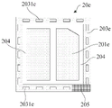
203e 隔离带203e Barrier
2031e 镂空图案2031e Cutout Pattern
20f 金属凸台20f metal boss
201f 固晶区201f Die bonding area
202f-P 正电极区202f-P positive electrode region
202f-N 负电极区202f-N Negative Electrode Region
203f 隔离带203f barrier tape
2031f 镂空图案2031f Cutout Pattern
205f 保护器件封装区205f protects the device package area
20g 金属凸台20g metal boss
201g 固晶区201g die bonding area
202g-P 正电极区202g-P positive electrode area
202g-N 负电极区202g-N Negative Electrode Region
203g 隔离带203g isolation tape
2031g 镂空图案2031g cutout pattern
205g 保护器件封装区205g protects the device package area
30 倒装LED芯片30 Flip-chip LED chips
30f 垂直LED芯片30f vertical LED chip
40 封装胶体40 Encapsulant
50 焊盘50 pads
60 导电部60 Conductive part
F 切割方向F Cutting direction
具体实施方式Detailed ways
以下通过特定的具体实例说明本发明的实施方式,本领域技术人员可由本说明书所揭露的内容轻易地了解本发明的其他优点与功效。本发明还可以通过另外不同的具体实施方式加以实施或应用,本说明书中的各项细节也可以基于不同观点与应用,在没有背离本发明的精神下进行各种修饰或改变。The embodiments of the present invention are described below through specific specific examples, and those skilled in the art can easily understand other advantages and effects of the present invention from the contents disclosed in this specification. The present invention can also be implemented or applied through other different specific embodiments, and various details in this specification can also be modified or changed based on different viewpoints and applications without departing from the spirit of the present invention.
无机氟树脂材料的折射率n约为1.34,紫外光透射率高,可靠性好,因此该氟树脂材料是非常好的深紫外LED封装材料。但是,含氟材料因为粘附性问题,特别难加工,容易出现切割脱落,震动脱落,回流焊气泡等问题。The refractive index n of the inorganic fluororesin material is about 1.34, the ultraviolet light transmittance is high, and the reliability is good, so the fluororesin material is a very good deep ultraviolet LED packaging material. However, fluorine-containing materials are particularly difficult to process due to the problem of adhesion, and are prone to problems such as cutting off, vibration falling off, and reflow soldering bubbles.
实施例一Example 1
本实施例提供一种LED封装器件制造方法,如图1-图4所示,包括如下步骤:This embodiment provides a method for manufacturing an LED package device, as shown in FIG. 1 to FIG. 4 , including the following steps:
提供一基板10,基板10包括上表面和下表面,所述基板10可以选择本领域常用的材料制成,例如陶瓷或硅,优选地为陶瓷基板。A
如图2所示,在基板10的上表面形成至少一个金属凸台20,如图2所示,金属凸台20之间具有第一间隔101,即金属凸台以第一间距L1间隔排列。As shown in FIG. 2 , at least one
接下来,如图3所示,将LED芯片30设置在金属凸台20上,本实施例中,LED芯片是倒装LED芯片。Next, as shown in FIG. 3 , the
参照附图6,示出了图3中圆圈部分的结构沿A-A方向的示意图。由图6可以看出,金属凸台20包括中间部分的用于设置倒装LED芯片30的固晶区201,固晶区201包括相对设置的正极固晶区2011和负极固晶区2012(正极固晶区2011和负极固晶区2012的位置不一定是图中所示右侧为正极固晶区2011、左侧为负极固晶区2012,固晶区的极性是由倒装设置在其上的LED芯片的正负极决定,此处仅为了便于说明定义图中的正极固晶区和负极固晶区的位置),LED芯片是倒装的,其正极和负极分别与正极固晶区2011和负极固晶区2012连接。如图6所示,正极固晶区2011和负极固晶区2012之间具有第二间隔102,即正极固晶区2011和负极固晶区2012之间具有第二间距为L2。该第二间距L2以及图2所示的金属凸台20之间的第一间距L1可以根据LED芯片的实际大小以及所要形成的封装器件的尺寸要求来确定。Referring to FIG. 6 , a schematic diagram of the structure of the circled portion in FIG. 3 along the AA direction is shown. As can be seen from FIG. 6 , the
仍然参照图6,金属凸台20的边缘部分形成隔离带203,隔离带203与固晶区201之间存在凹陷区204,凹陷区的厚度小于隔离带203的厚度和/或凹陷区的厚度小于固晶区201的厚度,隔离带203和固晶区201的厚度相等。优选地,所述凹陷区204的高度/宽度比例大于或等于1/2,其中所述凹陷区204的高度等于所述金属凸台的高度。Still referring to FIG. 6 , the edge portion of the
如图6所示,本实施例中隔离带203大体上可以看做是相互分离的两部分结构,这两部分结构均具有类似L型的结构,并且隔离带203的其中一部分与正极固晶区2011形成连续结构,另一部分与负极固晶区2012形成连续结构。由于正极固晶区2011和负极固晶区2012分别与LED芯片的正极和负极连通,而隔离带的两部分分别于正极固晶区2011和负极固晶区2012形成连续的结构,因此隔离带203可以作为LED芯片的电极区,并且与正极固晶区2011连续的隔离带部分形成LED芯片的正电极区,与负极固晶区2012连续的隔离带部分形成LED芯片的负电极区。As shown in FIG. 6 , in this embodiment, the
在本实施例的优选实施例中,可以首先通过离子溅射工艺在基板10上形成一金属薄层,然后再通过电镀或者化学镀工艺形成本实施例所述的金属凸台20。具体地可以包括以下步骤:In a preferred embodiment of this embodiment, a thin metal layer may be formed on the
首先,制作具有所述图案结构的掩膜版,并将该掩膜版贴附在基板10的上表面;例如可以采用胶粘剂等将掩膜版贴附在基板10的上表面。First, a mask with the pattern structure is fabricated, and the mask is attached to the upper surface of the
贴附了所述掩膜版之后,通过掩膜版对基板10的上表面进行镀金属层处理,例如通过离子溅射工艺在基板10的上表面形成具有所述图案结构的金属膜;该金属膜为基板10上的一层很薄的金属层,比如10~200μm。After the mask is attached, the upper surface of the
继续对所述金属膜进行镀金属层使所述金属膜厚度增加,例如通过电镀工艺或化学镀工艺对金属膜进行进一步镀金属层,使其厚度增加,直至形成所述金属凸台。Continuing to perform metal plating on the metal film increases the thickness of the metal film. For example, the metal film is further plated with a metal layer through an electroplating process or an electroless plating process to increase the thickness until the metal bosses are formed.
同样参照附图6,在本实施例的一优选实施例中,金属凸台20的隔离带203的一侧形成有静电保护器件(Zener)封装区205,在该保护器件封装区205中封装保护器件,对整个LED封装器件起到保护作用,例如该静电器件封装区205可以形成在隔离带的一侧边角位置。Referring also to FIG. 6 , in a preferred embodiment of this embodiment, an electrostatic protection device (Zener)
然后,如图4所示,将封装胶体40覆盖在LED芯片30、金属凸台20及基板10上,在本实施例的优选实施例中,封装胶体40优选氟树脂材料。对覆盖了上述封装胶体40的LED封装体进行加热,例如可以进行真空加压或者溶液烘烤或热压,使封装胶体40填充金属凸台20之间的第一间隔101及金属凸台内部固晶区201中的第二间隔102、隔离带和固晶区之间的凹陷区204以及隔离带203的两部分之间的缝隙等。经该加热过程后封装胶体与LED芯片30、金属凸台20以及基片之间形成良好的接触。然后对所述封装体进行冷却,封装胶体粘附在LED芯片30、金属凸台20及基板10上,并且封装胶体因填充了上述金属凸台凹陷区、缝隙等而与金属凸台20之间能够形成卡扣连接,该卡扣连接能够增加封装胶体的粘附力,有效防止封装体在运输或传送过程中出现封装胶体震动脱落等问题。Then, as shown in FIG. 4 , the
另外,因为陶瓷的膨胀系数为1.8*10-5/℃,氟树脂材料的热膨胀系数一般为8~12*10-5/℃,二者的膨胀系数相差较大,在封装器件经历上述的加热及冷却的较大的温度变化时,封装胶体40和金属凸台20之间的卡扣连接能够有效减少金属凸台20外的封装胶体40的形变,从而避免封装胶体40和基板10之间出现缝隙。In addition, because the expansion coefficient of ceramics is 1.8*10 -5 /°C, and the thermal expansion coefficient of fluororesin materials is generally 8~12*10 -5 /°C, the expansion coefficients of the two are quite different. When there is a large temperature change during cooling and cooling, the snap connection between the encapsulant 40 and the
在本实施例的优选实施例中,形成在基板10上的至少一个金属凸台20具有相同的厚度,并且金属凸台20(即其中的隔离带203和固晶区201)的厚度大于等于封装胶体40厚度的0.1倍,金属凸台20和封装胶体40边缘厚度小于等于0.1mm,金属凸台20的边缘距封装胶体40边缘的距离小于等于0.1mm,金属凸台20的宽度大于等于封装胶体厚度的1/3,所述金属凸台20的宽度指所述金属凸台20在垂直于切割方向(参照附图4所示的切割方向F)上的宽度。In a preferred embodiment of this embodiment, at least one
在本实施例的另一优选实施例中,如图5所示,还包括在基板10中形成导电部60,该导电部60包括分别与LED芯片30的正极和负极导通的正极导电部和负极导电部。导电部60包括贯穿所述基本10的导电孔等类似结构。In another preferred embodiment of this embodiment, as shown in FIG. 5 , a
然后在基板10的下表面形成焊盘50,焊盘50包括分别与上述导电部60的正极导电部和负极导电部导通的正极焊盘以及负极焊盘。例如,在图6所示的结构中,导电部60通过隔离带203实现与LED芯片的正极和负极导通,焊盘50与导电部60导通,从而实现焊盘与LED芯片的正极和负极连通。Then, a
如上所述在基板10的下表面形成焊盘50便于后续将LED封装器件形成后续的表面贴装器件。并且例如在采用回流焊技术将上述LED封装器件焊接到PCB(电路印刷板)板材上时,封装胶体40和金属凸台20之间形成的卡扣连接使得封装胶体与基板、金属凸台和LED芯片之间的紧密粘结,在上述回流焊过程中,不会产生气泡等缺陷,因此相应地能够提高后期产品的良率。Forming the
实施例二Embodiment 2
本实施例同样提供一种LED封装器件制造方法,与实施例一的相同之处不再赘述,不同之处在于:This embodiment also provides a method for manufacturing an LED package device, and the same points as those in the first embodiment will not be repeated, but the differences are:
本实施例中,形成金属凸台20a时,在金属凸台20a的隔离带203a中形成有各种图案结构。如图7所示,在隔离带203a中形成锯齿状的图案2031a。该锯齿状图案2031a可以是向内的锯齿,也可以是向外的锯齿。In this embodiment, when forming the
形成上述锯齿状图案之后,封装胶体填充在锯齿状图案形成的缝隙中,由此增强了封装胶体与金属凸台20a之间的卡扣连接,增强封装胶体与金属凸台20a、基板10的粘结。After the above-mentioned zigzag pattern is formed, the encapsulant is filled in the gap formed by the zigzag pattern, thereby enhancing the snap connection between the encapsulant and the
在本实施例的一优选实施例中,如图8所示,在隔离带203b中形成镂空图案2031b。该镂空图案2031b可以是矩形的镂空图案,也可以是菱形、椭圆形、圆形等镂空图案。In a preferred embodiment of this embodiment, as shown in FIG. 8 , a
在本实施例的另一优选实施例中,如图9所示,在形成金属凸台20c时,为了防止隔离带203c形成的L型区域过大,在L型区域的一侧形成镂空图案,例如形成圆形和/或矩形镂空图案2031c。In another preferred embodiment of this embodiment, as shown in FIG. 9 , when forming the
形成上述镂空图案之后,封装胶体填充在镂空图案形成的孔洞中,由此增强了封装胶体与金属凸台20b(或20c)之间的卡扣连接,增强封装胶体与金属凸台20b(或20c)、基板10的粘结。After the hollow pattern is formed, the encapsulating compound is filled in the holes formed by the hollow pattern, thereby enhancing the snap connection between the encapsulating compound and the
实施例三Embodiment 3
本实施例同样提供一种LED封装器件制造方法,与实施例二的相同之处不再赘述,不同之处在于:This embodiment also provides a method for manufacturing an LED package device, and the same points as those in the second embodiment will not be repeated, but the differences are:
如图10所示,本实施例中,形成金属凸台20d时,固晶区201d与隔离带203d同样形成连续结构,并且二者之间不存在凹陷区。固晶区201d和隔离带203d整体上形成互相隔离的两部分,这两部分分别包括正极固晶区2011d和负极固晶区2012d,并且与正极固晶区2011d连续的隔离带203d的部分可以作为LED芯片的正电极区,与负极固晶区2012d连续的隔离带203d的部分可以作为LED芯片的负电极区。As shown in FIG. 10 , in this embodiment, when the
在本实施例中,金属凸台20d的隔离带203d中同样形成有镂空图案,例如图10所示的矩形镂空图案2031d。当然,也可以包括例如菱形、圆形、椭圆形等其他图形的镂空图案。In this embodiment, a hollow pattern is also formed in the
封装胶体填充在上述镂空图案形成的孔洞中,由此增强了封装胶体与金属凸台20d之间的卡扣连接,增强封装胶体与金属凸台20d、基板10的粘结。The encapsulant is filled in the holes formed by the hollow pattern, thereby enhancing the snap connection between the encapsulant and the
实施例四Embodiment 4
本实施例同样提供一种LED封装器件制造方法,与实施例一的相同之处不再赘述,不同之处在于:This embodiment also provides a method for manufacturing an LED package device, and the same points as those in the first embodiment will not be repeated, but the differences are:
如图11所示,金属凸台20e同样包括固晶区201e和隔离带203e,本实施例中,隔离带203e形成封闭的结构,并且与固晶区201e相互隔离,二者之间具有凹陷区204并且由凹陷区204进行隔离。隔离带203e中可以形成图案结构,例如图11所示的矩形镂空图案2031e,当然也可以形成其他形状(例如菱形、椭圆形、圆形等)的镂空图案。并且也可以形成与图7所示的类似的锯齿状图案等。As shown in FIG. 11 , the
本实施例中,由于固晶区201e和隔离带203e是相互分离的结构,二者在结构上不连续,因此二者也不能形成电导通结构,因此,在本实施例中,与LED芯片的正极连接的正极固晶区形成LED芯片的正极电极区,与LED芯片的负极连接的负极固晶区形成LED芯片的负极电极区。In this embodiment, since the die-
在本实施例所述的封装器件制造方法中,形成的导电部通过固晶区201e与LED芯片的正极和负极连通,焊盘与导电部连通,从而实现与LED芯片的正极和负极连通。In the packaging device manufacturing method described in this embodiment, the formed conductive portion is connected to the positive and negative electrodes of the LED chip through the die-
实施例五Embodiment 5
如图12所示,本实施例同样提供一种LED封装器件制造方法,同样包括如下步骤:As shown in FIG. 12 , this embodiment also provides a method for manufacturing an LED package device, which also includes the following steps:
提供基板10,基板10包括上表面和下表面,所述基板10可以选择本领域常用的材料制成,例如陶瓷或硅,优选地为陶瓷基板。A
在基板10的上表面形成至少一个金属凸台20f。At least one
将LED芯片30f设置在金属凸台20f上。The
本实施例与上述实施例一到实施例四的相同之处不再赘述,不同之处在于:The similarities between this embodiment and the above-mentioned Embodiments 1 to 4 will not be repeated, and the differences are:
在本实施例中,LED芯片30f优选地是垂直LED芯片,在本实施例中,形成金属凸台20f时,固晶区201f与隔离带203f形成相互分隔的结构,二者之间具有凹陷区204并且由凹陷区204相互隔离。并且隔离带203f中形成有镂空图案,例如图12所示的矩形镂空图案2031f。当然也可以包括其他图形(例如圆形、菱形、椭圆形等)的镂空图案。In this embodiment, the
如图12所示,固晶区201f同样包括正极固晶区2011f和负极固晶区2012f,本实施例的垂直LED芯片30f设置在正极固晶区2011f中,并且正极固晶区的2011f一侧的部分区域包括延伸部分,优选地,该延伸部分自正极固晶区2011f一侧小于固晶区宽度的1/2的区域延伸,例如图12所示的自正极固晶区2011f下方一侧的左边小于正极固晶区2011f宽度的1/2的区域延伸。该延伸部分形成与LED芯片的正极接触的正电极区202f-P。如图12所示,负极固晶区2012f形成在正电极区202f-P的同一侧与正电极区202f-P相邻,并且该负极固晶区2012f与隔离带203f及正电极区202f-P均相互间隔,形成独立的结构。在LED芯片30f的负极表面与负极固晶区2012f之间形成使二者电导通的负极焊线206f,此时,负极固晶区2012f形成LED芯片30f的负电极区202f-N。金属凸台20f还包括在该正电极区202f-P和负电极区202f-N中形成的保护器件封装区205f。As shown in FIG. 12 , the
如图12所示,优选地,该正电极区202f-P、负电极区202f-N及二者之间的间隔的总宽度不超过正极固晶区2011f设置LED芯片的区域的宽度。As shown in FIG. 12 , preferably, the total width of the
如图13所示,在本实施例的一优选实施例中,形成金属凸台20g时,不单独形成图12所示的负电极区202f-N,而是在LED芯片30f的负极表面和隔离带203g之间形成使二者电导通的负极焊线206g,此时,隔离带203g同时作为LED芯片30f的负电极区202g-N。并且在正电极区202g-P和隔离带203g中形成保护器件封装区205g。并且隔离带203g中同样形成有镂空图案2031g,例如图13所示的矩形镂空图案2031g。当然也可以包括其他图形(例如圆形、菱形、椭圆形等)的镂空图案。As shown in FIG. 13 , in a preferred embodiment of this embodiment, when forming the
封装胶体填充在上述镂空图案形成的孔洞中,由此增强了封装胶体与金属凸台20f(或20g)之间的卡扣连接,增强封装胶体与金属凸台20f(或20g)、基板10的粘结。The encapsulant is filled in the holes formed by the hollow pattern, thereby enhancing the snap connection between the encapsulant and the
实施例六Embodiment 6
本实施例同样提供一种LED封装器件制造方法,与上述实施例一至实施例五的相同之处不再赘述,不同之处在于:This embodiment also provides a method for manufacturing an LED package device, and the same points as the above-mentioned Embodiments 1 to 5 will not be repeated, and the differences are:
本实施例的制造方法还包括对所述封装器件进行切割。包括沿图2所示的所述第一间隔101的中间位置,沿图4所示的切割方向F以单个发光体为单元对所述封装器件进行切割,得到图14所示的单个发光体器件。The manufacturing method of this embodiment further includes cutting the packaged device. The encapsulated device is cut along the middle position of the
由于封装胶体40和金属凸台20之间形成了上述的卡扣连接,因此在切割时,上述卡扣连接能够起到阻挡的作用,有效减少封装胶体底部的形变量,保证靠近金属凸台的固晶区的封装胶体和基板紧密结合,不会因为切割受力而从基板剥离。Since the above-mentioned snap connection is formed between the encapsulating
实施例七Embodiment 7
本实施例提供一种LED封装器件,再次参照图4和图5,该LED封装器件包括:This embodiment provides an LED package device. Referring to FIG. 4 and FIG. 5 again, the LED package device includes:
基板10,包括上表面和下表面,所述基板10可以选择本领域常用的材料制成,例如陶瓷或硅,优选地为陶瓷基板。The
设置在所述基板10的上表面上的至少一个金属凸台20,例如,金属凸台20可以是通过溅射工艺结合电镀或者化学镀工艺在陶瓷基板上形成的金属镀层,该金属镀层可以是铜镀层。如图2所示,金属凸台20之间具有第一间隔101,即金属凸台以第一间距L1间隔排列。At least one
设置在所述金属凸台20上的LED芯片30,本实施例中,LED芯片是倒装的LED芯片。The LED chips 30 disposed on the
参照附图6,示出了图3中圆圈部分的结构沿A-A方向的示意图。由图6可以看出,金属凸台20包括中间部分的用于设置LED芯片30的固晶区201,固晶区201包括相对设置的正极固晶区2011和负极固晶区2012(正极固晶区2011和负极固晶区2012的位置不一定是图中所示右侧为正极固晶区2011、左侧为负极固晶区2012,固晶区的极性是由倒装设置在其上的LED芯片的正负极决定,此处仅为了便于说明定义图中的正极固晶区和负极固晶区的位置),LED芯片是倒装的,其正极和负极分别与正极固晶区2011和负极固晶区2012连接。如图6所示,正极固晶区2011和负极固晶区2012之间具有第二间隔102,即正极固晶区2011和负极固晶区2012之间具有第二间距为L2。该第二间距L2以及图2所示的金属凸台20之间的第一间距L1可以根据LED芯片的实际大小以及所要形成的封装器件的尺寸要求来确定。Referring to FIG. 6 , a schematic diagram of the structure of the circled portion in FIG. 3 along the AA direction is shown. As can be seen from FIG. 6 , the
仍然参照图6,金属凸台20的边缘部分形成隔离带203,隔离带203与固晶区201之间存在凹陷区204,凹陷区的厚度小于隔离带203的厚度以及固晶区201的厚度,隔离带203和固晶区201的厚度相等。优选地,所述凹陷区204的高度/宽度大于或等于1/2,其中所述凹陷区204的高度等于所述金属凸台的高度。Still referring to FIG. 6 , the edge portion of the
如图6所示,本实施例中隔离带203大体上可以看做是相互分离的两部分结构,这两部分结构均具有类似L型的结构,并且隔离带203的其中一部分与正极固晶区2011形成连续结构,另一部分与负极固晶区2012形成连续结构。由于正极固晶区2011和负极固晶区2012分别与LED芯片的正极和负极连通,而隔离带的两部分分别于正极固晶区2011和负极固晶区2012形成连续的结构,因此隔离带203可以作为LED芯片的电极区202,并且与正极固晶区2011连续的隔离带部分形成LED芯片的正电极区,与负极固晶区2012连续的隔离带部分形成LED芯片的负电极区。As shown in FIG. 6 , in this embodiment, the
在本实施例中,可以首先通过离子溅射工艺在基板10上形成一金属薄层,然后再通过电镀或者化学镀工艺形成本实施例所述的金属凸台20。In this embodiment, a thin metal layer may be formed on the
同样参照附图6,在本实施例的一优选实施例中,金属凸台20的隔离带203的一侧形成有静电保护器件(Zener)封装区205,在该保护器件封装区205中封装保护器件,对整个LED封装器件起到保护作用,例如该静电器件封装区205可以形成在隔离带的一侧边角位置。Referring also to FIG. 6 , in a preferred embodiment of this embodiment, an electrostatic protection device (Zener)
然后,如图4所示,将封装胶体40覆盖在LED芯片30、金属凸台20及基板10上,在本实施例的优选实施例中,封装胶体40优选氟树脂材料。对覆盖了上述封装胶体40的LED封装体进行加热,例如可以进行溶液烘烤或热压,使封装胶体40填充金属凸台20之间的第一间隔101及金属凸台内部固晶区201中的第二间隔102、隔离带和固晶区之间的凹陷区204以及隔离带203的两部分之间的缝隙等。经该加热过程后封装胶体与LED芯片30、金属凸台20以及基片之间形成良好的接触。然后对所述封装体进行冷却,封装胶体粘附在LED芯片30、金属凸台20及基板10上,并且封装胶体因填充了上述金属凸台凹陷区、缝隙等而与金属凸台20之间能够形成卡扣连接,该卡扣连接能够增加封装胶体的粘附力,有效防止封装体在运输或传送过程中出现封装胶体震动脱落等问题。Then, as shown in FIG. 4 , the
另外,因为陶瓷的膨胀系数为1.8*10-5/℃,氟树脂材料的热膨胀系数一般为8-12*10-5/℃,二者的膨胀系数相差较大,在封装器件经历上述的加热及冷却的较大的温度变化时,封装胶体40和金属凸台20之间的卡扣连接能够有效减少金属凸台20外的封装胶体40的形变,从而避免封装胶体40和基板10之间出现缝隙。In addition, because the expansion coefficient of ceramics is 1.8*10 -5 /°C, and the thermal expansion coefficient of fluororesin materials is generally 8-12*10 -5 /°C, the expansion coefficients of the two are quite different. When there is a large temperature change during cooling and cooling, the snap connection between the encapsulant 40 and the
在本实施例的优选实施例中,金属凸台20具有相同的厚度,并且金属凸台20的厚度大于等于封装胶体40厚度的0.1倍,金属凸台20和封装胶体40边缘厚度小于等于0.1mm,金属凸台20的边缘距封装胶体40边缘的距离小于等于0.1mm,金属凸台20的宽度大于等于封装胶体厚度的1/3,所述金属凸台20的宽度指所述金属凸台20在垂直于切割方向(参照附图4所示的切割方向F)上的宽度。In a preferred embodiment of this embodiment, the
在本实施例的另一优选实施例中,如图5所示,LED封装器件的基板10还包括导电部60,该导电部60包括分别与正电极区和负电极区对应的正极导电部和负极导电部。导电部60包括贯穿所述基本10的导电孔等类似结构。In another preferred embodiment of this embodiment, as shown in FIG. 5 , the
以及形成在基板10的下表面的焊盘50,焊盘50包括分别与上述导电部60的正极导电部和负极导电部导通的正极焊盘以及负极焊盘。例如,在图6所示的结构中,导电部60通过隔离带203实现与LED芯片的正极和负极导通,焊盘50与导电部60导通,从而实现焊盘与LED芯片的正极和负极连通。and a
如上所述在基板10的下表面形成的焊盘50便于后续将LED封装器件形成后续的表面贴装器件。并且例如在采用回流焊技术将上述LED封装器件焊接到PCB(电路印刷板)板材上时,封装胶体40和金属凸台20之间形成的卡扣连接使得封装胶体与基板、金属凸台和LED芯片之间的紧密粘结,在上述回流焊过程中,不会产生气泡等缺陷,因此相应地能够提高后期产品的良率。The
实施例八Embodiment 8
本实施例提供一种LED封装器件,与实施例五的相同之处不再赘述,不同之处在于:This embodiment provides an LED package device, and the similarities with Embodiment 5 will not be repeated, but the differences are:
本实施例中,金属凸台20a的隔离带203a中具有各种图案结构。如图7所示,隔离带203a中包括锯齿状的图案2031a。该锯齿状图案2031a可以是向内的锯齿,也可以是向外的锯齿。In this embodiment, the isolation strips 203a of the
形成上述锯齿状图案之后,封装胶体填充在锯齿状图案形成的缝隙中,由此增强了封装胶体与金属凸台20a之间的卡扣连接,增强封装胶体与金属凸台20a、基板10的粘结。After the above-mentioned zigzag pattern is formed, the encapsulant is filled in the gap formed by the zigzag pattern, thereby enhancing the snap connection between the encapsulant and the
在本实施例的一优选实施例中,如图8所示,隔离带203b中包括镂空图案2031b。该镂空图案2031b可以是矩形的镂空图案,也可以是菱形、椭圆形、圆形等镂空图案。In a preferred embodiment of this embodiment, as shown in FIG. 8 , the
在本实施例中,如图9所示,为了防止金属凸台20c的隔离带203c的L型区域过大,在L型区域的一侧包括镂空图案,例如包括圆形和/或矩形镂空图案2031c。In this embodiment, as shown in FIG. 9 , in order to prevent the L-shaped area of the
形成上述镂空图案之后,封装胶体填充在镂空图案形成的孔洞中,由此增强了封装胶体与金属凸台20b之间的卡扣连接,增强封装胶体与金属凸台20b、基板10的粘结。After the hollow pattern is formed, the encapsulant is filled in the holes formed by the hollow pattern, thereby enhancing the snap connection between the encapsulant and the
实施例九Embodiment 9
如图10所示,本实施例中,金属凸台20d的固晶区201d与隔离带203d同样包括连续结构,并且二者之间不存在凹陷区。固晶区201d和隔离带203d整体上形成互相隔离的两部分,这两部分分别包括正极固晶区2011d和负极固晶区2012d,并且与正极固晶区2011d连续的隔离带203d的部分可以作为LED芯片的正电极区,与负极固晶区2012d连续的隔离带203d的部分可以作为LED芯片的负电极区。As shown in FIG. 10 , in this embodiment, the die-
在本实施例中,金属凸台20d的隔离带203d中同样形成有镂空图案,例如图10所示的矩形镂空图案2031d。当然,也可以包括例如菱形、圆形、椭圆形等其他图形的镂空图案。In this embodiment, a hollow pattern is also formed in the
封装胶体填充在上述镂空图案形成的孔洞中,由此增强了封装胶体与金属凸台20d之间的卡扣连接,增强封装胶体与金属凸台20d、基板10的粘结。The encapsulant is filled in the holes formed by the hollow pattern, thereby enhancing the snap connection between the encapsulant and the
实施例十Embodiment ten
本实施例同样提供一种LED封装器件,与实施例五的相同之处不再赘述,不同之处在于:This embodiment also provides an LED package device, and the similarities with the fifth embodiment will not be repeated, but the differences are:
如图11所示,金属凸台20e同样包括固晶区201e和隔离带203e,本实施例中,隔离带203e为封闭的结构,并且与固晶区201e相互隔离,二者之间由凹陷区204进行隔离。隔离带203e中可以包括图案结构,例如图11所示的矩形镂空图案2031e,当然也可以包括其他形状(例如菱形、椭圆形、圆形等)的镂空图案。并且也可以包括与图7所示的类似的锯齿状图案等。As shown in FIG. 11 , the
本实施例中,由于固晶区201e和隔离带203e是相互分离的结构,二者在结构上不连续,因此二者也不能形成导通结构,因此,在本实施例中,与LED芯片的正极连接的正极固晶区形成LED芯片的正极电极区,与LED芯片的负极连接的负极固晶区形成LED芯片的负极电极区。In this embodiment, since the die-
在本实施例所述的封装器件中,导电部通过固晶区201e与LED芯片的正极和负极连通,焊盘与导电部连通,从而实现与LED芯片的正极和负极连通。In the packaged device described in this embodiment, the conductive portion communicates with the positive electrode and the negative electrode of the LED chip through the die-
实施例十一Embodiment 11
本实施例同样提供一种LED封装器件,同样包括:This embodiment also provides an LED package device, which also includes:
如图12所示,提供基板10,基板10包括上表面和下表面,所述基板10可以选择本领域常用的材料制成,例如陶瓷或硅,优选地为陶瓷基板。As shown in FIG. 12 , a
形成在基板10的上表面的至少一个金属凸台20f。At least one
设置在金属凸台20f上的LED芯片30f。The
本实施例与上述实施例七到实施例十的相同之处不再赘述,不同之处在于:The similarities between this embodiment and the above-mentioned Embodiment 7 to
在本实施例中,LED芯片30f优选地是垂直LED芯片,在本实施例中,金属凸台20f的固晶区201f与隔离带203f形成相互分隔的结构,二者之间具有凹陷区204并且由凹陷区204相互隔离。并且隔离带203f包括镂空图案,例如图12所示的矩形镂空图案2031f。当然也可以包括其他图形(例如圆形、菱形、椭圆形等)的镂空图案。In this embodiment, the
如图12所示,固晶区201f同样包括正极固晶区2011f和负极固晶区2012f,本实施例的垂直LED芯片30f设置在正极固晶区2011f中,并且正极固晶区2011f的一侧的一部分区域包括延伸部分,优选地,该延伸部分自正极固晶区2011f一侧小于固晶区宽度的1/2的区域延伸,例如图12所示的自正极固晶区2011f下方一侧的左边小于正极固晶区2011f宽度的1/2的区域向下延伸。该延伸部分形成与LED芯片的正极接触的正电极区202f-P。如图12所示,负极固晶区2012f形成在正电极区202f-P的同一侧与正电极区202f-P相邻,并且该负极固晶区2012f与隔离带203f及正电极区202f-P均相互间隔,形成独立的结构。在LED芯片30f的负极表面与负极固晶区2012f之间形成使二者电导通的负极焊线206f,此时,负极固晶区2012f形成LED芯片30f的负电极区202f-N。金属凸台20f还包括在该正电极区202f-P和负电极区202f-N中形成的保护器件封装区205f。As shown in FIG. 12 , the
如图12所示,优选地,该正电极区202f-P、负电极区202f-N及二者之间的间隔的总宽度不超过正极固晶区2011f设置LED芯片的区域的宽度。As shown in FIG. 12 , preferably, the total width of the
如图13所示,在本实施例的一优选实施例中,形成金属凸台20g时,不单独形成图12所示的负电极区202f-N,而是在LED芯片30f的负极表面和隔离带203g之间形成使二者电导通的负极焊线206g,此时,隔离带203g同时作为LED芯片30f的负电极区202g-N。并且在正电极区202g-P和隔离带203g中形成保护器件封装区205g。并且隔离带203g中同样形成有镂空图案2031g,例如图13所示的矩形镂空图案2031g。当然也可以包括其他图形(例如圆形、菱形、椭圆形等)的镂空图案。As shown in FIG. 13 , in a preferred embodiment of this embodiment, when forming the
封装胶体填充在上述镂空图案形成的孔洞中,由此增强了封装胶体与金属凸台20f(或20g)之间的卡扣连接,增强封装胶体与金属凸台20f(或20g)、基板10的粘结。The encapsulant is filled in the holes formed by the hollow pattern, thereby enhancing the snap connection between the encapsulant and the
实施例十二Embodiment 12
本实施例同样提供一种LED封装器件,与实施例十一的相同之处不再赘述,不同之处在于:This embodiment also provides an LED package device, and the similarities with the eleventh embodiment will not be repeated, but the differences are:
本实施例的封装器件包括图14所示的单个发光体器件,该单个发光器件包括沿图2所示的第一间隔101的中间位置,沿图4所示的切割方向F自封装器件中切割出的单个发光体。由于封装胶体40和金属凸台20之间形成了卡扣连接,因此该封装器件在使用过程中不易出现封装胶体脱落或剥离等问题。The packaged device of this embodiment includes a single light-emitting body device shown in FIG. 14 , and the single light-emitting device includes a middle position along the
如上所述,本发明的LED封装器件及其制造方法,至少包括以下有益效果:As mentioned above, the LED package device and the manufacturing method thereof of the present invention at least include the following beneficial effects:
本发明的方法在金属凸台中形成图案,封装胶体不仅覆盖LED芯片、金属凸台和基板,同时还填充金属凸台之间的间隙以及金属凸台中的图案形成的空隙或孔洞,由此,封装胶体和金属凸台之间形成卡扣连接。增加了封装胶体的粘附力,有效防止封装体在运输或传送过程中出现封装胶体震动脱落等问题。The method of the present invention forms patterns in the metal bosses, and the encapsulation colloid not only covers the LED chip, the metal bosses and the substrate, but also fills the gaps between the metal bosses and the gaps or holes formed by the patterns in the metal bosses. A snap connection is formed between the colloid and the metal boss. The adhesive force of the encapsulation colloid is increased, which effectively prevents the encapsulation colloid from vibrating and falling off during transportation or transmission.
由于封装胶体和LED芯片、金属凸台及基板间的紧密粘结,有效避免例如通过回流焊在基板的下表面形成焊盘时,出现回流焊气泡等缺陷,从而保证后续产品的良率。Due to the close bonding between the encapsulation colloid, the LED chip, the metal boss and the substrate, defects such as reflow soldering bubbles are effectively avoided when forming pads on the lower surface of the substrate by reflow soldering, thereby ensuring the yield of subsequent products.
在切割时,封装胶体和金属凸台之间的上述卡扣连接能够起到阻挡的作用,有效减少封装胶体底部的形变量,保证靠近金属凸台的固晶区的封装胶体和基板紧密结合,不会因为切割受力而从基板剥离。During cutting, the above-mentioned snap connection between the encapsulation colloid and the metal boss can play a blocking role, effectively reducing the deformation amount at the bottom of the encapsulating colloid, and ensuring that the encapsulating colloid and the substrate in the die-bonding area close to the metal boss are closely combined. Will not peel off from the substrate due to cutting force.
在封装体经历较大的温度变化时,尽管本发明中采用的陶瓷基板和氟树脂材料封装胶体的热膨胀系数相差较大,但是由于封装胶体和金属凸台之间能够形成卡扣连接,因此能够有效减少金属凸台外的封装胶体的形变,从而避免封装胶体和基板之间出现缝隙。When the package body undergoes a large temperature change, although the thermal expansion coefficients of the ceramic substrate and the fluororesin material encapsulant used in the present invention are quite different, since a snap connection can be formed between the encapsulant and the metal boss, it is possible to Effectively reduce the deformation of the encapsulation compound outside the metal boss, thereby avoiding a gap between the encapsulation compound and the substrate.
另外,本发明所述的LED封装器件的制备方法过程比较简单,封装效果好,有利于降低封装成本、增加经济效益。In addition, the preparation method of the LED packaging device of the present invention is relatively simple, and has good packaging effect, which is beneficial to reduce packaging costs and increase economic benefits.
上述实施例仅例示性说明本发明的原理及其功效,而非用于限制本发明。任何熟悉此技术的人士皆可在不违背本发明的精神及范畴下,对上述实施例进行修饰或改变。因此,举凡所属技术领域中具有通常知识者在未脱离本发明所揭示的精神与技术思想下所完成的一切等效修饰或改变,仍应由本发明的权利要求所涵盖。The above-mentioned embodiments merely illustrate the principles and effects of the present invention, but are not intended to limit the present invention. Anyone skilled in the art can modify or change the above embodiments without departing from the spirit and scope of the present invention. Therefore, all equivalent modifications or changes made by those with ordinary knowledge in the technical field without departing from the spirit and technical idea disclosed in the present invention should still be covered by the claims of the present invention.
Claims (12)
Priority Applications (1)
| Application Number | Priority Date | Filing Date | Title |
|---|---|---|---|
| CN202110323833.1A CN112864297B (en) | 2019-01-29 | 2019-01-29 | LED packaging device |
Applications Claiming Priority (2)
| Application Number | Priority Date | Filing Date | Title |
|---|---|---|---|
| CN201910086438.9A CN109830589B (en) | 2019-01-29 | 2019-01-29 | LED packaging device and manufacturing method thereof |
| CN202110323833.1A CN112864297B (en) | 2019-01-29 | 2019-01-29 | LED packaging device |
Related Parent Applications (1)
| Application Number | Title | Priority Date | Filing Date |
|---|---|---|---|
| CN201910086438.9A Division CN109830589B (en) | 2019-01-29 | 2019-01-29 | LED packaging device and manufacturing method thereof |
Publications (2)
| Publication Number | Publication Date |
|---|---|
| CN112864297A CN112864297A (en) | 2021-05-28 |
| CN112864297B true CN112864297B (en) | 2022-06-28 |
Family
ID=66862835
Family Applications (3)
| Application Number | Title | Priority Date | Filing Date |
|---|---|---|---|
| CN202110323833.1A Active CN112864297B (en) | 2019-01-29 | 2019-01-29 | LED packaging device |
| CN201910086438.9A Active CN109830589B (en) | 2019-01-29 | 2019-01-29 | LED packaging device and manufacturing method thereof |
| CN202110323687.2A Active CN112864296B (en) | 2019-01-29 | 2019-01-29 | An LED package device |
Family Applications After (2)
| Application Number | Title | Priority Date | Filing Date |
|---|---|---|---|
| CN201910086438.9A Active CN109830589B (en) | 2019-01-29 | 2019-01-29 | LED packaging device and manufacturing method thereof |
| CN202110323687.2A Active CN112864296B (en) | 2019-01-29 | 2019-01-29 | An LED package device |
Country Status (2)
| Country | Link |
|---|---|
| CN (3) | CN112864297B (en) |
| TW (1) | TWI740359B (en) |
Families Citing this family (9)
| Publication number | Priority date | Publication date | Assignee | Title |
|---|---|---|---|---|
| WO2021072663A1 (en) * | 2019-10-16 | 2021-04-22 | 泉州三安半导体科技有限公司 | Led packaging device and fabrication method therefor |
| CN111885826B (en) * | 2020-07-23 | 2022-07-26 | 东莞市豪顺精密科技有限公司 | Copper-clad layer structure of single-layer printed circuit board |
| JP6954701B1 (en) * | 2021-01-23 | 2021-10-27 | 三安ジャパンテクノロジー株式会社 | Elastic wave device |
| CN113299811A (en) * | 2021-05-06 | 2021-08-24 | 谢国州 | Novel COB anti-drop packaging method |
| CN113571476B (en) * | 2021-07-14 | 2024-11-05 | 上海富乐华半导体科技有限公司 | Chip packaging method |
| JP7361343B2 (en) * | 2021-09-29 | 2023-10-16 | 三安ジャパンテクノロジー株式会社 | module |
| CN113991004A (en) * | 2021-10-26 | 2022-01-28 | 东莞市中麒光电技术有限公司 | LED substrate manufacturing method, LED substrate, LED device manufacturing method and LED device |
| CN114267765B (en) * | 2021-12-06 | 2024-07-09 | 深圳市伟方成科技有限公司 | LED packaging device |
| TWI867530B (en) * | 2023-05-12 | 2024-12-21 | 友達光電股份有限公司 | Display panel |
Citations (5)
| Publication number | Priority date | Publication date | Assignee | Title |
|---|---|---|---|---|
| EP1244152A2 (en) * | 2001-01-26 | 2002-09-25 | Toyoda Gosei Co., Ltd. | Reflective light emitting diode, reflective optical device and its manufacturing method |
| CN101447541A (en) * | 2007-11-26 | 2009-06-03 | 斯坦雷电气株式会社 | Semiconductor device |
| CN102142513A (en) * | 2010-01-29 | 2011-08-03 | 株式会社东芝 | LED package and method for manufacturing same |
| CN102916112A (en) * | 2012-10-31 | 2013-02-06 | 佛山市国星光电股份有限公司 | Large power LED and manufacturing method thereof |
| CN106558640A (en) * | 2015-09-25 | 2017-04-05 | 光宝光电(常州)有限公司 | Package structure for LED and its manufacture method |
Family Cites Families (14)
| Publication number | Priority date | Publication date | Assignee | Title |
|---|---|---|---|---|
| US7534633B2 (en) * | 2004-07-02 | 2009-05-19 | Cree, Inc. | LED with substrate modifications for enhanced light extraction and method of making same |
| US7736945B2 (en) * | 2005-06-09 | 2010-06-15 | Philips Lumileds Lighting Company, Llc | LED assembly having maximum metal support for laser lift-off of growth substrate |
| US8877101B2 (en) * | 2007-05-31 | 2014-11-04 | Nthdegree Technologies Worldwide Inc | Method of manufacturing a light emitting, power generating or other electronic apparatus |
| TW200910639A (en) * | 2007-08-24 | 2009-03-01 | Hsin-Hui Yeh | LED package and method thereof |
| KR101192181B1 (en) * | 2010-03-31 | 2012-10-17 | (주)포인트엔지니어링 | Optical Element Device and Fabricating Method Thereof |
| WO2012057038A1 (en) * | 2010-10-26 | 2012-05-03 | 東芝ライテック株式会社 | Light-emitting module and lighting equipment |
| KR20130143061A (en) * | 2010-11-03 | 2013-12-30 | 쓰리엠 이노베이티브 프로퍼티즈 컴파니 | Flexible led device with wire bond free die |
| KR101761834B1 (en) * | 2011-01-28 | 2017-07-27 | 서울바이오시스 주식회사 | Wafer level led package and method of fabricating the same |
| JP2013033910A (en) * | 2011-06-29 | 2013-02-14 | Hitachi Cable Ltd | Substrate for mounting light emitting element, led package, and manufacturing method of led package |
| TW201312798A (en) * | 2011-09-02 | 2013-03-16 | Adl Engineering Inc | LED package structure having a light-reflecting cover and fabrication method thereof |
| JP5234219B1 (en) * | 2012-09-07 | 2013-07-10 | 三菱化学株式会社 | Light emitting diode element and light emitting device |
| KR102197082B1 (en) * | 2014-06-16 | 2020-12-31 | 엘지이노텍 주식회사 | Light emitting device and light emitting device package including the same |
| CN110235260A (en) * | 2017-01-31 | 2019-09-13 | 晶化成半导体公司 | For enhancing the method and encapsulation of the reliability of ultraviolet light emitting device |
| CN108231973B (en) * | 2017-12-08 | 2019-08-27 | 开发晶照明(厦门)有限公司 | Package Holder |
-
2019
- 2019-01-29 CN CN202110323833.1A patent/CN112864297B/en active Active
- 2019-01-29 CN CN201910086438.9A patent/CN109830589B/en active Active
- 2019-01-29 CN CN202110323687.2A patent/CN112864296B/en active Active
-
2020
- 2020-01-21 TW TW109102220A patent/TWI740359B/en active
Patent Citations (5)
| Publication number | Priority date | Publication date | Assignee | Title |
|---|---|---|---|---|
| EP1244152A2 (en) * | 2001-01-26 | 2002-09-25 | Toyoda Gosei Co., Ltd. | Reflective light emitting diode, reflective optical device and its manufacturing method |
| CN101447541A (en) * | 2007-11-26 | 2009-06-03 | 斯坦雷电气株式会社 | Semiconductor device |
| CN102142513A (en) * | 2010-01-29 | 2011-08-03 | 株式会社东芝 | LED package and method for manufacturing same |
| CN102916112A (en) * | 2012-10-31 | 2013-02-06 | 佛山市国星光电股份有限公司 | Large power LED and manufacturing method thereof |
| CN106558640A (en) * | 2015-09-25 | 2017-04-05 | 光宝光电(常州)有限公司 | Package structure for LED and its manufacture method |
Also Published As
| Publication number | Publication date |
|---|---|
| CN112864296B (en) | 2022-06-28 |
| TWI740359B (en) | 2021-09-21 |
| CN112864297A (en) | 2021-05-28 |
| CN109830589B (en) | 2021-04-16 |
| CN112864296A (en) | 2021-05-28 |
| TW202032819A (en) | 2020-09-01 |
| CN109830589A (en) | 2019-05-31 |
Similar Documents
| Publication | Publication Date | Title |
|---|---|---|
| CN112864297B (en) | LED packaging device | |
| CN102290524B (en) | LED (Light Emitting Diode) device and LED (Light Emitting Diode) module device thereof | |
| CN102916112B (en) | A kind of high power LED device and manufacture method thereof | |
| WO2012012975A1 (en) | Led chip surface mounted packaging structure based on silicon substrate and packaging method thereof | |
| US20130161670A1 (en) | Light emitting diode packages and methods of making | |
| US10461227B2 (en) | Method for manufacturing light emitting device, and light emitting device | |
| CN103199187B (en) | A kind of LED encapsulation substrate and encapsulating structure and preparation method thereof | |
| JP2007527123A (en) | Flip chip light emitting diode element without submount | |
| CN101567411A (en) | Flip-chip integrated encapsulation structure of LED and method thereof | |
| CN104022207B (en) | A kind of White-light LED chip and preparation method thereof | |
| CN106856220B (en) | Wafer-level packaged flip-chip LED device, dividing unit and manufacturing method thereof | |
| JP4590994B2 (en) | Light emitting device and manufacturing method thereof | |
| CN103236490B (en) | LED flip chip packaging, its manufacture method and use its encapsulating structure | |
| TW201342672A (en) | Method for manufacturing LED package | |
| CN107819065B (en) | Flip LED light-emitting device and preparation method thereof | |
| KR101426434B1 (en) | Manufacturing method of semiconductor light emitting device | |
| CN107123721A (en) | A kind of band lens type LED encapsulation structure and method for packing | |
| CN101442040B (en) | Light emitting diode packaging structure and manufacturing method thereof | |
| WO2022183393A1 (en) | Led packaging device and preparation method therefor | |
| CN202363515U (en) | LED device and LED module device thereof | |
| CN104638090B (en) | Flip LED encapsulation module | |
| US11398589B2 (en) | Light emitting device package and light source device | |
| TWI412163B (en) | Led package structure and the method of manufacturing the same | |
| WO2021072663A1 (en) | Led packaging device and fabrication method therefor | |
| CN105428505A (en) | Support used for LED flip die bond and die bond method utilizing support |
Legal Events
| Date | Code | Title | Description |
|---|---|---|---|
| PB01 | Publication | ||
| PB01 | Publication | ||
| SE01 | Entry into force of request for substantive examination | ||
| SE01 | Entry into force of request for substantive examination | ||
| GR01 | Patent grant | ||
| GR01 | Patent grant |