CN112563280A - Semiconductor device and method for manufacturing the same - Google Patents
Semiconductor device and method for manufacturing the same Download PDFInfo
- Publication number
- CN112563280A CN112563280A CN202010561455.6A CN202010561455A CN112563280A CN 112563280 A CN112563280 A CN 112563280A CN 202010561455 A CN202010561455 A CN 202010561455A CN 112563280 A CN112563280 A CN 112563280A
- Authority
- CN
- China
- Prior art keywords
- sub
- layer
- stop
- channel
- penetrating
- Prior art date
- Legal status (The legal status is an assumption and is not a legal conclusion. Google has not performed a legal analysis and makes no representation as to the accuracy of the status listed.)
- Granted
Links
Images


Classifications
-
- H—ELECTRICITY
- H10—SEMICONDUCTOR DEVICES; ELECTRIC SOLID-STATE DEVICES NOT OTHERWISE PROVIDED FOR
- H10B—ELECTRONIC MEMORY DEVICES
- H10B41/00—Electrically erasable-and-programmable ROM [EEPROM] devices comprising floating gates
- H10B41/20—Electrically erasable-and-programmable ROM [EEPROM] devices comprising floating gates characterised by three-dimensional [3D] arrangements, e.g. with cells on different height levels
- H10B41/23—Electrically erasable-and-programmable ROM [EEPROM] devices comprising floating gates characterised by three-dimensional [3D] arrangements, e.g. with cells on different height levels with source and drain on different levels, e.g. with sloping channels
- H10B41/27—Electrically erasable-and-programmable ROM [EEPROM] devices comprising floating gates characterised by three-dimensional [3D] arrangements, e.g. with cells on different height levels with source and drain on different levels, e.g. with sloping channels the channels comprising vertical portions, e.g. U-shaped channels
-
- H—ELECTRICITY
- H10—SEMICONDUCTOR DEVICES; ELECTRIC SOLID-STATE DEVICES NOT OTHERWISE PROVIDED FOR
- H10B—ELECTRONIC MEMORY DEVICES
- H10B43/00—EEPROM devices comprising charge-trapping gate insulators
- H10B43/10—EEPROM devices comprising charge-trapping gate insulators characterised by the top-view layout
-
- H—ELECTRICITY
- H10—SEMICONDUCTOR DEVICES; ELECTRIC SOLID-STATE DEVICES NOT OTHERWISE PROVIDED FOR
- H10B—ELECTRONIC MEMORY DEVICES
- H10B41/00—Electrically erasable-and-programmable ROM [EEPROM] devices comprising floating gates
- H10B41/30—Electrically erasable-and-programmable ROM [EEPROM] devices comprising floating gates characterised by the memory core region
- H10B41/35—Electrically erasable-and-programmable ROM [EEPROM] devices comprising floating gates characterised by the memory core region with a cell select transistor, e.g. NAND
-
- H—ELECTRICITY
- H10—SEMICONDUCTOR DEVICES; ELECTRIC SOLID-STATE DEVICES NOT OTHERWISE PROVIDED FOR
- H10B—ELECTRONIC MEMORY DEVICES
- H10B41/00—Electrically erasable-and-programmable ROM [EEPROM] devices comprising floating gates
- H10B41/30—Electrically erasable-and-programmable ROM [EEPROM] devices comprising floating gates characterised by the memory core region
-
- H—ELECTRICITY
- H10—SEMICONDUCTOR DEVICES; ELECTRIC SOLID-STATE DEVICES NOT OTHERWISE PROVIDED FOR
- H10B—ELECTRONIC MEMORY DEVICES
- H10B43/00—EEPROM devices comprising charge-trapping gate insulators
- H10B43/20—EEPROM devices comprising charge-trapping gate insulators characterised by three-dimensional [3D] arrangements, e.g. with cells on different height levels
- H10B43/23—EEPROM devices comprising charge-trapping gate insulators characterised by three-dimensional [3D] arrangements, e.g. with cells on different height levels with source and drain on different levels, e.g. with sloping channels
- H10B43/27—EEPROM devices comprising charge-trapping gate insulators characterised by three-dimensional [3D] arrangements, e.g. with cells on different height levels with source and drain on different levels, e.g. with sloping channels the channels comprising vertical portions, e.g. U-shaped channels
-
- H—ELECTRICITY
- H10—SEMICONDUCTOR DEVICES; ELECTRIC SOLID-STATE DEVICES NOT OTHERWISE PROVIDED FOR
- H10B—ELECTRONIC MEMORY DEVICES
- H10B43/00—EEPROM devices comprising charge-trapping gate insulators
- H10B43/30—EEPROM devices comprising charge-trapping gate insulators characterised by the memory core region
- H10B43/35—EEPROM devices comprising charge-trapping gate insulators characterised by the memory core region with cell select transistors, e.g. NAND
-
- H—ELECTRICITY
- H10—SEMICONDUCTOR DEVICES; ELECTRIC SOLID-STATE DEVICES NOT OTHERWISE PROVIDED FOR
- H10B—ELECTRONIC MEMORY DEVICES
- H10B43/00—EEPROM devices comprising charge-trapping gate insulators
- H10B43/50—EEPROM devices comprising charge-trapping gate insulators characterised by the boundary region between the core and peripheral circuit regions
-
- H—ELECTRICITY
- H10—SEMICONDUCTOR DEVICES; ELECTRIC SOLID-STATE DEVICES NOT OTHERWISE PROVIDED FOR
- H10B—ELECTRONIC MEMORY DEVICES
- H10B63/00—Resistance change memory devices, e.g. resistive RAM [ReRAM] devices
- H10B63/80—Arrangements comprising multiple bistable or multi-stable switching components of the same type on a plane parallel to the substrate, e.g. cross-point arrays
- H10B63/84—Arrangements comprising multiple bistable or multi-stable switching components of the same type on a plane parallel to the substrate, e.g. cross-point arrays arranged in a direction perpendicular to the substrate, e.g. 3D cell arrays
- H10B63/845—Arrangements comprising multiple bistable or multi-stable switching components of the same type on a plane parallel to the substrate, e.g. cross-point arrays arranged in a direction perpendicular to the substrate, e.g. 3D cell arrays the switching components being connected to a common vertical conductor
-
- H—ELECTRICITY
- H10—SEMICONDUCTOR DEVICES; ELECTRIC SOLID-STATE DEVICES NOT OTHERWISE PROVIDED FOR
- H10W—GENERIC PACKAGES, INTERCONNECTIONS, CONNECTORS OR OTHER CONSTRUCTIONAL DETAILS OF DEVICES COVERED BY CLASS H10
- H10W20/00—Interconnections in chips, wafers or substrates
- H10W20/01—Manufacture or treatment
- H10W20/031—Manufacture or treatment of conductive parts of the interconnections
- H10W20/069—Manufacture or treatment of conductive parts of the interconnections by forming self-aligned vias or self-aligned contact plugs
-
- H—ELECTRICITY
- H10—SEMICONDUCTOR DEVICES; ELECTRIC SOLID-STATE DEVICES NOT OTHERWISE PROVIDED FOR
- H10W—GENERIC PACKAGES, INTERCONNECTIONS, CONNECTORS OR OTHER CONSTRUCTIONAL DETAILS OF DEVICES COVERED BY CLASS H10
- H10W20/00—Interconnections in chips, wafers or substrates
- H10W20/01—Manufacture or treatment
- H10W20/071—Manufacture or treatment of dielectric parts thereof
- H10W20/074—Manufacture or treatment of dielectric parts thereof of dielectric parts comprising thin functional dielectric layers, e.g. dielectric etch-stop, barrier, capping or liner layers
- H10W20/076—Manufacture or treatment of dielectric parts thereof of dielectric parts comprising thin functional dielectric layers, e.g. dielectric etch-stop, barrier, capping or liner layers in via holes or trenches
-
- H—ELECTRICITY
- H10—SEMICONDUCTOR DEVICES; ELECTRIC SOLID-STATE DEVICES NOT OTHERWISE PROVIDED FOR
- H10W—GENERIC PACKAGES, INTERCONNECTIONS, CONNECTORS OR OTHER CONSTRUCTIONAL DETAILS OF DEVICES COVERED BY CLASS H10
- H10W20/00—Interconnections in chips, wafers or substrates
- H10W20/01—Manufacture or treatment
- H10W20/071—Manufacture or treatment of dielectric parts thereof
- H10W20/081—Manufacture or treatment of dielectric parts thereof by forming openings in the dielectric parts
- H10W20/084—Manufacture or treatment of dielectric parts thereof by forming openings in the dielectric parts for dual-damascene structures
- H10W20/088—Manufacture or treatment of dielectric parts thereof by forming openings in the dielectric parts for dual-damascene structures involving partial etching of via holes
-
- H—ELECTRICITY
- H10—SEMICONDUCTOR DEVICES; ELECTRIC SOLID-STATE DEVICES NOT OTHERWISE PROVIDED FOR
- H10W—GENERIC PACKAGES, INTERCONNECTIONS, CONNECTORS OR OTHER CONSTRUCTIONAL DETAILS OF DEVICES COVERED BY CLASS H10
- H10W20/00—Interconnections in chips, wafers or substrates
- H10W20/01—Manufacture or treatment
- H10W20/071—Manufacture or treatment of dielectric parts thereof
- H10W20/098—Manufacture or treatment of dielectric parts thereof by filling between adjacent conductive parts
-
- H—ELECTRICITY
- H10—SEMICONDUCTOR DEVICES; ELECTRIC SOLID-STATE DEVICES NOT OTHERWISE PROVIDED FOR
- H10B—ELECTRONIC MEMORY DEVICES
- H10B63/00—Resistance change memory devices, e.g. resistive RAM [ReRAM] devices
- H10B63/30—Resistance change memory devices, e.g. resistive RAM [ReRAM] devices comprising selection components having three or more electrodes, e.g. transistors
- H10B63/34—Resistance change memory devices, e.g. resistive RAM [ReRAM] devices comprising selection components having three or more electrodes, e.g. transistors of the vertical channel field-effect transistor type
Landscapes
- Semiconductor Memories (AREA)
- Non-Volatile Memory (AREA)
Abstract
本公开涉及半导体器件及其制造方法。例如,一种半导体器件包括:堆叠结构,包括单元区域和接触区域;沟道结构,穿透堆叠结构的单元区域;沟槽,穿透堆叠结构的接触区域以到达不同深度;以及停止结构,穿透堆叠结构的接触区域,停止结构位于沟槽之间。

The present disclosure relates to semiconductor devices and methods of fabricating the same. For example, a semiconductor device includes: a stack structure including a cell region and a contact region; a channel structure penetrating the cell region of the stack structure; a trench penetrating the contact region of the stack structure to various depths; and a stop structure penetrating the stack structure The stop structure is located between the trenches through the contact area of the stack structure.
Description
Technical Field
The present invention relates generally to electronic devices, and more particularly to semiconductor devices and methods of manufacturing semiconductor devices.
Background
A nonvolatile memory device is a memory device in which stored data remains as it is even when power is interrupted. As improvements in the degree of integration of a two-dimensional nonvolatile memory device in which memory cells are formed in a single layer over a semiconductor substrate have reached a limit, a three-dimensional nonvolatile memory device has been proposed in which memory cells are formed over a semiconductor substrate in a vertical direction.
The three-dimensional memory device includes interlayer insulating layers and gate electrodes alternately stacked, and channel layers penetrating the interlayer insulating layers and the gate electrodes, and memory cells are stacked along the channel layers. Various structures and manufacturing methods have been developed to improve the operational reliability of the three-dimensional nonvolatile memory device.
Disclosure of Invention
According to an aspect of the present disclosure, there is provided a semiconductor device including: a stacked structure including a cell region and a contact region; a channel structure penetrating the cell region of the stacked structure; a trench penetrating a contact region of the stacked structure to reach different depths; and a stop structure penetrating the contact region of the stacked structure, the stop structure being located between the trenches.
According to another aspect of the present disclosure, there is provided a semiconductor device including: a first sub-stack structure; the second sub-stacking structure is positioned on the first sub-stacking structure; a channel structure including a first sub-channel structure penetrating the first sub-stack structure and a second sub-channel structure penetrating the second sub-stack structure; a trench penetrating the second sub-stack structure to reach a different depth; and a stop structure penetrating the second sub-stack structure, the stop structure being located between the trenches.
According to still another aspect of the present disclosure, there is provided a method of manufacturing a semiconductor device, the method including: forming a stacked structure including a cell region and a contact region; forming a channel structure penetrating through a cell region of the stacked structure; forming a stop structure penetrating a contact region of the stacked structure; forming a trench penetrating a contact region of the stacked structure, the trench being located between the stop structures; forming an insulating material on the stacked structure including the trench; and forming an insulating pattern in the trench by planarizing the insulating material using the stop structure.
According to still another aspect of the present disclosure, there is provided a method of manufacturing a semiconductor device, the method including: forming a first sub-stack structure; forming a first sub-channel structure penetrating through the first sub-stack structure; forming a second sub-stacked structure on the first sub-stacked structure; forming a second sub-channel structure penetrating through the second sub-stack structure; forming a stop structure penetrating through the second sub-stack structure when the second sub-channel structure is formed; and forming trenches penetrating the second sub-stack structure to reach different depths, the trenches being located between the stop structures.
Drawings
Examples of embodiments will be described below with reference to the accompanying drawings; however, they may be embodied in different forms and should not be construed as limited to the embodiments set forth herein.
In the drawings, the size may be exaggerated for convenience of explanation. It will be understood that when an element is referred to as being "between" two elements, it can be the only element between the two elements, or one or more intervening elements may also be present. Like reference numerals refer to like elements throughout.
The embodiment can provide a semiconductor device having a simple manufacturing process, a stable structure, and improved characteristics, and a method of manufacturing the semiconductor device.
Fig. 1A and 1B are diagrams illustrating a structure of a semiconductor device according to an embodiment of the present disclosure.
Fig. 2A and 2B are diagrams illustrating a structure of a semiconductor device according to an embodiment of the present disclosure.
Fig. 3A, 3B, 3C, 3D, and 3E are diagrams illustrating the structure of a semiconductor device according to an embodiment of the present disclosure.
Fig. 4A, 4B, 4C, and 4D are sectional views illustrating a method of manufacturing a semiconductor device according to an embodiment of the present disclosure.
Fig. 5A, 5B, 5C, and 5D are sectional views illustrating a method of manufacturing a semiconductor device according to an embodiment of the present disclosure.
Fig. 6 is a block diagram showing a configuration of a memory system according to an embodiment of the present disclosure.
Fig. 7 is a block diagram showing a configuration of a memory system according to an embodiment of the present disclosure.
Fig. 8 is a block diagram illustrating a configuration of a computing system according to an embodiment of the present disclosure.
Fig. 9 is a block diagram illustrating a configuration of a computing system according to an embodiment of the present disclosure.
Detailed Description
The specific structural or functional descriptions disclosed herein are merely illustrative for the purpose of describing embodiments according to the concepts of the present disclosure. Embodiments according to the concepts of the present disclosure may be embodied in various forms and should not be construed as limited to the embodiments set forth herein.
Fig. 1A and 1B are diagrams illustrating a structure of a semiconductor device according to an embodiment of the present disclosure. Fig. 1A is a layout view, and fig. 1B is a sectional view in the first direction I shown in fig. 1A.
Referring to fig. 1A and 1B, a semiconductor memory device according to an embodiment of the present disclosure may include a stack structure ST, a channel structure CH, and a stop structure SP. In addition, the semiconductor device may further include a substrate 10, an insulation pattern 13, an interlayer insulation layer 17, and a contact plug 18.
The stack structure ST may be located on the substrate 10. The base 10 may be a semiconductor substrate and include a bottom structure including a peripheral circuit, a source structure, and the like.
The stack structure ST may include conductive layers 11 and insulating layers 12 alternately stacked. The conductive layer 11 may be a gate electrode of a selection transistor, a memory cell, or the like, and includes polysilicon, tungsten, metal, or the like. The insulating layer 12 serves to insulate the stacked gate electrodes from each other, and may include an insulating material such as an oxide or a nitride.
The stack structure ST may include at least one cell region CR and at least one contact region CTR. The cell area CR may be an area where the memory string is located. Each memory string may include stacked memory cells. The contact region CTR may be a region where an interconnect structure connected to the memory string is located. The interconnect structure may include contact plugs, lines, etc.
The cell region CR and the contact region CTR may be adjacent to each other in the first direction I. The cell region CR may be located between the contact regions CTR. Alternatively, the contact regions CTR may be located between the cell regions CR.
The channel structure CH may penetrate the cell region CR of the stack structure ST. The channel structures CH may be arranged in a first direction I and a second direction II. In addition, the channel structure CH may penetrate the stack structure ST in the third direction III. The third direction III may be a direction orthogonal to a plane defined along the first direction I and the second direction II.
Each channel structure CH may include a channel layer 14, a memory layer 15, and a gap fill layer 16. The channel layer 14 may penetrate the stack structure ST in the third direction III. The channel layer 14 may extend to the substrate 10 and be electrically connected with a source structure included in the substrate 10. The memory layer 15 may surround the sidewall of the channel layer 14 or be sandwiched between the channel layer 14 and the conductive layer 11. The memory layer 15 may include at least one of a tunnel insulating layer, a data storage layer, and a charge blocking layer. The data storage layer may include a floating gate, a charge trap material, polysilicon, nitride, a variable resistance material, a phase change material, and the like. A gap fill layer 16 may be formed in the channel layer 14. The gap fill layer 16 may comprise an insulating material such as an oxide.
The stack structure ST may include a trench T in the contact region CTR. The trenches may have different depths. Each trench T is for exposing the conductive layer 11, and may have an inner wall having a stepped shape. Each of the trenches T may include inner walls facing each other in the first direction I, and the inner walls may have a stepped shape symmetrical to each other or a stepped shape asymmetrical to each other. Further, the at least one conductive layer 11 and the at least one insulating layer 12 may constitute one layer of a staircase shape. The conductive layer 11 or the insulating layer 12 may be located at the uppermost portion of each layer.
The insulation patterns 13 may be respectively formed in the trenches T. The upper surface of the insulation pattern 13 and the upper surface of the stack structure ST may be at substantially the same level. The upper surface of the insulating pattern 13 may be located on the same plane as the upper surface of the stack structure ST.
The contact region CTR may include dummy regions DR1-DR4 located between the trenches T. The dummy regions DR1-DR4 may have substantially the same height. Accordingly, the contact region CTR of the stack structure ST may have a uniform height between the trenches T. In addition, the upper surfaces of the dummy regions DR1-DR4 and the upper surfaces of the unit regions CR may have substantially the same level.
The dummy regions DR1-DR4 may have substantially the same width in the first direction DR1 (W1 ═ W2 ═ W3 ═ W4). Alternatively, at least one dummy region may have a different width from the other regions. The dummy region DR4 spaced apart from the cell region CR may have a width narrower than that of the dummy region DR1 adjacent to the cell region CR (W4< W1), or a width wider than that of the dummy region DR1 adjacent to the cell region CR (W4> W1).
The stop structures SP may be located between the trenches T. The stop structure SP may be positioned spaced apart from the trench T. Therefore, the stop structure SP may not penetrate the insulation pattern 13 filled in the trench T. The stop structures SP may be arranged in a first direction I and a second direction II intersecting the first direction I. The stop structure SP may penetrate the dummy regions DR1-DR4 of the stack structure ST in the third direction III. At least one stop structure SP may be located in one of the dummy areas DR1-DR 4. The number or arrangement of the stop structures SP may be changed according to the areas of the dummy regions DR1-DR 4.
The upper surface of the stop structure SP and the upper surface of the stack structure ST may be located at substantially the same level. The upper surface of the stop structure SP may be located at the same plane as the upper surface of the stack structure ST. The upper surface of the stop structure SP and the upper surface of the insulation pattern 13 may be located at substantially the same level. The upper surface of the stop structure SP may be located at the same plane as the upper surface of the insulation pattern 13.
Further, the upper surface of the stop structure SP and the upper surface of the channel structure CH may be located at substantially the same level. The upper surface of the stop structure SP may be located at the same plane as the upper surface of the channel structure CH. The stop structure SP may have a height substantially the same as or different from a height of the channel structure CH. For example, the stop structure SP may have a height lower than that of the channel structure CH. The lower surface of the stop structure SP and the lower surface of the channel structure CH may be located at different levels. The lower surface of the stop structure SP may be located at a higher level than the lower surface of the channel structure CH.
An interlayer insulating layer 17 may be on the stack structure ST and the insulating pattern 13. The contact plugs 18 may penetrate the interlayer insulating layer 17 and the insulating patterns 13 and be connected to the conductive layer 11, respectively.
Meanwhile, although the case where the stack structure ST includes four trenches T is described in the embodiments, the present disclosure is not limited thereto. The number, shape, arrangement, and the like of the trenches may vary according to the number of conductive layers 11 included in the stacked structure ST. Accordingly, the number, shape, arrangement, and the like of the insulation patterns 13, the contact plugs 18, the stop structures SP, and the like may be changed.
Fig. 2A and 2B are diagrams illustrating a structure of a semiconductor device according to an embodiment of the present disclosure. Fig. 2A and 2B may be sectional views of the first direction I shown in fig. 1A. Hereinafter, description of contents overlapping with the above-described contents will be omitted.
Referring to fig. 2A, the semiconductor memory device according to an embodiment of the present disclosure may include a substrate 20, a stack structure ST, a channel structure CH, a stop structure SP, an insulation pattern 23, and an interlayer insulation layer 27.
The stop structure SP may have substantially the same or similar structure as the channel structure CH and include substantially the same or similar material as the channel structure CH. When the channel structure CH is formed, the stop structure SP may be formed together with the channel structure CH.
Each channel structure CH may include a memory layer 25 and a gap fill layer 26. Each of the stop structures SP may include a dummy channel layer 24D penetrating the stack structure ST, a dummy memory layer 25D surrounding sidewalls of the dummy channel layer 24D, and a dummy gap-fill layer 26D located in the dummy channel layer 24D. The dummy channel layer 24D may correspond to the channel layer 24, the dummy memory layer 25D may correspond to the memory layer 25, and the dummy gap-fill layer 26D may correspond to the gap-fill layer 26.
Referring to fig. 2B, the stack structure ST may include sub-stack structures ST1 and ST 2. The first sub-stack structure ST1 may include first conductive layers 21A and first insulating layers 22A that are alternately stacked. The second sub-stack structure ST2 may include second conductive layers 21B and second insulating layers 22B alternately stacked.
Each channel structure CH may include sub-channel structures CH1 and CH 2. The first sub-channel structure CH1 may penetrate the first sub-stack structure ST1, and the second sub-channel structure CH2 may penetrate the second sub-stack structure ST 2.
Each of the first sub-channel structures CH1 may include a first channel layer 24A, a first memory layer 25A, and a first gap fill layer 26A. Each of the second sub-channel structures CH2 may include a second channel layer 24B, a second memory layer 25B, and a second gap filling layer 26B.
In one embodiment, the second sub-stack structure ST2 and the second sub-channel structure CH2 may be formed after the first sub-stack structure ST1 and the first sub-channel structure CH1 are formed. The first channel layer 24A and the second channel layer 24B included in one channel structure CH may be layers formed by separate processes, and an interface may exist between the first channel layer 24A and the second channel layer 24B. The first memory layer 25A and the second memory layer 25B included in one channel structure CH may be layers formed by separate processes, and an interface may exist between the first memory layer 25A and the second memory layer 25B. The first gap filling layer 26A and the second gap filling layer 26B included in one channel structure CH may be layers formed by separate processes, and an interface may exist between the first gap filling layer 26A and the second gap filling layer 26B.
In one embodiment, the first sub-channel structure CH1 and the second sub-channel structure CH2 may be formed after the first sub-stack structure ST1 and the second sub-stack structure ST2 are formed. The first channel layer 24A and the second channel layer 24B included in one channel structure CH may be layers formed by the same process and constitute a single layer. The first memory layer 25A and the second memory layer 25B included in one channel structure CH may be layers formed by the same process and constitute a single layer. The first gap filling layer 26A and the second gap filling layer 26B included in one channel structure CH may be formed by the same process and constitute a single layer.
The stop structure SP may penetrate the stack structure ST to a partial depth. The stop structure SP may have a height corresponding to at least one of the sub stack structures ST1 and ST2 included in the stack structure ST. For example, the stop structure SP may have a height corresponding to the uppermost sub-stack structure among the sub-stack structures ST1 and ST 2. Alternatively, the stop structure SP may correspond to at least one of the sub-channel structures CH1 and CH2 included in the channel structure CH. For example, the stop structure SP may correspond to the sub-channel structure located at the uppermost portion among the sub-channel structures CH1 and CH 2.
The stop structure SP may have a height corresponding to the second sub stack structure ST 2. Alternatively, the stop structure SP may have a structure corresponding to the second sub-channel structure CH 2. The stop structure SP may have substantially the same or similar structure as the second sub-channel structure CH2 and include substantially the same or similar material as the second sub-channel structure CH 2. The stop structure SP may have a height corresponding to the second sub-channel structure CH 2. When the second sub-channel structure CH2 is formed, the stop structure SP may be formed together with the second sub-channel structure CH 2.
Each stop structure SP may include a dummy channel layer 24C, a dummy memory layer 25C, and a dummy gap-fill layer 26C. The dummy channel layer 24C may correspond to the second channel layer 24B, the dummy memory layer 25C may correspond to the second memory layer 25B, and the dummy gap-fill layer 26C may correspond to the second gap-fill layer 26B.
Meanwhile, although the case where the stack structure ST includes two sub-stack structures ST1 and ST2 and the channel structure CH includes two sub-channel structures CH1 and CH2 is described in the embodiments, the present disclosure is not limited thereto. The number of sub stack structures included in the stack structure ST and the number of sub channel structures included in the channel structure CH may be variously changed. In addition, the depth of the stop structure SP partially penetrating the stack structure ST may also be variously changed.
Fig. 3A to 3E are diagrams illustrating the structure of a semiconductor device according to an embodiment of the present disclosure, which are cross-sectional views illustrating various forms of stop structures. Hereinafter, description of contents overlapping with the above will be omitted.
Referring to fig. 3A to 3E, a semiconductor memory device according to an embodiment of the present disclosure may include a substrate 30, a stack structure ST, and one or more stop structures SP1-SP 5. The stack structure ST may include conductive layers 31 and insulating layers 32 alternately stacked.
Referring to fig. 3A, the first stop structure SP1 may include a semiconductor pattern 33, a dummy channel layer 34, a dummy memory layer 35, and a dummy gap-fill layer 36. The dummy channel layer 34 may penetrate the stack structure ST and be connected to the substrate 30 through the semiconductor pattern 33. The semiconductor pattern 33 may include a semiconductor material such as polycrystalline silicon or single crystalline silicon. The semiconductor pattern 33 may be grown from the substrate 30 by using a selective growth process. The dummy memory layer 35 may be formed to surround sidewalls of the dummy channel layer 34. A dummy gap-fill layer 36 may be formed in the dummy channel layer 34. The channel structure CH located in the cell region CR may have substantially the same or similar structure as the first stop structure SP 1.
Referring to fig. 3B, the second stop structure SP2 may include a dummy channel layer 34, a dummy memory layer 35, and a dummy gap-fill layer 36. Each of the dummy channel layer 34, the dummy memory layer 35, and the dummy gap-fill layer 36 may include at least one inflection point IP at sidewalls of the dummy channel layer 34, the dummy memory layer 35, and the dummy gap-fill layer 36. The inflection point IP may be a point where the slope of the sidewall is changed. The channel structure CH located in the cell region CR may have substantially the same or similar structure as the second stop structure SP 2.
Referring to fig. 3C, the third stop structure SP3 may include a dummy channel layer 34, a dummy memory layer 35C, and a dummy gap-fill layer 36. The dummy memory layer 35D may be formed to surround sidewalls and a bottom surface of the dummy channel layer 34. The dummy memory layer 35C may be interposed between the dummy channel layer 34 and the substrate 30 and electrically separates the dummy channel layer 34 and the substrate 30 from each other. The dummy channel layer 34 may have an electrically floating state.
Referring to fig. 3D, the fourth stop structure SP4 may include sub-structures S1 and S2. The first sub-structure S1 may include a first dummy channel layer 34A, a first dummy memory layer 35A, and a first dummy gap-fill layer 36A. The second sub-structure S2 may include a second dummy channel layer 34B, a second dummy memory layer 35B, and a second dummy gap-fill layer 36B. The second dummy channel layer 34B may be connected to the first dummy channel layer 34A.
The first dummy memory layer 35A is formed to surround a sidewall of the first dummy channel layer 34A, and the first dummy channel layer 34A may be connected to the substrate 30. The channel structure CH located in the cell region CR may have substantially the same or similar structure as the fourth stop structure SP 4. Similar to fig. 3C, the first dummy memory layer 35A may be formed to surround sidewalls and a bottom surface of the first dummy channel layer 34A.
Referring to fig. 3E, the fifth stop structure SP5 may include a contact plug 37 and an insulating spacer 38. The contact plug 37 may partially or completely penetrate the stack structure ST and extend down to the substrate 30. The contact plug 37 may be connected to a peripheral circuit, an interconnect structure, and the like included in the substrate 30. The contact plug 37 may include a conductive material such as polysilicon, tungsten, or metal. The insulating spacer 38 may be formed to surround the sidewall of the contact plug 37. The insulating spacers 38 may comprise oxide, nitride, or the like.
The semiconductor device may further include a contact plug located in the cell region CR or the contact region CTR. Also, the contact plug additionally included in the semiconductor device may have a structure substantially the same as or similar to the fifth stop structure SP 5. Meanwhile, the first to fifth stop structures SP1-SP5 may partially pass through the stack structure ST. As shown in fig. 2B, the first to fifth stop structures SP1-SP5 may pass through the second sub stacking structure ST 2.
Fig. 4A to 4D are sectional views illustrating a method of manufacturing a semiconductor device according to an embodiment of the present disclosure. Hereinafter, description of contents overlapping with the above will be omitted.
Referring to fig. 4A, a stack structure ST is formed on a substrate 40. The stack structure ST may include first material layers 41 and second material layers 42 alternately stacked. The first material layer 41 may be used to form gate electrodes of memory cells, select transistors, etc., and the second material layer 42 may be used to insulate the stacked gate electrodes from each other. The first material layer 41 is formed of a material having a higher etching selectivity with respect to the second material layer 42. In one example, the first material layer 41 may be a sacrificial layer including nitride or the like, and the second material layer 42 may be an insulating layer including oxide or the like. In another example, the first material layer 41 may be a conductive layer including polysilicon, tungsten, or the like, and the second material layer 42 may be an insulating layer including oxide, or the like.
Subsequently, a channel structure CH is formed. The channel structure CH may penetrate the cell region CR of the stack structure ST and extend down to the substrate 40. Each channel structure CH may include a channel layer 44A, a memory layer 45A, and a gap fill layer 46A.
Furthermore, a stop structure SP is formed. The stop structure SP may penetrate the contact region CTR of the stack structure ST and extend down to the substrate 40. The stop structures SP may be arranged substantially at the same distance or at different distances. For example, the stop structures SP may be arranged spaced from each other for each group.
The stop structure SP is used to stop polishing in a subsequent planarization process. Accordingly, the stop structure SP may include a material having a higher etch selectivity with respect to the stack structure ST. The stop structure SP may comprise a semiconductor material, such as silicon, germanium or polysilicon, or a metal, such as tungsten.
The time for forming the stop structures SP may be adjusted according to the structure, material, etc. of the stop structures SP. The stop structure SP may be formed before the channel structure CH is formed, while the channel structure CH is formed, or after the channel structure CH is formed.
When the stop structure SP has substantially the same or similar structure as the channel structure CH, the stop structure SP may be formed when the channel structure CH is formed. Each stop structure SP may include a dummy channel layer 44D, a dummy memory layer 45D, and a dummy gap-fill layer 46D.
A method of forming the channel structure CH and the stop structure SP will be described below. First, an opening OP penetrating the stack structure ST is formed. The opening OP may be located in the cell region CR and the contact region CTR. Subsequently, the memory layer 45A and the dummy memory layer 45D are formed in the opening OP. Each of the memory layer 45A and the dummy memory layer 45D may include at least one of a charge blocking layer, a data storage layer, and a tunnel insulating layer. Subsequently, the channel layer 44A and the dummy channel layer 44D are formed in the opening OP. The channel layer 44A may include a gap fill layer 46A and the dummy channel layer 44D may include a dummy gap fill layer 46D. The memory layer 45A may be formed to surround the sidewall of the channel layer 44A, or formed to surround the sidewall and the bottom surface of the channel layer 44A. The dummy memory layer 45D may be formed to surround sidewalls of the dummy channel layer 44D, or formed to surround sidewalls and a bottom surface of the dummy channel layer 44D.
Referring to fig. 4B, trenches T having different depths are formed. The trenches T may be located between the stop structures SP. The trench T spaced apart from the cell region CR may have a depth deeper than the trench T adjacent to the cell region CR, or the trench T spaced apart from the cell region CR may have a depth shallower than the trench T adjacent to the cell region CR. Alternatively, the trenches T may be formed to have different depths regardless of the distance of the trenches T from the cell region CR.
Each trench T may have a sidewall of a stepped shape. Each trench T may have a stepped shape at the entire sidewall or only a portion of the sidewall. A plurality of stop structures SP may be located between adjacent trenches T and constitute a group. The number of stop structures SP included in the corresponding groups may be equal to or different from each other.
Subsequently, an insulating material 48 is formed on the stacked structure ST including the trench T. Insulating material 48 may be formed to fill trench T. In addition, the insulating material 48 may be formed to cover the cell region CR and the contact region CTR of the stacked structure ST. Insulative material 48 may comprise a material having a higher etch selectivity relative to stop structure SP. Insulating material 48 may include an oxide, nitride, or the like.
Referring to fig. 4C, an insulating pattern 48A is formed by planarizing the insulating material 48. The planarization process may use a Chemical Mechanical Polishing (CMP) process. The insulating pattern 48A may be formed by polishing the insulating material 48 until the upper surface of the stop structure SP is exposed. In the planarization process, polishing may be stopped by using the stop structure SP or by using the stop structure SP and the channel structure CH.
Since the stop structure SP includes a material having a higher etching selectivity with respect to the stack structure ST, the insulating material 48 may be polished in a planarization process without damaging the stack structure ST. Accordingly, the upper surface of the insulation pattern 48A and the upper surface of the stop structure SP may be substantially at the same level. In addition, the upper surface of the insulating pattern 48A and the upper surface of the stack structure ST may be substantially at the same level.
Referring to fig. 4D, an additional process may be performed according to the materials of the channel structure CH and the first material layer 41.
In one embodiment of the additive process, openings exposing the memory layer 45A and the dummy memory layer 45D are formed by removing the sacrificial layer in the substrate 40A. Subsequently, the memory layer 45A and the dummy memory layer 45D exposed through the openings are removed, so that the channel layer 44A and the dummy channel layer 44D are exposed. Subsequently, the source layer S connected to the channel layer 44A and the dummy channel layer 44D is formed in the opening. Accordingly, the channel structure CH and the stop structure SP may be connected to the source layer S in the substrate 40A. The additional process may be performed only on the channel structure CH. The source layer S may be formed only in the cell region CR, and the stop structure SP may maintain the shape shown in fig. 4C. Alternatively, the additional process may be performed only on some of the stop structures SP.
In one embodiment of the additional process, the first material layer 41 is replaced with a third material layer 49 after forming a slit (not shown) penetrating the stack structure ST. In one example, after the opening is formed by selectively removing the first material layer 41 through the slit, the third material layer 49 is formed in the opening. The third material layer 49 may include a metal, such as tungsten. In another example, the third material layer 49 may be formed by siliciding the first material layer 41.
According to the above manufacturing method, the insulating material 48 is polished by using the stop structure SP. Thereby, the stacked structure ST may be prevented from being damaged or a recess may occur in the planarization process.
Meanwhile, although the case where the stop structure SP has a structure similar to the channel structure CH is described in this embodiment, this is merely illustrative, and the present disclosure is not limited thereto. The stop structure SP may have the form described with reference to fig. 1A to 3E, or a form obtained by combining them.
Fig. 5A to 5D are sectional views illustrating a method of manufacturing a semiconductor device according to an embodiment of the present disclosure. Hereinafter, description of contents overlapping with the above will be omitted.
Referring to fig. 5A, a first sub-stack structure ST1 is formed on a substrate 50. The first sub-stack structure ST1 may include first material layers 51 and second material layers 52 that are alternately stacked. The first material layer 51 may be used to form gate electrodes of memory cells, select transistors, etc., and the second material layer 52 may be used to insulate the stacked gate electrodes from each other. The first material layer 51 is formed of a material having a higher etching selectivity with respect to the second material layer 52. In one example, the first material layer 51 may be a sacrificial layer including nitride or the like, and the second material layer 52 may be an insulating layer including oxide or the like. In another example, the first material layer 51 may be a conductive layer including polysilicon, tungsten, or the like, and the second material layer 52 may be an insulating layer including oxide, or the like.
Subsequently, the sacrificial layer 61 penetrating the first sub-stack structure ST1 is formed. For example, after forming the first opening OP1 penetrating the first sub-stack structure ST1, the sacrificial layer 61 is formed in the first opening OP 1. The sacrificial layer 61 may include a material having a higher etch selectivity with respect to the first and second material layers 51 and 52. The sacrificial layer 61 may comprise tungsten. Instead of the sacrificial layer 61, a first sub-channel structure may be formed in advance.
Referring to fig. 5B, a second sub-stack structure ST2 is formed on the first sub-stack structure ST 1. The second sub-stack structure ST2 may include third material layers 63 and fourth material layers 64 that are alternately stacked. The third material layer 63 may be used to form gate electrodes of memory cells, select transistors, etc., and the fourth material layer 64 may be used to insulate the stacked gate electrodes from each other. The third material layer 63 is formed of a material having a higher etching selectivity with respect to the fourth material layer 64. In one example, the third material layer 63 may be a sacrificial layer including nitride or the like, and the fourth material layer 64 may be an insulating layer including oxide or the like. In another example, the third material layer 63 may be a conductive layer including polysilicon, tungsten, or the like, and the fourth material layer 64 may be an insulating layer including oxide, or the like. Third material layer 63 may include substantially the same or similar material as first material layer 51 and fourth material layer 64 may include substantially the same or similar material as second material layer 52.
Subsequently, a second opening OP2 penetrating the second stack structure ST2 is formed. The second openings OP2 may be located in the cell regions CR and positioned to correspond to the first openings OP1, respectively. The second opening OP2 may be formed to a depth that exposes the sacrificial layer 61.
Further, a third opening OP3 penetrating the second sub-stack structure ST2 is formed. The third opening OP3 may be located in the contact region CTR. When the second opening OP2 is formed, a third opening OP3 may be formed. The third opening OP3 and the second opening OP2 may have substantially the same depth. The third opening OP3 may have a depth exposing the first sub-stack structure ST 1.
Referring to fig. 5C, the sacrificial layer 61 is removed through the second opening OP 2. The first opening OP1 may be reopened by selectively etching the sacrificial layer 61. The reopened first openings OP1 may be connected to the second openings OP2, respectively. When the first sub-channel structure is formed in advance in place of the sacrificial layer 61, a process of removing the sacrificial layer 61 may be omitted, and a next process may be performed.
Subsequently, the channel structure CH is formed in the first and second openings OP1 and OP 2. The channel structure CH may penetrate the cell region CR of the stack structure ST and extend down to the substrate 50. Each channel structure CH may include a channel layer 54A, a memory layer 55A, and a gap fill layer 56A. Accordingly, the first sub-channel structure penetrating the first sub-stack structure ST1 and the second sub-channel structure penetrating the second sub-stack structure ST2 may be simultaneously formed. When the first sub-channel structure is formed in advance in place of the sacrificial layer 61, a second sub-channel structure is formed in the second opening OP 2. The first channel layer of the first sub-channel structure and the second channel layer of the second sub-channel structure may be connected to each other.
A stopper SP is formed in the third opening OP 3. The stop structure SP may partially penetrate the contact region CTR of the stack structure ST. The stop structure SP may penetrate the second sub-stack structure ST 2. When the channel structure CH is formed, the stop structure SP may be formed. Each stop structure SP may include a dummy channel layer 54D, a dummy memory layer 55D, and a dummy gap-fill layer 56D.
Referring to fig. 5D, trenches T having different depths are formed. Subsequently, after an insulating material is formed on the stack structure ST, an insulating pattern 58 is formed by planarizing the insulating material. In the planarization process, polishing may be stopped by using the stop structure SP or by using the stop structure SP and the channel structure CH.
Subsequently, additional processes may be performed according to the materials of the channel structure CH, the first material layer 51, and the third material layer 63. The additional process is similar to the process described with reference to fig. 4D, and thus a description thereof will be omitted.
Fig. 6 is a block diagram showing a configuration of a memory system according to an embodiment of the present disclosure.
Referring to fig. 6, a memory system 1000 according to an embodiment of the present disclosure includes a memory device 1200 and a controller 1100.
The memory device 1200 is used to store data information in a variety of data formats, such as text, graphics, and software code. The memory device 1200 may be a non-volatile memory. In addition, the memory device 1200 may have the structure described with reference to fig. 1A to 5D and be manufactured according to the manufacturing method described with reference to fig. 1A to 5D. In one embodiment, the memory device 1200 may include: a stacked structure including a cell region and a contact region; a channel structure penetrating the cell region of the stacked structure; a trench penetrating a contact region of the stacked structure to reach different depths; and the stop structures penetrate through the contact areas of the stacked structures and are positioned between the grooves. The structure and manufacturing method of the memory device 1200 are the same as those described above, and thus a detailed description thereof will be omitted.
The controller 1100 is connected to a host and the memory device 1200, and is configured to access the memory device 1200 in response to a request from the host. For example, the controller 1100 is configured to control read, write, erase, and background operations of the memory device 1200.
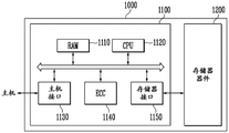
The controller 1100 includes a Random Access Memory (RAM)1110, a Central Processing Unit (CPU)1120, a host interface 1130, an Error Correction Code (ECC) circuit 1140, a memory interface 1150, and the like.
The RAM 1110 can be used as a work memory of the CPU 1120, a cache memory between the memory device 1200 and the host, and a buffer memory between the memory device 1200 and the host. The RAM 1110 may be replaced with a Static Random Access Memory (SRAM), a Read Only Memory (ROM), or the like.
The CPU 1120 is configured to control the overall operation of the controller 1100. For example, CPU 1120 is configured to operate firmware such as a Flash Translation Layer (FTL) stored in RAM 1110.
The host interface 1130 is configured to interact with a host. For example, the controller 1100 communicates with the host using at least one of various interface protocols, such as a Universal Serial Bus (USB) protocol, a multi-media card (MMC) protocol, a Peripheral Component Interconnect (PCI) protocol, a PCI-Express (PCI-E) protocol, an Advanced Technology Attachment (ATA) protocol, a serial ATA protocol, a parallel ATA protocol, a small computer system small interface (SCSI) protocol, an Enhanced Small Disk Interface (ESDI) protocol, an Integrated Drive Electronics (IDE) protocol, and a proprietary protocol.
The ECC circuit 1140 is configured to detect and correct errors included in data read from the memory device 1200 using an Error Correction Code (ECC).
The memory interface 1150 may be configured to interact with the memory device 1200. The memory interface 1150 includes a NAND interface or a NOR interface, for example.
The controller 1100 may further include a buffer memory (not shown) for temporarily storing data. The buffer memory may be used to temporarily store data transferred to the outside through the host interface 1130 or data transferred from the memory device 1200 through the memory interface 1150. The controller 1100 may further include a ROM storing code data for interacting with a host.
As described above, the memory system 1000 according to an embodiment of the present disclosure includes the memory device 1200 having an improved integration degree and improved characteristics, whereby the integration degree and characteristics of the memory system 1000 may be improved.
Fig. 7 is a block diagram showing a configuration of a memory system according to an embodiment of the present disclosure. Hereinafter, description of contents overlapping with the above will be omitted.
Referring to fig. 7, a memory system 1000 'according to an embodiment of the present disclosure includes a memory device 1200' and a controller 1100. The controller 1100 includes a RAM 1110, a CPU 1120, a host interface 1130, an ECC circuit 1140, a memory interface 1150, and the like.
The memory device 1200' may be a non-volatile memory. In addition, the memory device 1200' may have the structure described with reference to fig. 1A to 5D and be manufactured according to the manufacturing method described with reference to fig. 1A to 5D. In one embodiment, memory device 1200' may include: a stacked structure including a cell region and a contact region; a channel structure penetrating the cell region of the stacked structure; a trench penetrating a contact region of the stacked structure to reach different depths; and the stop structures penetrate through the contact areas of the stacked structures and are positioned between the grooves. The structure and manufacturing method of the memory device 1200' are the same as those described above, and thus a detailed description thereof will be omitted.
The memory device 1200' may be a multi-chip package including a plurality of memory chips. The plurality of memory chips are divided into a plurality of groups configured to communicate with the controller 1100 through the first to k-th channels (CH 1-CHk). In addition, the memory chips included in one group may be configured to communicate with the controller 1100 through a common channel. For reference, the memory system 1000' may be modified such that one memory chip is connected to one channel.
As described above, the memory system 1000 ' according to an embodiment of the present disclosure includes the memory device 1200 ' having an improved integration degree and improved characteristics, and thus the integration degree and characteristics of the memory system 1000 ' may be improved. In particular, the memory device 1200 ' is configured as a multi-chip package, so that the data storage capacity of the memory system 1000 ' can be increased and the operating speed of the memory system 1000 ' can be improved.
Fig. 8 is a block diagram illustrating a configuration of a computing system according to an embodiment of the present disclosure. Hereinafter, description of contents overlapping with the above will be omitted.
Referring to fig. 8, a computing system 2000 according to an embodiment of the present disclosure includes a memory device 2100, a CPU 2200, a RAM 2300, a user interface 2400, a power supply 2500, a system bus 2600, and the like.
The memory device 2100 stores data provided through the user interface 2400, data processed by the CPU 2200, and the like. Further, the memory device 2100 is electrically connected to the CPU 2200, the RAM 2300, the user interface 2400, the power supply 2500, and the like through the system bus 2600. For example, the memory device 2100 may be connected to the system bus 2600 by a controller (not shown) or directly. When the memory device 2100 is directly connected to the system bus 2600, the functions of the controller can be executed by the CPU 2200, the RAM 2300, or the like.
The memory device 2100 may be a non-volatile memory. In addition, the memory device 2100 may have the structure described with reference to fig. 1A to 5D and be manufactured according to the manufacturing method described with reference to fig. 1A to 5D. In one embodiment, the memory device 2100 may include: a stacked structure including a cell region and a contact region; a channel region penetrating the cell region of the stacked structure; a trench penetrating a contact region of the stacked structure to reach different depths; and the stop structures penetrate through the contact areas of the stacked structures and are positioned between the grooves. The structure and the manufacturing method of the memory device 2100 are the same as those described above, and thus a detailed description thereof will be omitted.
As described with reference to fig. 7, the memory device 2100 may be a multi-chip package including a plurality of memory chips.
The computing system 2000 configured as described above may be a computer, an ultra mobile pc (umpc), a workstation, a netbook, a Personal Digital Assistant (PDA), a portable computer, a web tablet, a wireless phone, a mobile phone, a smart phone, an electronic book, a Portable Multimedia Player (PMP), a portable game machine, a navigation device, a black box, a digital camera, a three-dimensional television, a digital audio recorder, a digital audio player, a digital image recorder, a digital image player, a digital video recorder, a digital video player, a device for transmitting information in a wireless environment, one of various electronic devices constituting a home network, one of various electronic devices constituting a computer network, one of various electronic devices constituting a telematics network, an RFID device, and the like.
As described above, the computing system 2000 according to the embodiment of the present disclosure includes the memory device 2100 having an improved degree of integration and improved characteristics, and thus characteristics of the computing system 2000 may also be improved.
Fig. 9 is a block diagram illustrating a configuration of a computing system according to an embodiment of the present disclosure.
Referring to FIG. 9, a computing system 3000 according to embodiments of the present disclosure includes software layers including an operating system 3200, applications 3100, a file system 3300, a translation layer 3400, and the like. Further, computing system 3000 includes hardware layers for memory device 3500 and the like.
The operating system 3200 may manage software resources, hardware resources, and the like of the computing system 3000, and control program execution by the central processing unit. The application 3100 is one of various application programs running on the computing system 3000, and may be a utility program executed by the operating system 3200.
The file system 3300 refers to a logical structure for managing data, files, and the like in the computing system 3000, and organizes the data or files stored in the memory device 3500 according to rules. The file system 3300 may be determined according to the operating system 3200 used in the computing system 3000. For example, when operating system 3200 is one of the Microsoft's Windows operating systems, file system 3300 may be the File Allocation Table (FAT) or the NT file system (NTFS). When operating system 3200 is one of the Unix/Linux operating systems, file system 3300 may be an extended file system (EXT), a Unix File System (UFS), or a Journaling File System (JFS).
In this figure, the operating system 3200, the application 3100 and the file system 3300 are shown as separate blocks. However, the application 3100 and the file system 3300 may be included in the operating system 3200.
The translation layer 3400 converts the address into a form suitable for the memory device 3500 in response to a request from the file system 3300. For example, the translation layer 3400 translates logical addresses generated by the file system 3300 to physical addresses of the memory device 3500. The mapping information between the logical address and the physical address may be stored as an address translation table. For example, translation layer 3400 may be a Flash Translation Layer (FTL), a universal flash link layer (ULL), or the like.
The memory device 3500 may be a non-volatile memory. In addition, the memory device 3500 may have the structure described with reference to fig. 1A to 5D, and be manufactured according to the manufacturing method described with reference to fig. 1A to 5D. In one embodiment, memory device 3500 may include: a stacked structure including a cell region and a contact region; a channel structure penetrating the cell region of the stacked structure; a trench penetrating a contact region of the stacked structure to different depths; and the stop structures penetrate through the contact areas of the stacked structures and are positioned between the grooves. The structure and manufacturing method of the memory device 3500 are the same as those described above, and thus a detailed description thereof will be omitted.
The computing system 3000 configured as described above can be divided into an operating system layer executed in an upper layer area and a controller layer executed in a lower layer area. The application 3100, operating system 3200, and file system 3300 are included in the operating system layer, and may be driven by working memory of the computing system 3000. Further, the conversion layer 3400 may be included in an operating system layer or a controller layer.
As described above, the computing system 3000 according to the embodiment of the present disclosure includes the storage device 3500 having an improved integration degree and improved characteristics, and thus characteristics of the computing system 3000 may also be improved.
According to the present disclosure, a semiconductor device having a stable structure and improved reliability can be provided. In addition, when the semiconductor device is manufactured, the process difficulty can be reduced, the manufacturing process can be simplified, and the manufacturing cost can be reduced.
Examples of the disclosed embodiments are described in the drawings and specification. Although specific terms are employed herein, these terms are merely used to explain embodiments of the disclosure. Accordingly, the present disclosure is not limited to the above-described embodiments, and many variations may be made within the spirit and scope of the present disclosure. It should be apparent to those skilled in the art that various modifications can be made based on the technical scope of the present disclosure in addition to the embodiments disclosed herein.
All terms (including technical and scientific terms) used herein have the same meaning as commonly understood by one of ordinary skill in the art to which this invention belongs, without differing definitions. It is to be understood that the terms defined in the dictionary have their meanings consistent with the context of the relevant art. Terms are not to be interpreted in an idealized or overly formal sense as not expressly defined herein.
Claims (28)
1. A semiconductor device, comprising:
a stacked structure including a cell region and a contact region;
a channel structure penetrating the cell region of the stack structure;
a trench penetrating the contact region of the stacked structure to reach a different depth; and
a stop structure penetrating the contact region of the stacked structure, the stop structure being located between the trenches.
2. The semiconductor device of claim 1, wherein regions of the stacked structure between the trenches and within the contact region have a uniform height.
3. The semiconductor device of claim 1, wherein the stop structure comprises:
a dummy channel layer penetrating the stack structure.
4. The semiconductor device of claim 3, wherein the stop structure comprises:
a dummy memory layer surrounding a sidewall of the dummy channel layer; and
a dummy gap-fill layer in the dummy channel layer.
5. The semiconductor device of claim 3, wherein sidewalls of the dummy channel layer comprise at least one turning point.
6. The semiconductor device of claim 1, wherein the stop structure comprises:
a contact plug penetrating the stacked structure; and
and an insulating spacer surrounding sidewalls of the contact plug.
7. The semiconductor device of claim 1, further comprising an insulating pattern formed in the trench.
8. The semiconductor device according to claim 7, wherein an upper surface of the insulating pattern and an upper surface of the stop structure are located at substantially the same level.
9. The semiconductor device of claim 1, wherein the stop structure penetrates the stack structure to a partial depth.
10. A semiconductor device, comprising:
a first sub-stack structure;
a second sub-stacking structure located on the first sub-stacking structure;
a channel structure including a first sub-channel structure penetrating the first sub-stack structure and a second sub-channel structure penetrating the second sub-stack structure;
a trench penetrating the second sub-stack structure to reach a different depth; and
a stop structure penetrating the second sub-stack structure, the stop structure being located between the trenches.
11. The semiconductor device of claim 10, wherein regions of the second sub-stacked structure between the trenches have a uniform height.
12. The semiconductor device of claim 10, wherein the stop structure and the second sub-channel structure have substantially the same height.
13. The semiconductor device of claim 10, wherein the stop structure comprises:
a dummy channel layer penetrating the second sub-stack structure;
a dummy memory layer surrounding a sidewall of the dummy channel layer; and
a dummy gap-fill layer in the dummy channel layer.
14. The semiconductor device of claim 10, wherein the stop structure comprises:
a contact plug penetrating the second sub-stack structure; and
and an insulating spacer surrounding sidewalls of the contact plug.
15. The semiconductor device of claim 10, further comprising an insulating pattern formed in the trench.
16. The semiconductor device according to claim 15, wherein an upper surface of the insulating pattern and an upper surface of the stop structure are located at substantially the same level.
17. A method of manufacturing a semiconductor device, the method comprising:
forming a stacked structure including a cell region and a contact region;
forming a channel structure penetrating the cell region of the stack structure;
forming a stop structure penetrating the contact region of the stacked structure;
forming trenches penetrating the contact regions of the stacked structures to reach different depths, the trenches being located between the stop structures;
forming an insulating material on the stacked structure including the trench; and
forming an insulating pattern in the trench by planarizing the insulating material using the stop structure.
18. The method of claim 17, wherein the stop structure is formed when forming the channel structure.
19. The method of claim 17, wherein the stop structure comprises a material having a higher etch selectivity relative to the stack structure.
20. The method of claim 17, wherein regions of the stacked structure between the trenches have a uniform height.
21. The method of claim 17, wherein each of the stop structures comprises:
a dummy channel layer penetrating the stack structure;
a dummy memory layer surrounding a sidewall of the dummy channel layer; and
a dummy gap-fill layer in the dummy channel layer.
22. The method of claim 17, wherein each of the stop structures comprises:
a contact plug penetrating the stacked structure; and
and an insulating spacer surrounding sidewalls of the contact plug.
23. A method of manufacturing a semiconductor device, the method comprising:
forming a first sub-stack structure;
forming a first sub-channel structure penetrating the first sub-stacked structure;
forming a second sub-stacked structure on the first sub-stacked structure;
forming a second sub-channel structure penetrating through the second sub-stacked structure;
forming a stop structure penetrating the second sub-stacked structure when the second sub-channel structure is formed; and
forming trenches penetrating the second sub-stack structure to reach different depths, the trenches being located between the stop structures.
24. The method of claim 23, wherein the first sub-channel structure is formed while forming the second sub-channel structure.
25. The method of claim 23, wherein the first sub-channel structure is formed prior to forming the second sub-stack structure.
26. The method of claim 23, further comprising:
forming an insulating material on the second sub-stack structure including the trench; and
forming an insulating pattern in the trench by planarizing the insulating material using the stop structure.
27. The method of claim 23, wherein the stop structure comprises a material having a higher etch selectivity relative to the second sub-stack structure.
28. The method of claim 23, wherein regions of the second sub-stacked structure between the trenches have a uniform height.
Applications Claiming Priority (2)
| Application Number | Priority Date | Filing Date | Title |
|---|---|---|---|
| KR10-2019-0118246 | 2019-09-25 | ||
| KR1020190118246A KR102701565B1 (en) | 2019-09-25 | 2019-09-25 | Semiconductor device and manufacturing method of semiconductor device |
Publications (2)
| Publication Number | Publication Date |
|---|---|
| CN112563280A true CN112563280A (en) | 2021-03-26 |
| CN112563280B CN112563280B (en) | 2024-06-11 |
Family
ID=74881178
Family Applications (1)
| Application Number | Title | Priority Date | Filing Date |
|---|---|---|---|
| CN202010561455.6A Active CN112563280B (en) | 2019-09-25 | 2020-06-18 | Semiconductor device and method for manufacturing the same |
Country Status (3)
| Country | Link |
|---|---|
| US (1) | US11574920B2 (en) |
| KR (1) | KR102701565B1 (en) |
| CN (1) | CN112563280B (en) |
Families Citing this family (3)
| Publication number | Priority date | Publication date | Assignee | Title |
|---|---|---|---|---|
| US11765916B2 (en) * | 2020-06-17 | 2023-09-19 | Kioxia Corporation | Memory device and method of manufacturing memory device |
| US12406926B2 (en) | 2021-08-30 | 2025-09-02 | Micron Technology, Inc. | Microelectronic devices including stadium structures |
| KR20240072706A (en) * | 2022-11-17 | 2024-05-24 | 에스케이하이닉스 주식회사 | Memory device and manufacturing method of the memory device |
Citations (13)
| Publication number | Priority date | Publication date | Assignee | Title |
|---|---|---|---|---|
| US20100133599A1 (en) * | 2008-12-03 | 2010-06-03 | Samsung Electronics Co., Ltd. | Nonvolatile memory device and method for fabricating the same |
| KR20100097459A (en) * | 2009-02-26 | 2010-09-03 | 삼성전자주식회사 | Method for fabricating nonvolatile memory devices |
| US20120003831A1 (en) * | 2010-07-05 | 2012-01-05 | Daehyuk Kang | Methods of Forming Nonvolatile Memory Devices Using Nonselective and Selective Etching Techniques to Define Vertically Stacked Word Lines |
| US20150340376A1 (en) * | 2014-05-20 | 2015-11-26 | Jintaek Park | Semiconductor device and method of fabricating the same |
| US9356043B1 (en) * | 2015-06-22 | 2016-05-31 | Sandisk Technologies Inc. | Three-dimensional memory devices containing memory stack structures with position-independent threshold voltage |
| US20160218059A1 (en) * | 2015-01-22 | 2016-07-28 | SanDisk Technologies, Inc. | Composite contact via structure containing an upper portion which fills a cavity within a lower portion |
| US20170263556A1 (en) * | 2016-03-11 | 2017-09-14 | Micron Technology, Inc. | Conductive structures, systems and devices including conductive structures and related methods |
| US20180286678A1 (en) * | 2017-03-30 | 2018-10-04 | SK Hynix Inc. | Semiconductor device and method for manufacturing the same |
| CN108962895A (en) * | 2017-05-26 | 2018-12-07 | 美光科技公司 | Semiconductor device, electronic system and the method for forming semiconductor device structure |
| CN109075175A (en) * | 2016-06-07 | 2018-12-21 | 桑迪士克科技有限责任公司 | Straight-through storage level through-hole structure between staircase areas in three-dimensional memory devices and preparation method thereof |
| US20190139974A1 (en) * | 2017-11-07 | 2019-05-09 | Sandisk Technologies Llc | Three-dimensional memory device having level-shifted staircases and method of making thereof |
| DE102018123386A1 (en) * | 2017-12-08 | 2019-06-13 | Samsung Electronics Co., Ltd. | Three-dimensional semiconductor memory devices and methods for their manufacture |
| CN110098188A (en) * | 2018-01-31 | 2019-08-06 | 三星电子株式会社 | Semiconductor device |
Family Cites Families (5)
| Publication number | Priority date | Publication date | Assignee | Title |
|---|---|---|---|---|
| US9627403B2 (en) | 2015-04-30 | 2017-04-18 | Sandisk Technologies Llc | Multilevel memory stack structure employing support pillar structures |
| KR20170014757A (en) | 2015-07-31 | 2017-02-08 | 에스케이하이닉스 주식회사 | Semiconductor device and manufacturing method of the same |
| KR102415206B1 (en) * | 2016-06-27 | 2022-07-01 | 에스케이하이닉스 주식회사 | Semiconductor device |
| KR102612195B1 (en) * | 2018-06-11 | 2023-12-12 | 삼성전자주식회사 | Semiconductor devices and manufacturing methods of the same |
| KR102807776B1 (en) * | 2020-02-28 | 2025-05-14 | 삼성전자주식회사 | Vertical memory devices |
-
2019
- 2019-09-25 KR KR1020190118246A patent/KR102701565B1/en active Active
-
2020
- 2020-05-11 US US16/872,032 patent/US11574920B2/en active Active
- 2020-06-18 CN CN202010561455.6A patent/CN112563280B/en active Active
Patent Citations (14)
| Publication number | Priority date | Publication date | Assignee | Title |
|---|---|---|---|---|
| US20100133599A1 (en) * | 2008-12-03 | 2010-06-03 | Samsung Electronics Co., Ltd. | Nonvolatile memory device and method for fabricating the same |
| KR20100097459A (en) * | 2009-02-26 | 2010-09-03 | 삼성전자주식회사 | Method for fabricating nonvolatile memory devices |
| US20120003831A1 (en) * | 2010-07-05 | 2012-01-05 | Daehyuk Kang | Methods of Forming Nonvolatile Memory Devices Using Nonselective and Selective Etching Techniques to Define Vertically Stacked Word Lines |
| US20150340376A1 (en) * | 2014-05-20 | 2015-11-26 | Jintaek Park | Semiconductor device and method of fabricating the same |
| US20160218059A1 (en) * | 2015-01-22 | 2016-07-28 | SanDisk Technologies, Inc. | Composite contact via structure containing an upper portion which fills a cavity within a lower portion |
| US9356043B1 (en) * | 2015-06-22 | 2016-05-31 | Sandisk Technologies Inc. | Three-dimensional memory devices containing memory stack structures with position-independent threshold voltage |
| US20170263556A1 (en) * | 2016-03-11 | 2017-09-14 | Micron Technology, Inc. | Conductive structures, systems and devices including conductive structures and related methods |
| CN109075175A (en) * | 2016-06-07 | 2018-12-21 | 桑迪士克科技有限责任公司 | Straight-through storage level through-hole structure between staircase areas in three-dimensional memory devices and preparation method thereof |
| US20180286678A1 (en) * | 2017-03-30 | 2018-10-04 | SK Hynix Inc. | Semiconductor device and method for manufacturing the same |
| CN108695335A (en) * | 2017-03-30 | 2018-10-23 | 爱思开海力士有限公司 | Semiconductor device and its manufacturing method |
| CN108962895A (en) * | 2017-05-26 | 2018-12-07 | 美光科技公司 | Semiconductor device, electronic system and the method for forming semiconductor device structure |
| US20190139974A1 (en) * | 2017-11-07 | 2019-05-09 | Sandisk Technologies Llc | Three-dimensional memory device having level-shifted staircases and method of making thereof |
| DE102018123386A1 (en) * | 2017-12-08 | 2019-06-13 | Samsung Electronics Co., Ltd. | Three-dimensional semiconductor memory devices and methods for their manufacture |
| CN110098188A (en) * | 2018-01-31 | 2019-08-06 | 三星电子株式会社 | Semiconductor device |
Also Published As
| Publication number | Publication date |
|---|---|
| KR102701565B1 (en) | 2024-09-04 |
| KR20210036144A (en) | 2021-04-02 |
| US20210091109A1 (en) | 2021-03-25 |
| CN112563280B (en) | 2024-06-11 |
| US11574920B2 (en) | 2023-02-07 |
Similar Documents
| Publication | Publication Date | Title |
|---|---|---|
| US12048168B2 (en) | Three-dimensional semiconductor device | |
| US10643844B2 (en) | Semiconductor device and method for manufacturing the same | |
| US11037939B2 (en) | Semiconductor device and method of manufacturing the same | |
| US10930666B2 (en) | Semiconductor device and method of manufacturing the same | |
| US10644026B2 (en) | Semiconductor device and manufacturing method thereof | |
| US10985180B2 (en) | Semiconductor device and manufacturing method thereof | |
| KR102535100B1 (en) | Semiconductor device and method for manufacturing the same | |
| KR20180106727A (en) | Semiconductor device and manufacturing method of the same | |
| US20240414920A1 (en) | Semiconductor device and manufacturing method of the semiconductor device | |
| US20250089246A1 (en) | Semiconductor device and a method of manufacturing a semiconductor device | |
| US11751390B2 (en) | Manufacturing method of semiconductor device including stepping structure and supporting structure | |
| CN112563280B (en) | Semiconductor device and method for manufacturing the same | |
| KR20250127026A (en) | Semiconductor device and manufacturing method thereof | |
| CN112420597B (en) | Method for manufacturing semiconductor device | |
| KR102891356B1 (en) | Semiconductor device and manufacturing method of semiconductor device | |
| CN115696926A (en) | Semiconductor device and method of manufacturing the same | |
| KR20220120974A (en) | Memory device and manufacturing method thereof |
Legal Events
| Date | Code | Title | Description |
|---|---|---|---|
| PB01 | Publication | ||
| PB01 | Publication | ||
| SE01 | Entry into force of request for substantive examination | ||
| SE01 | Entry into force of request for substantive examination | ||
| GR01 | Patent grant | ||
| GR01 | Patent grant |