CN112491267B - Common-ground BUCK constant current driving circuit and multi-output switching power supply - Google Patents

Common-ground BUCK constant current driving circuit and multi-output switching power supply Download PDF

Info

Publication number
CN112491267B
CN112491267B CN202011217402.9A CN202011217402A CN112491267B CN 112491267 B CN112491267 B CN 112491267B CN 202011217402 A CN202011217402 A CN 202011217402A CN 112491267 B CN112491267 B CN 112491267B
Authority
CN
China
Prior art keywords
buck
circuit
constant current
twenty
current control
Prior art date
Legal status (The legal status is an assumption and is not a legal conclusion. Google has not performed a legal analysis and makes no representation as to the accuracy of the status listed.)
Active
Application number
CN202011217402.9A
Other languages
Chinese (zh)
Other versions
CN112491267A (en
Inventor
王宗友
郭怀峰
Current Assignee (The listed assignees may be inaccurate. Google has not performed a legal analysis and makes no representation or warranty as to the accuracy of the list.)
Guangdong Songsheng Power Technology Co ltd
Original Assignee
Shenzhen Sosen Electronics Co Ltd
Priority date (The priority date is an assumption and is not a legal conclusion. Google has not performed a legal analysis and makes no representation as to the accuracy of the date listed.)
Filing date
Publication date
Application filed by Shenzhen Sosen Electronics Co Ltd filed Critical Shenzhen Sosen Electronics Co Ltd
Priority to CN202011217402.9A priority Critical patent/CN112491267B/en
Publication of CN112491267A publication Critical patent/CN112491267A/en
Application granted granted Critical
Publication of CN112491267B publication Critical patent/CN112491267B/en
Active legal-status Critical Current
Anticipated expiration legal-status Critical

Links

Images

Classifications

    • HELECTRICITY
    • H02GENERATION; CONVERSION OR DISTRIBUTION OF ELECTRIC POWER
    • H02MAPPARATUS FOR CONVERSION BETWEEN AC AND AC, BETWEEN AC AND DC, OR BETWEEN DC AND DC, AND FOR USE WITH MAINS OR SIMILAR POWER SUPPLY SYSTEMS; CONVERSION OF DC OR AC INPUT POWER INTO SURGE OUTPUT POWER; CONTROL OR REGULATION THEREOF
    • H02M3/00Conversion of DC power input into DC power output
    • H02M3/02Conversion of DC power input into DC power output without intermediate conversion into AC
    • H02M3/04Conversion of DC power input into DC power output without intermediate conversion into AC by static converters
    • H02M3/10Conversion of DC power input into DC power output without intermediate conversion into AC by static converters using discharge tubes with control electrode or semiconductor devices with control electrode
    • H02M3/145Conversion of DC power input into DC power output without intermediate conversion into AC by static converters using discharge tubes with control electrode or semiconductor devices with control electrode using devices of a triode or transistor type requiring continuous application of a control signal
    • H02M3/155Conversion of DC power input into DC power output without intermediate conversion into AC by static converters using discharge tubes with control electrode or semiconductor devices with control electrode using devices of a triode or transistor type requiring continuous application of a control signal using semiconductor devices only
    • H02M3/156Conversion of DC power input into DC power output without intermediate conversion into AC by static converters using discharge tubes with control electrode or semiconductor devices with control electrode using devices of a triode or transistor type requiring continuous application of a control signal using semiconductor devices only with automatic control of output voltage or current, e.g. switching regulators
    • HELECTRICITY
    • H02GENERATION; CONVERSION OR DISTRIBUTION OF ELECTRIC POWER
    • H02HEMERGENCY PROTECTIVE CIRCUIT ARRANGEMENTS
    • H02H7/00Emergency protective circuit arrangements specially adapted for specific types of electric machines or apparatus or for sectionalised protection of cable or line systems, and effecting automatic switching in the event of an undesired change from normal working conditions
    • H02H7/10Emergency protective circuit arrangements specially adapted for specific types of electric machines or apparatus or for sectionalised protection of cable or line systems, and effecting automatic switching in the event of an undesired change from normal working conditions for converters; for rectifiers
    • H02H7/12Emergency protective circuit arrangements specially adapted for specific types of electric machines or apparatus or for sectionalised protection of cable or line systems, and effecting automatic switching in the event of an undesired change from normal working conditions for converters; for rectifiers for static converters or rectifiers
    • H02H7/1213Emergency protective circuit arrangements specially adapted for specific types of electric machines or apparatus or for sectionalised protection of cable or line systems, and effecting automatic switching in the event of an undesired change from normal working conditions for converters; for rectifiers for static converters or rectifiers for DC-DC converters
    • HELECTRICITY
    • H05ELECTRIC TECHNIQUES NOT OTHERWISE PROVIDED FOR
    • H05BELECTRIC HEATING; ELECTRIC LIGHT SOURCES NOT OTHERWISE PROVIDED FOR; CIRCUIT ARRANGEMENTS FOR ELECTRIC LIGHT SOURCES, IN GENERAL
    • H05B45/00Circuit arrangements for operating light-emitting diodes [LED]
    • H05B45/30Driver circuits
    • H05B45/345Current stabilisation; Maintaining constant current
    • HELECTRICITY
    • H05ELECTRIC TECHNIQUES NOT OTHERWISE PROVIDED FOR
    • H05BELECTRIC HEATING; ELECTRIC LIGHT SOURCES NOT OTHERWISE PROVIDED FOR; CIRCUIT ARRANGEMENTS FOR ELECTRIC LIGHT SOURCES, IN GENERAL
    • H05B45/00Circuit arrangements for operating light-emitting diodes [LED]
    • H05B45/30Driver circuits
    • H05B45/37Converter circuits
    • H05B45/3725Switched mode power supply [SMPS]
    • HELECTRICITY
    • H05ELECTRIC TECHNIQUES NOT OTHERWISE PROVIDED FOR
    • H05BELECTRIC HEATING; ELECTRIC LIGHT SOURCES NOT OTHERWISE PROVIDED FOR; CIRCUIT ARRANGEMENTS FOR ELECTRIC LIGHT SOURCES, IN GENERAL
    • H05B45/00Circuit arrangements for operating light-emitting diodes [LED]
    • H05B45/50Circuit arrangements for operating light-emitting diodes [LED] responsive to malfunctions or undesirable behaviour of LEDs; responsive to LED life; Protective circuits
    • YGENERAL TAGGING OF NEW TECHNOLOGICAL DEVELOPMENTS; GENERAL TAGGING OF CROSS-SECTIONAL TECHNOLOGIES SPANNING OVER SEVERAL SECTIONS OF THE IPC; TECHNICAL SUBJECTS COVERED BY FORMER USPC CROSS-REFERENCE ART COLLECTIONS [XRACs] AND DIGESTS
    • Y02TECHNOLOGIES OR APPLICATIONS FOR MITIGATION OR ADAPTATION AGAINST CLIMATE CHANGE
    • Y02BCLIMATE CHANGE MITIGATION TECHNOLOGIES RELATED TO BUILDINGS, e.g. HOUSING, HOUSE APPLIANCES OR RELATED END-USER APPLICATIONS
    • Y02B20/00Energy efficient lighting technologies, e.g. halogen lamps or gas discharge lamps
    • Y02B20/30Semiconductor lamps, e.g. solid state lamps [SSL] light emitting diodes [LED] or organic LED [OLED]

Landscapes

  • Engineering & Computer Science (AREA)
  • Power Engineering (AREA)
  • Circuit Arrangement For Electric Light Sources In General (AREA)
  • Dc-Dc Converters (AREA)

Abstract

本发明涉及一种可共地的BUCK恒流驱动电路及多路输出开关电源,包括:BUCK输入检测转换电路、BUCK恒流控制单元、BUCK储能电路、BUCK续流电路、短路处理电路、以及采样电路;BUCK输入检测转换电路的第一端接入输入信号,BUCK输入检测转换电路的第二端连接BUCK恒流控制单元的输入端,BUCK输入检测转换电路的第三端通过采样电路连接至BUCK恒流控制单元的采样端,BUCK恒流控制单元的输出端连接BUCK储能电路的输入端,BUCK储能电路的输出端输出驱动信号;BUCK续流电路与BUCK储能电路连接,短路处理电路分别与BUCK续流电路和采样电路连接、以在输出端短路时通过采样电路输出反馈信号至BUCK恒流控制单元。本发明的驱动电路输入和输出可共地,可有效减少布线,解决布线难、成本高的问题。

Figure 202011217402

The invention relates to a buck constant current drive circuit and a multi-channel output switching power supply that can share the ground, comprising: a buck input detection conversion circuit, a buck constant current control unit, a buck energy storage circuit, a buck freewheeling circuit, a short circuit processing circuit, and Sampling circuit; the first end of the BUCK input detection conversion circuit is connected to the input signal, the second end of the BUCK input detection conversion circuit is connected to the input end of the BUCK constant current control unit, and the third end of the BUCK input detection conversion circuit is connected to the sampling circuit through the sampling circuit. The sampling end of the BUCK constant current control unit, the output end of the BUCK constant current control unit is connected to the input end of the BUCK energy storage circuit, and the output end of the BUCK energy storage circuit outputs the driving signal; the BUCK freewheeling circuit is connected to the BUCK energy storage circuit, short-circuit processing The circuit is respectively connected with the buck freewheeling circuit and the sampling circuit, so as to output a feedback signal to the buck constant current control unit through the sampling circuit when the output end is short-circuited. The input and output of the driving circuit of the present invention can share the ground, which can effectively reduce wiring and solve the problems of difficult wiring and high cost.

Figure 202011217402

Description

Common-ground BUCK constant current driving circuit and multi-output switching power supply
Technical Field
The invention relates to the technical field of driving power supplies, in particular to a common-ground BUCK constant-current driving circuit and a multi-output switching power supply.
Background
The LED lighting has the outstanding advantages of energy conservation, high light efficiency and the like, so the LED lighting is widely applied to various lighting places. Various lighting circuit topologies are applied to an LED switching power supply, the requirement of people on light is higher and higher, light sources of various colors are demanded by people, especially in some lighting projects, the color change of different light sources needs to be controlled, so that a plurality of driving power supplies are needed to drive the light sources of different colors, rather than simply connecting the light sources in series and parallel, and therefore, the current market has several application schemes:
1. one-to-one, one AD-DC power supply drives one or a part of light sources, and then the whole engineering application has a great number of AD-DC components, which obviously has high cost and is not suitable for engineering application;
2. one is more, namely a high-power AC-DC constant voltage source, and then a very large number of DC-DC direct current power supplies are provided behind the AC-DC constant voltage source, and the scheme is also a mainstream scheme in the market, because most DC-DC control chips have high working frequency, the DC-DC constant voltage source has the advantages of low cost and small volume;
however, the output of the current DC-DC constant current conversion chip cannot be connected to the input common ground, in the lighting engineering, many DC-DC modules often drive different color light sources, and if the output cannot be connected to the common ground, each color function module will be connected to four wires, which are Vin +, Vin-, LED +, LED-. When the number of color function modules to be driven is larger, more wiring is needed, which causes the problems of excessive wiring, difficult wiring and high cost in practical engineering application.
Disclosure of Invention
The present invention is directed to provide a BUCK constant current driving circuit and a multi-output switching power supply, which can be commonly grounded.
The technical scheme adopted by the invention for solving the technical problems is as follows: a common-ground BUCK constant current driving circuit is constructed, and comprises: the BUCK input detection conversion circuit, the BUCK constant current control unit, the BUCK energy storage circuit, the BUCK follow current circuit, the short circuit processing circuit and the sampling circuit;
the first end of the BUCK input detection conversion circuit is connected with an input signal, the second end of the BUCK input detection conversion circuit is connected with the input end of the BUCK constant current control unit, the third end of the BUCK input detection conversion circuit is connected with the sampling end of the BUCK constant current control unit through the sampling circuit, the output end of the BUCK constant current control unit is connected with the input end of the BUCK energy storage circuit, and the output end of the BUCK energy storage circuit outputs a driving signal;
the BUCK follow current circuit is connected with the BUCK energy storage circuit, and the short-circuit processing circuit is respectively connected with the BUCK follow current circuit and the sampling circuit so as to output a feedback signal to the BUCK constant current control unit through the sampling circuit when the output end is short-circuited.
Preferably, the method further comprises the following steps: and the filter circuit is arranged between the sampling end of the BUCK constant current control unit and the sampling circuit.
Preferably, the method further comprises the following steps: and the overvoltage protection circuit is arranged at the output end and is connected with the sampling end of the BUCK constant current control unit.
Preferably, the BUCK input detection conversion circuit includes: a second current transformer;
the first end of the primary winding of the second current transformer is connected with an input signal, the second end of the primary winding of the second current transformer is connected with the input end of the BUCK constant current control unit, the first end of the secondary winding of the second current transformer is connected with the sampling circuit, and the second end of the secondary winding of the second current transformer is grounded.
Preferably, the BUCK constant current control unit includes: a BUCK constant current control chip;
an eighth pin of the BUCK constant current control chip is used as an input end of the BUCK constant current control unit and connected with a second end of a primary winding of the second current transformer, a first pin of the BUCK constant current control chip is used as an output end of the BUCK constant current control unit and connected with an input end of the BUCK energy storage circuit, and a fifth pin of the BUCK constant current control chip is used as a sampling end of the BUCK constant current control unit and connected with the filter circuit.
Preferably, the BUCK tank circuit comprises: a first inductor;
the first end of the first inductor is used as the input end of the BUCK energy storage circuit and connected with the first pin of the BUCK constant current control chip, and the second end of the first inductor is used as the output end of the BUCK energy storage circuit to output the driving signal.
Preferably, the sampling circuit includes: a twenty-first diode, a twenty-fifth resistor and a twenty-fifth capacitor;
a first end of the twenty-first diode is connected with a first end of a secondary winding of the second current transformer, a second end of the twenty-first diode is connected with the short-circuit processing circuit, and a third end of the twenty-first diode is connected with the filter circuit;
the first end of the twenty-fifth resistor is connected with the third end of the twenty-first diode, the second end of the twenty-fifth resistor is grounded, and the twenty-fifth capacitor is connected with the twenty-fifth resistor in parallel.
Preferably, the filter circuit includes: a twenty-third resistor and a twenty-fourth capacitor;
the second end of the twenty-third resistor is connected with the third end of the twenty-first diode, the first end of the twenty-third resistor is connected with the first end of the twenty-fourth capacitor and connected to the fifth pin of the BUCK constant current control chip, and the second end of the twenty-fourth capacitor is grounded.
Preferably, the BUCK freewheel circuit includes: a twenty-second diode and a primary winding of a third current transformer; the short circuit processing circuit includes: a secondary winding of the third current transformer;
the cathode of the twenty-second diode is connected with the first end of the first inductor, the anode of the twenty-second diode is connected with the second end of the primary winding of the third current transformer, and the first end of the primary winding of the third current transformer is grounded.
The present invention also provides a multiple output switching power supply, comprising: at least one BUCK constant current driving circuit which can be connected with the ground in common.
The implementation of the common-ground BUCK constant-current driving circuit and the multi-output switching power supply has the following beneficial effects: the method comprises the following steps: the BUCK input detection conversion circuit, the BUCK constant current control unit, the BUCK energy storage circuit, the BUCK follow current circuit, the short circuit processing circuit and the sampling circuit; the first end of the BUCK input detection conversion circuit is connected with an input signal, the second end of the BUCK input detection conversion circuit is connected with the input end of the BUCK constant current control unit, the third end of the BUCK input detection conversion circuit is connected to the sampling end of the BUCK constant current control unit through the sampling circuit, the output end of the BUCK constant current control unit is connected with the input end of the BUCK energy storage circuit, and the output end of the BUCK energy storage circuit outputs a driving signal; the BUCK follow current circuit is connected with the BUCK energy storage circuit, and the short circuit processing circuit is respectively connected with the BUCK follow current circuit and the sampling circuit so as to output a feedback signal to the BUCK constant current control unit through the sampling circuit when the output end is short-circuited. The input and the output of the driving circuit can be commonly grounded, wiring can be effectively reduced, and the problems of difficult wiring and high cost are solved.
Drawings
The invention will be further described with reference to the accompanying drawings and examples, in which:
FIG. 1 is a schematic block diagram of a common-ground BUCK constant current driving circuit provided by an embodiment of the invention;
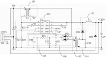
FIG. 2 is a schematic circuit diagram of a common-ground BUCK constant current driving circuit according to an embodiment of the present invention;
fig. 3 is a schematic block diagram of a multiple-output switching power supply according to an embodiment of the present invention.
Detailed Description
For a more clear understanding of the technical features, objects and effects of the present invention, embodiments of the present invention will now be described in detail with reference to the accompanying drawings.
Referring to fig. 1, fig. 1 is a schematic block diagram of an alternative embodiment of each example of the common-ground BUCK constant current driving circuit provided in the present invention. The common ground BUCK constant current driving circuit can be applied to the technical field of driving, such as the technical field of LED driving.
As shown in fig. 1, the common-grounded BUCK constant current driving circuit comprises: the BUCK input detection conversion circuit 101, the BUCK constant current control unit 102, the BUCK tank circuit 103, the BUCK freewheel circuit 104, the short-circuit processing circuit 105, and the sampling circuit 106.
A first end of the BUCK input detection conversion circuit 101 is connected with an input signal, a second end of the BUCK input detection conversion circuit 101 is connected with an input end of the BUCK constant current control unit 102, a third end of the BUCK input detection conversion circuit 101 is connected with a sampling end of the BUCK constant current control unit 102 through a sampling circuit 106, an output end of the BUCK constant current control unit 102 is connected with an input end of the BUCK energy storage circuit 103, and an output end of the BUCK energy storage circuit 103 outputs a driving signal; the BUCK flywheel circuit 104 is connected with the BUCK energy storage circuit 103, and the short-circuit processing circuit 105 is respectively connected with the BUCK flywheel circuit 104 and the sampling circuit 106 to output a feedback signal to the BUCK constant-current control unit 102 through the sampling circuit 106 when the output end is short-circuited.
Further, in this embodiment, the common-ground-capable BUCK constant current driving circuit may further include: and the filter circuit 107 is arranged between the sampling end of the BUCK constant current control unit 102 and the sampling circuit 106. The filter circuit 107 can filter the signal output by the sampling circuit 106 and then transmit the signal to the BUCK constant current control unit 102, so that the BUCK constant current control unit 102 can receive the stable sampling signal.
At the moment of power-on, an input signal flows into the BUCK input detection conversion circuit 101, the BUCK input detection conversion circuit 101 receives an input current in the input signal and transmits the input current to the BUCK constant current control unit 102, so that the BUCK constant current control unit 102 is turned on and outputs a current to the BUCK energy storage circuit 103, and the BUCK energy storage circuit 103 stores energy and outputs a driving signal to a load (such as an LED lamp, an LED lamp bead, an LED lamp string and the like) to start the load (such as lighting the LED lamp).
After the power-on, the BUCK input detection conversion circuit 101 further amplifies a voltage signal in the input signal, the amplified voltage signal is sampled by the sampling circuit 106, filtered by the filter circuit 107 and transmitted to the BUCK constant current control unit 102, and the BUCK constant current control unit 102 stops outputting the energy storage circuit after receiving the signal and stops storing energy in the energy storage circuit.
Since the energy storage of the energy storage circuit is completed in the previous stage and the energy storage circuit needs to be released, after the BUCK constant current control unit 102 stops storing energy to the energy storage circuit, the energy storage circuit and the BUCK follow current loop form follow current to continuously provide electric energy to the load.
Further, when the output end is short-circuited, due to the effect of the short-circuit processing circuit 105, the short-circuit signal can be output to the sampling circuit 106 through the short-circuit processing circuit 105 to be sampled by the sampling circuit 106, processed by the filter circuit 107 and transmitted to the BUCK constant-current control unit 102, so that the BUCK constant-current control unit 102 turns off an internal switching tube, the BUCK constant-current control unit 102 is prevented from being damaged, and the purpose of short-circuit protection is achieved.
The BUCK flywheel circuit 104 and the short-circuit processing circuit 105 in the embodiment of the invention are isolated from each other, that is, by providing the BUCK flywheel circuit 104 and the short-circuit processing circuit 105 which are isolated from each other, the BUCK constant current driving circuit of the invention can realize common input and output, thereby reducing the wiring in actual operation and reducing the wiring cost.
Further, in this embodiment, the common-ground-capable BUCK constant current driving circuit may further include: and the overvoltage protection circuit is arranged at the output end and is connected with the sampling end of the BUCK constant current control unit 102. Specifically, when the output end has an overvoltage phenomenon, overvoltage protection can be realized through the overvoltage protection circuit, so that the device is prevented from being damaged, and the power supply is further damaged.
Fig. 2 is a schematic circuit diagram of an alternative embodiment of the common ground BUCK constant current driving circuit according to the present invention.
Specifically, as shown in fig. 2, the BUCK input detection conversion circuit 101 includes: a second current transformer T2;
a first end of a primary winding of the second current transformer T2 is connected with an input signal, a second end of a primary winding of the second current transformer T2 is connected with an input end of the BUCK constant current control unit 102, a first end of a secondary winding of the second current transformer T2 is connected with the sampling circuit 106, and a second end of a secondary winding of the second current transformer T2 is grounded.
In this embodiment, the BUCK constant current control unit 102 includes: BUCK constant current control chip U2.
An eighth pin of the BUCK constant current control chip U2 is connected to the second end of the primary winding of the second current transformer T2 as an input end of the BUCK constant current control unit 102, a first pin of the BUCK constant current control chip U2 is connected to an input end of the BUCK energy storage circuit 103 as an output end of the BUCK constant current control unit 102, and a fifth pin of the BUCK constant current control chip U2 is connected to the filter circuit 107 as a sampling end of the BUCK constant current control unit 102.
In this embodiment, the BUCK tank circuit 103 includes: the first inductance L1.
The first end of the first inductor L1 is connected to the first pin of the BUCK constant current control chip U2 as the input end of the BUCK tank circuit 103, and the second end of the first inductor L1 is used as the output end of the BUCK tank circuit 103 to output the driving signal.
In this embodiment, the sampling circuit 106 includes: a twenty-first diode D21, a twenty-fifth resistor R25, and a twenty-fifth capacitor C25.
A first end of a twenty-first diode D21 is connected with a first end of a secondary winding of the second current transformer T2, a second end of a twenty-first diode D21 is connected with the short-circuit processing circuit 105, and a third end of a twenty-first diode D21 is connected with the filter circuit 107; the first end of a twenty-fifth resistor R25 is connected with the third end of a twenty-first diode D21, the second end of a twenty-fifth resistor R25 is grounded, and a twenty-fifth capacitor C25 is connected with the twenty-fifth resistor R25 in parallel.
In this embodiment, the filter circuit 107 includes: a twenty-third resistor R23 and a twenty-fourth capacitor C24.
The second end of the twenty-third resistor R23 is connected with the third end of the twenty-first diode D21, the first end of the twenty-third resistor R23 is connected with the first end of the twenty-fourth capacitor C24 and connected with the fifth pin of the BUCK constant current control chip U2, and the second end of the twenty-fourth capacitor C24 is grounded.
In this embodiment, the BUCK freewheel circuit 104 includes: a twenty-second diode D22 and the primary winding of a third current transformer T3; the short circuit processing circuit 105 includes: the secondary winding of a third current transformer T3.
The cathode of the twenty-second diode D22 is connected to the first terminal of the first inductor L1, the anode of the twenty-second diode D22 is connected to the second terminal of the primary winding of the third current transformer T3, and the first terminal of the primary winding of the third current transformer T3 is grounded.
In this embodiment, the BUCK constant current control unit 102 further includes: a twenty-first resistor R21, a twenty-second resistor R22 and a twenty-third capacitor C23; a first end of the twenty-first resistor R21 is connected with the eighth pin of the BUCK constant current control chip U2, a second end of the twenty-first resistor R21 is connected with a first end of the twenty-second resistor R22 and is connected with the sixth pin of the BUCK constant current control chip U2, and a second end of the twenty-second resistor R22 is grounded; the twenty-third capacitor C23 is connected in parallel with the twenty-second resistor R22.
As shown in fig. 2, Vin represents the input signal and VLED + represents the drive signal.
As shown in fig. 2, at the moment of power-up, the input current of Vin flows through the 4 th pin and the 5 th pin of the primary winding of the second current transformer T2, then flows into the eighth pin of the BUCK constant current control chip U2, passes through the internal switching tube of the BUCK constant current control chip U2, so that the internal switching tube of the BUCK constant current control chip U2 is turned on, and then the current flows through the first inductor L1 to store energy, so as to light up the LED bead. Meanwhile, the 2 pin and the 3 pin of the secondary winding of the second current transformer T2 sense the amplified voltage signals, and after the amplified voltage signals are sampled by the twenty-first diode D21, the twenty-fifth resistor R25 and the twenty-fifth capacitor C25, the sampled voltage signals are filtered by the twenty-third resistor R23 and the twenty-third capacitor C23 and sent to the fifth pin (CS pin) of the BUCK constant current control chip U2, so that the internal switching tube of the BUCK constant current control chip U2 is turned off, and the energy storage of the first inductor L1 is stopped.
Further, since the first inductor L1 completes energy storage in the previous stage and needs to be released, the first inductor L1, the primary winding of the third current transformer T3, and the twenty-second diode D22 form a follow current loop, and continue to supply energy to the LED lamp bead.
When the output end is short-circuited, large current is generated, and in order to protect a switch inside the BUCK constant current control chip U2 from being burnt, a pin 2 and a pin 1 of a secondary winding of the third current transformer T3 can sense large voltage signals, and after the voltage signals are sampled by the twenty-first diode D21, the twenty-fifth resistor R25 and the twenty-fifth capacitor C25, the voltage signals are filtered by the twenty-third resistor R23 and the twenty-third capacitor C23 and sent to the BUCK constant current control chip U2, and an internal switching tube of the BUCK constant current control chip U2 is rapidly turned off until the short-circuit protection effect is achieved. Meanwhile, the first voltage-regulator tube ZD1 can achieve the effect of voltage regulation.
As shown in fig. 2, when the second current transformer T2, the third current transformer T3 and the first inductor L1 are fixed, the current flowing through the LED lamp bead at the output end can be adjusted by adjusting parameters of the twenty-fifth resistor R25 and the twenty-fifth capacitor C25.
Further, due to the effect of the third current transformer T3, the input and output of the constant current driving circuit can be grounded, and when multi-output application is performed, independent constant currents among the constant current modules can be well completed, and the constant current modules are not interfered by the common ground.
Further, the common ground BUCK constant current driving circuit according to the embodiment of the present invention may be implemented as an independent module, and as shown in fig. 2, a socket CON1 may be provided. When the plug-and-play device is needed to be used, plug and play can be realized, and the number of the plug and play can be increased.
The present invention also provides a multiple output switching power supply, wherein the multiple output switching power supply comprises: at least one common-ground BUCK constant current driving circuit disclosed by the embodiment of the invention.
As shown in fig. 3, BUCK1, BUCK2, … …, and BUCK represent 1, 2, … …, n common-ground-capable BUCK constant current driving modules, where each BUCK constant current driving module is an independent module made of the common-ground-capable BUCK constant current driving circuit disclosed in the embodiment of the present invention, and BUCK1, BUCK2, … …, and BUCK are independent of each other. The circuit on the left side of Vin is a conventional circuit of the switching power supply, and the invention is not described herein again.
Because the input and the output of each BUCK constant current driving circuit can be grounded, and only one common cathode, namely Vin-and LED-can be connected together, the number of modules is increased and the number of reduced lines is increased when a DC-DC color function module is not provided, the more the engineering is, the more the number of modules is, the more convenience is brought to the application wiring and the space attractiveness of the practical engineering, in addition, the material and time cost can be saved, the engineering workload is reduced, and the cost is further reduced.
The above embodiments are merely illustrative of the technical ideas and features of the present invention, and are intended to enable those skilled in the art to understand the contents of the present invention and implement the present invention, and not to limit the scope of the present invention. All equivalent changes and modifications made within the scope of the claims of the present invention should be covered by the claims of the present invention.

Claims (7)

1.一种可共地的BUCK恒流驱动电路,其特征在于,包括:BUCK输入检测转换电路、BUCK恒流控制单元、BUCK储能电路、BUCK续流电路、短路处理电路、以及采样电路;1. a common ground BUCK constant current drive circuit, is characterized in that, comprises: BUCK input detection conversion circuit, BUCK constant current control unit, BUCK energy storage circuit, BUCK freewheeling circuit, short circuit processing circuit and sampling circuit; 所述BUCK输入检测转换电路的第一端接入输入信号,所述BUCK输入检测转换电路的第二端连接所述BUCK恒流控制单元的输入端,所述BUCK输入检测转换电路的第三端通过所述采样电路连接至所述BUCK恒流控制单元的采样端,所述BUCK恒流控制单元的输出端连接所述BUCK储能电路的输入端,所述BUCK储能电路的输出端输出驱动信号;所述BUCK输入检测转换电路包括:第二电流互感器;The first end of the BUCK input detection conversion circuit is connected to the input signal, the second end of the BUCK input detection conversion circuit is connected to the input end of the BUCK constant current control unit, and the third end of the BUCK input detection conversion circuit is connected The sampling circuit is connected to the sampling end of the BUCK constant current control unit, the output end of the BUCK constant current control unit is connected to the input end of the BUCK energy storage circuit, and the output end of the BUCK energy storage circuit outputs a drive signal; the BUCK input detection conversion circuit includes: a second current transformer; 所述第二电流互感器的初级绕组的第一端连接输入信号,所述第二电流互感器的初级绕组的第二端连接所述BUCK恒流控制单元的输入端,所述第二电流互感器的次级绕组的第一端连接所述采样电路,所述第二电流互感器的次级绕组的第二端接地;The first end of the primary winding of the second current transformer is connected to the input signal, the second end of the primary winding of the second current transformer is connected to the input end of the BUCK constant current control unit, and the second current transformer The first end of the secondary winding of the transformer is connected to the sampling circuit, and the second end of the secondary winding of the second current transformer is grounded; 所述BUCK续流电路与所述BUCK储能电路连接,所述短路处理电路分别与所述BUCK续流电路和所述采样电路连接、以在输出端短路时通过所述采样电路输出反馈信号至所述BUCK恒流控制单元;The BUCK freewheeling circuit is connected to the BUCK energy storage circuit, and the short-circuit processing circuit is respectively connected to the BUCK freewheeling circuit and the sampling circuit to output a feedback signal to the sampling circuit when the output terminal is short-circuited. The BUCK constant current control unit; 还包括:设置在所述BUCK恒流控制单元的采样端与所述采样电路之间的滤波电路;Also include: a filter circuit arranged between the sampling end of the BUCK constant current control unit and the sampling circuit; 所述采样电路包括:第二十一二极管、第二十五电阻和第二十五电容;The sampling circuit includes: a twenty-first diode, a twenty-fifth resistor and a twenty-fifth capacitor; 所述第二十一二极管的第一端连接所述第二电流互感器的次级绕组的第一端,所述第二十一二极管的第二端连接所述短路处理电路,所述第二十一二极管的第三端连接所述滤波电路;所述第二十五电阻的第一端连接所述第二十一二极管的第三端,所述第二十五电阻的第二端接地,所述第二十五电容与所述第二十五电阻并联。The first end of the twenty-first diode is connected to the first end of the secondary winding of the second current transformer, and the second end of the twenty-first diode is connected to the short circuit processing circuit, The third end of the twenty-first diode is connected to the filter circuit; the first end of the twenty-fifth resistor is connected to the third end of the twenty-first diode, and the twenty-fifth resistor is connected to the third end of the twenty-first diode. The second end of the five resistors is grounded, and the twenty-fifth capacitor is connected in parallel with the twenty-fifth resistor. 2.根据权利要求1所述的可共地的BUCK恒流驱动电路,其特征在于,还包括:设置在输出端、并与所述BUCK恒流控制单元的采样端连接的过压保护电路。2 . The buck constant current drive circuit with common ground according to claim 1 , further comprising: an overvoltage protection circuit arranged at the output end and connected to the sampling end of the buck constant current control unit. 3 . 3.根据权利要求1所述的可共地的BUCK恒流驱动电路,其特征在于,所述BUCK恒流控制单元包括:BUCK恒流控制芯片;3. the BUCK constant current drive circuit that can share the ground according to claim 1, is characterized in that, described BUCK constant current control unit comprises: BUCK constant current control chip; 所述BUCK恒流控制芯片的第八引脚作为所述BUCK恒流控制单元的输入端连接所述第二电流互感器的初级绕组的第二端,所述BUCK恒流控制芯片的第一引脚作为所述BUCK恒流控制单元的输出端连接所述BUCK储能电路的输入端,所述BUCK恒流控制芯片的第五引脚作为所述BUCK恒流控制单元的采样端连接所述滤波电路。The eighth pin of the buck constant current control chip is used as the input end of the buck constant current control unit to connect the second end of the primary winding of the second current transformer, and the first lead of the buck constant current control chip is connected to the second end of the primary winding of the second current transformer. The pin connects the input end of the BUCK energy storage circuit as the output end of the BUCK constant current control unit, and the fifth pin of the BUCK constant current control chip connects the filter as the sampling end of the BUCK constant current control unit. circuit. 4.根据权利要求3所述的可共地的BUCK恒流驱动电路,其特征在于,所述BUCK储能电路包括:第一电感;4. the BUCK constant current drive circuit that can share ground according to claim 3, is characterized in that, described BUCK energy storage circuit comprises: the first inductance; 所述第一电感的第一端作为所述BUCK储能电路的输入端连接所述BUCK恒流控制芯片的第一引脚,所述第一电感的第二端作为所述BUCK储能电路的输出端输出所述驱动信号。The first end of the first inductance is connected to the first pin of the BUCK constant current control chip as the input end of the BUCK energy storage circuit, and the second end of the first inductance is used as the input end of the BUCK energy storage circuit. The output terminal outputs the driving signal. 5.根据权利要求1所述的可共地的BUCK恒流驱动电路,其特征在于,所述滤波电路包括:第二十三电阻和第二十四电容;5. The BUCK constant current drive circuit that can share the ground according to claim 1, wherein the filter circuit comprises: a twenty-third resistor and a twenty-fourth capacitor; 所述第二十三电阻的第二端连接所述第二十一二极管的第三端,所述第二十三电阻的第一端连接所述第二十四电容的第一端并连接至BUCK恒流控制芯片的第五引脚,所述第二十四电容的第二端接地。The second end of the twenty-third resistor is connected to the third end of the twenty-first diode, and the first end of the twenty-third resistor is connected to the first end of the twenty-fourth capacitor and Connected to the fifth pin of the BUCK constant current control chip, and the second end of the twenty-fourth capacitor is grounded. 6.根据权利要求4所述的可共地的BUCK恒流驱动电路,其特征在于,所述BUCK续流电路包括:第二十二二极管和第三电流互感器的初级绕组;所述短路处理电路包括:所述第三电流互感器的次级绕组;6. The BUCK constant-current drive circuit that can share the ground according to claim 4, wherein the BUCK freewheeling circuit comprises: the primary winding of the twenty-second diode and the third current transformer; the The short circuit processing circuit includes: the secondary winding of the third current transformer; 所述第二十二二极管的阴极连接所述第一电感的第一端,所述第二十二二极管的阳极连接所述第三电流互感器的初级绕组的第二端,所述第三电流互感器的初级绕组的第一端接地。The cathode of the twenty-second diode is connected to the first end of the first inductor, and the anode of the twenty-second diode is connected to the second end of the primary winding of the third current transformer, so The first end of the primary winding of the third current transformer is grounded. 7.一种多路输出开关电源,其特征在于,包括:至少一个权利要求1-6任一项所述的可共地的BUCK恒流驱动电路。7 . A multi-channel output switching power supply, characterized in that , comprising: at least one BUCK constant current drive circuit that can share the ground according to any one of claims 1 to 6 .
CN202011217402.9A 2020-11-04 2020-11-04 Common-ground BUCK constant current driving circuit and multi-output switching power supply Active CN112491267B (en)

Priority Applications (1)

Application Number Priority Date Filing Date Title
CN202011217402.9A CN112491267B (en) 2020-11-04 2020-11-04 Common-ground BUCK constant current driving circuit and multi-output switching power supply

Applications Claiming Priority (1)

Application Number Priority Date Filing Date Title
CN202011217402.9A CN112491267B (en) 2020-11-04 2020-11-04 Common-ground BUCK constant current driving circuit and multi-output switching power supply

Publications (2)

Publication Number Publication Date
CN112491267A CN112491267A (en) 2021-03-12
CN112491267B true CN112491267B (en) 2022-03-18

Family

ID=74928291

Family Applications (1)

Application Number Title Priority Date Filing Date
CN202011217402.9A Active CN112491267B (en) 2020-11-04 2020-11-04 Common-ground BUCK constant current driving circuit and multi-output switching power supply

Country Status (1)

Country Link
CN (1) CN112491267B (en)

Citations (4)

* Cited by examiner, † Cited by third party
Publication number Priority date Publication date Assignee Title
CN102958248A (en) * 2012-08-16 2013-03-06 欧普照明股份有限公司 LED (Light Emitting Diode) lighting circuit
CN106034369A (en) * 2015-03-10 2016-10-19 赛尔富电子有限公司 A kind of LED power supply with short circuit protection circuit
CN108306509A (en) * 2018-03-20 2018-07-20 广州京善电子有限公司 Current-control type BUCK devices
CN210405090U (en) * 2019-10-28 2020-04-24 东莞市迅迪电子有限公司 BUCK converter circuit and direct current voltage reduction device using same

Family Cites Families (5)

* Cited by examiner, † Cited by third party
Publication number Priority date Publication date Assignee Title
CN201369862Y (en) * 2009-02-04 2009-12-23 北京朗波尔光电科技有限公司 LED constant current driver
JP6068071B2 (en) * 2012-09-14 2017-01-25 ローム株式会社 Load driving device and LED lighting apparatus using the same
US9800158B2 (en) * 2013-01-30 2017-10-24 Nvidia Corporation Current-parking switching regulator downstream controller
CN204392656U (en) * 2015-02-12 2015-06-10 深圳市圣诺科技有限公司 LED drive circuit and LED switch driving power
CN108566093B (en) * 2018-06-08 2023-10-27 矽力杰半导体技术(杭州)有限公司 A multi-input single-output DC converter

Patent Citations (4)

* Cited by examiner, † Cited by third party
Publication number Priority date Publication date Assignee Title
CN102958248A (en) * 2012-08-16 2013-03-06 欧普照明股份有限公司 LED (Light Emitting Diode) lighting circuit
CN106034369A (en) * 2015-03-10 2016-10-19 赛尔富电子有限公司 A kind of LED power supply with short circuit protection circuit
CN108306509A (en) * 2018-03-20 2018-07-20 广州京善电子有限公司 Current-control type BUCK devices
CN210405090U (en) * 2019-10-28 2020-04-24 东莞市迅迪电子有限公司 BUCK converter circuit and direct current voltage reduction device using same

Also Published As

Publication number Publication date
CN112491267A (en) 2021-03-12

Similar Documents

Publication Publication Date Title
US9320092B2 (en) Illumination device and LED dimming circuit thereof
CN102421230A (en) A LED light color adjustment driver
WO2012059778A1 (en) Driver for two or more parallel led light strings
US11700677B2 (en) Driving circuit for LED lamp, LED lamp containing same and method for operating driving circuit
CN106793243A (en) 0~10V LED dim signals change-over circuits and LED power light adjusting circuit
US7902768B2 (en) Driving arrangement for feeding a current with a plurality of LED cells
CN103379701B (en) A kind of LED drive circuit and LED lamp
CN112491267B (en) Common-ground BUCK constant current driving circuit and multi-output switching power supply
CN114928909B (en) A voltage-controlled energy supply circuit with adaptive dimming
CN216216577U (en) Non-isolated switch power supply with high-power multi-mode control and multi-path high-voltage constant-current output
CN114698196A (en) Light emission control circuit and monitoring device
CN214851911U (en) A power drive device for multi-protocol full-spectrum dimming of plant lamps
CN211630457U (en) Multi-path LED driving circuit
CN114867154B (en) A multi-channel synchronous dimming circuit
CN105704858B (en) Driver for two or more parallel L ED light strings
CN110708807A (en) Common-cathode LED driving circuit, chip, display circuit and display method
CN216290646U (en) Power supply circuit and display screen
CN110798947B (en) Multipath LED driving circuit
CN212573034U (en) Low-cost lamp dimming and color mixing system
CN206164076U (en) Short-circuit protection circuit and switching power supply circuit
CN212519506U (en) Multi-channel LED constant current boost drive circuit system and its control chip
US9526134B2 (en) Illumination module
CN223714216U (en) LED multipath constant current common-positive dimming circuit
CN119729944B (en) LED illumination driving control method and system
CN223515072U (en) High-voltage drive-free multicolor LED lamp strip

Legal Events

Date Code Title Description
PB01 Publication
PB01 Publication
SE01 Entry into force of request for substantive examination
GR01 Patent grant
GR01 Patent grant
TR01 Transfer of patent right

Effective date of registration: 20241105

Address after: No. 146 Lianfeng South Road, Lianfeng Community, Xiaolan Town, Zhongshan City, Guangdong Province, 528400

Patentee after: Guangdong Songsheng Power Technology Co.,Ltd.

Country or region after: China

Address before: Building A3, Gonghe fourth industrial zone, Shajing street, Bao'an District, Shenzhen City, Guangdong Province

Patentee before: SHENZHEN SOSEN ELECTRONICS Co.,Ltd.

Country or region before: China