Background
Gallium nitride transistors are used for high frequency power amplifiers because gallium nitride transistors can operate at high temperatures and high voltages. Such devices may be used for example in microwave ovens, medical applications such as magnetic resonance imaging, base stations for mobile phone systems and radio communication.
Gallium nitride transistors may be fabricated on silicon substrates. The GaN-on-silicon device may include a silicon substrate and a GaN layer formed on the silicon substrate. One or more gallium nitride transistors and one or more interconnects are formed on a top surface of the GaN layer. The interconnects may include interconnect lines and bond pads. The bottom surface of the silicon substrate may be metallized to provide a ground plane.
Although gallium nitride transistors exhibit excellent performance, there is still a need for improved semiconductor structures and fabrication methods.
Disclosure of Invention
The inventors have discovered that the RF performance of GaN-on-silicon structures is limited in part by the parasitic capacitance between the interconnects on the front side of the substrate and ground (e.g., the ground plate on the back side of the substrate). Such parasitic capacitances can degrade device performance at high frequencies. Therefore, there is a need for a semiconductor structure and method in which the effects of parasitic capacitance between the interconnect on the front side of the substrate and ground are at least partially overcome.
The disclosed technology provides a semiconductor structure and a method for manufacturing the same, wherein at least a portion of a substrate between an interconnect and ground is replaced with a material having a dielectric constant lower than that of the substrate. Therefore, the capacitance between the front-side interconnect and the ground is reduced as compared with a structure in which all or most of the space between the front-side interconnect and the ground is the substrate material.
In some embodiments, the substrate may be silicon and the low dielectric constant material may be silicon dioxide. The silicon dioxide may be formed using a LOCOS (local oxidation of silicon) process. Since the capacitance between the front-side interconnect and ground is a function of the dielectric constant of the material between the front-side interconnect and ground, the reduction in dielectric constant reduces parasitic capacitance.
According to an embodiment, a method for fabricating a semiconductor structure includes: defining one or more device regions and one or more interconnect regions on a silicon substrate; forming a trench in an interconnect region of a silicon substrate; oxidizing the silicon substrate in the groove to form a silicon dioxide area; forming a group III nitride material layer on a surface of a silicon substrate; forming a device in a device region of the gallium nitride layer; and forming an interconnect in the interconnect region.
In some embodiments, defining one or more interconnect regions comprises: forming a mask layer on a silicon substrate; and patterning the mask layer by removing the mask layer in the one or more interconnect regions.
In some embodiments, the method further comprises stripping the patterned mask layer from the silicon substrate after oxidizing the silicon substrate in the trench.
In some embodiments, the mask layer comprises silicon nitride.
In some embodiments, the mask layer is formed by low pressure chemical vapor deposition.
In some embodiments, the trench is formed by etching.
In some embodiments, the oxidation of the silicon substrate is performed by a LOCOS (local oxidation of silicon) process.
In some embodiments, the top surface of the silicon dioxide region is coplanar with the top surface of the silicon substrate.
In some embodiments, the method further comprises planarizing the surface of the substrate and the silicon dioxide region prior to forming the layer of group III nitride material.
In some embodiments, forming the layer of group III-nitride material includes epitaxial growth of a layer of gallium nitride.
In some embodiments, forming the device comprises forming a gallium nitride device.
In some embodiments, forming the interconnect includes forming an interconnect line and/or a bond pad.
In some embodiments, the method further includes removing the layer of group III nitride material in the interconnect region prior to forming the interconnect.
In some embodiments, the method further comprises forming a metal layer on the back surface of the silicon substrate.
In some embodiments, the method further comprises thinning the silicon substrate prior to forming the metal layer.
According to an embodiment, a semiconductor structure includes: a silicon substrate having one or more device regions and one or more interconnect regions; a layer of group III nitride material on the front side of the silicon substrate at least in the device region; one or more devices in the device region; one or more interconnects in the interconnect region; and a silicon dioxide region in the interconnect region of the substrate between the interconnect and the metal layer on the backside of the substrate.
In some embodiments, the top surface of the silicon dioxide region is coplanar with the top surface of the silicon substrate.
In some embodiments, the layer of group III-nitride material includes single crystal gallium nitride in the device region.
In some embodiments, the device comprises a gallium nitride device.
In some embodiments, the interconnects include interconnect lines and/or bond pads.
In some embodiments, the semiconductor structure further comprises a metal layer on the back side of the silicon substrate.
According to an embodiment, a method for fabricating a semiconductor structure includes: defining one or more device regions and one or more interconnect regions on a substrate; forming a trench in an interconnect region of a substrate; and forming a material having a dielectric constant lower than that of the substrate in the trench.
In some embodiments, the method further comprises forming a metal layer on the back surface of the substrate.
In some embodiments, the method further includes forming a layer of group III nitride material on the front surface of the substrate.
In some embodiments, the low dielectric constant material comprises silicon dioxide.
In some embodiments, the substrate comprises a silicon substrate, and forming the low dielectric constant material comprises thermal oxidation of the silicon substrate to form silicon dioxide.
In some embodiments, the method further comprises forming a device in the device region and forming an interconnect in the interconnect region.
According to an embodiment, a semiconductor structure includes: a substrate having one or more device regions and one or more interconnect regions; and a layer of group III nitride material on the front side of the substrate at least in the device region; and a material in the interconnect region of the substrate having a dielectric constant lower than that of the substrate.
Detailed Description
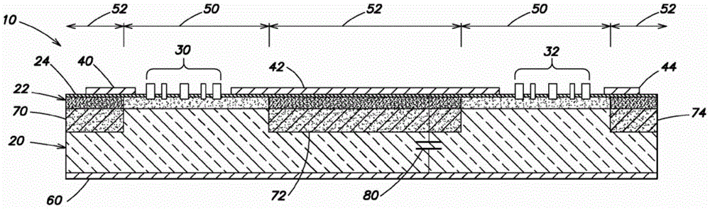
A simplified schematic cross-sectional view of a semiconductor structure 10 according to an embodiment is shown in fig. 1. Semiconductor structure 10 includes a substrate, such as a silicon substrate 20, a layer of group III-nitride material, such as a gallium nitride layer 22, a passivation/encapsulation layer 24, one or more devices 30 and 32 (shown schematically in fig. 1), and one or more interconnects 40, 42, and 44. Devices 30 and 32 are located in one or more device regions 50 of silicon substrate 20, and interconnects 40, 42, and 44 are located in one or more interconnect regions 52 of silicon substrate 20. Devices 30 and 32 may include, for example, gallium nitride transistors, and interconnects 40, 42, and 44 may include, for example, one or more metal interconnect lines and/or one or more metal bond pads. The interconnects may interconnect devices on the substrate and/or may provide external connections. The metal layer 60 may be formed on the backside of the silicon substrate 20, and the metal layer 60 may serve as a ground plate.
As further shown in fig. 1, semiconductor structure 10 includes low dielectric constant material regions 70, 72, and 74 formed in silicon substrate 20. In the low dielectric constant material regions 70, 72, and 74, silicon of the silicon substrate 20 is replaced with a material having a dielectric constant lower than that of the silicon substrate. In the embodiment of fig. 1, the low dielectric constant material is silicon dioxide, and regions 70, 72, and 74 will be referred to as silicon dioxide regions 70, 72, and 74. The dielectric constant of silicon is 11.65 and the dielectric constant of silicon dioxide is 3.9. Silicon dioxide regions 70, 72, and 74 underlie interconnects 40, 42, and 44, respectively. Thus, silicon dioxide regions 70, 72, and 74 are located between the respective interconnects and metal layer 60 on the backside of silicon substrate 20.
Parasitic capacitance
The parasitic capacitance between interconnect 42 and metal layer 60 is represented in fig. 1 as parasitic capacitor 80. Interconnect 42 forms a first plate of a parasitic capacitor, metal layer 60 forms a second plate of the parasitic capacitor, and the layer of structure between interconnect 42 and metal layer 60 forms the dielectric of the parasitic capacitor. A parasitic capacitor is also formed between each of the interconnects 40 and 44 and the metal layer 60. The parasitic capacitor degrades the performance of the semiconductor structure. It should be understood that parasitic capacitance is a distributed effect over the area of interconnects 40, 42, 44 and metal layer 60. As is known, the capacitance of a parallel plate capacitor is proportional to the dielectric constant of the dielectric material between the parallel plates. Thus, parasitic capacitance can be reduced by disposing a dielectric material having a dielectric constant lower than that of silicon between the plates of the capacitor.
In some embodiments, the semiconductor structure does not include a metal layer on the back surface of the substrate. However, in such embodiments, the semiconductor structure may be grounded in use, and there is a parasitic capacitance between the interconnect and ground, whether or not the semiconductor structure includes a metal layer on its back surface.
Referring to fig. 1, the region between interconnect 42 and metal layer 60 is partially filled with silicon dioxide region 72. By providing silicon dioxide region 72 between interconnect 42 and metal layer 60, the dielectric constant of the dielectric material of the parasitic capacitor is reduced compared to silicon as the dielectric material, thereby reducing the parasitic capacitance. In other embodiments, the low dielectric constant material may be a material having a low dielectric constant and that can withstand the epitaxial growth temperatures of subsequently formed group III nitride materials.
Silicon dioxide regions 70, 72, and 74 may underlie some or all of the interconnects on semiconductor structure 10. Furthermore, each of the silicon dioxide regions 70, 72, and 74 should actually be as much as possible below the respective interconnect to achieve the greatest reduction in parasitic capacitance.
Substrate
As described above, the substrate may comprise silicon (i.e., a substrate comprising any form of elemental silicon). Some embodiments relate to a substrate at least a portion of which is made of silicon. Some embodiments relate to a substrate at least a portion of which (or all of which) is made of bulk silicon. As used herein, bulk silicon refers to any form of doped or undoped elemental Si. A substrate comprising bulk silicon may comprise, for example, at least one layer of doped or undoped silicon, as opposed to silicon oxide, silicon carbide, silicon nitride, and the like. Examples of silicon-containing substrates that may be used in various embodiments include, but are not limited to, bulk silicon wafers, silicon-on-insulator substrates, and substrates made of silicon alloys (e.g., silicon germanium and silicon carbide substrates). In some embodiments, the substrate comprises a silicon substrate. As used herein, a silicon substrate refers to any substrate including a silicon surface. Examples of suitable silicon substrates include substrates consisting entirely of silicon (e.g., bulk silicon wafers), silicon-on-insulator (SOI) substrates, and silicon-on-sapphire (SOS) substrates. Suitable silicon substrates also include composite substrates having a silicon wafer bonded to another material, such as other crystalline forms of diamond or carbon, aluminum nitride (AlN), silicon carbide (SiC), or other crystalline or polycrystalline materials. Silicon substrates having different crystal orientations may be used, although in some, but not all embodiments, single crystal silicon substrates may be preferred. In some embodiments, a silicon (111) substrate is used. In some embodiments, a silicon (100) or (110) substrate is used. As used herein, a silicon carbide substrate refers to any substrate that includes a silicon carbide surface. Examples of suitable silicon carbide substrates include substrates consisting entirely of silicon carbide (e.g., bulk silicon carbide wafers), silicon carbide composite wafers (e.g., wafers comprising a silicon carbide layer and a second layer of non-silicon carbide material), and the like.
In some embodiments, the substrate can have any of a variety of suitable thicknesses. According to some embodiments, the final thickness of the substrate after processing and any wafer thinning is less than 150 microns. According to some embodiments, the substrate has a final thickness of less than 100 microns, less than 50 microns, or less. According to some embodiments, the final thickness of the substrate may be selected based on, for example, the final device and heteroepitaxial specifications (e.g., wafer warpage and bow) required for successful high-yield semiconductor fabrication. In some embodiments, the thickness of the substrate may be a semi-spec thickness (semi-spec thickness) typical of the wafer diameter used in large-scale wafer silicon manufacturing.
Group III nitride materials
As used herein, the term "group III nitride material" refers to any group III element nitride compound. Non-limiting examples of group III nitride materials include Boron Nitride (BN), aluminum nitride (AlN), gallium nitride (GaN), indium nitride (InN), and thallium nitride (TIN), as well as any alloy containing a group III element and a group V element (e.g., Al)xGa(1-x)N、AlxInyGa(1-x-y)N、InyGa(1-y)N、AlxIn(1-x)N、GaAsaPbN(1-a-b)、AlxInyGa(1-x-y)AsaPbN(1-a-b)Etc.). Typically, when present, arsenic and/or phosphorus are at low concentrations (e.g., less than 5 weight percent). The group III nitride material may be n-type or p-type doped, or may be intrinsic. The group III nitride material may have any polarity including, but not limited to, Ga-polar, N-polar, semi-polar, or non-polar crystal orientations. Group IIIThe nitride material may also include wurtzite, zincite, or mixed polytypes, and may include single crystal, polycrystalline, or amorphous structures.
In some embodiments, the group III-nitride material region comprises a gallium nitride material. As used herein, the phrase "gallium nitride material" refers to gallium nitride (GaN) and any alloys thereof, such as aluminum gallium nitride (Al)xGa(1-x)N), indium gallium nitride (In)yGa(1-y)N), aluminum indium gallium nitride (Al)xInyGa(1-x-y)N), arsenic phosphorus nitride (GaAs)aPbN(1-a-b)) AlInGaAsP nitride (Al)xInyGa(1-x-y)AsaPbN(1-a-b)) And the like. In certain embodiments, the group III nitride material region comprises GaN. According to some embodiments, the III-nitride material region is an epitaxial III-nitride material region. In certain embodiments, the group III nitride material region comprises a heterojunction two-dimensional electron gas (2DEG) region or a two-dimensional hole gas (2 DHG). In some embodiments, the group III nitride material region includes a doped homojunction and/or a doped heterojunction.
Process for producing a metal oxide
A process for fabricating a semiconductor structure according to an embodiment is described with reference to fig. 2 to 10, steps of which are shown in fig. 2 to 10. It will be understood that one or more of the steps described herein may be omitted, and that other steps may be included in the overall process. In some embodiments, the steps of the process may be performed in an order different than that described herein.
Referring to fig. 2, the process starts with a silicon substrate 20. The silicon substrate 20 may be p-type or n-type and may have any suitable conductivity. The silicon substrate 20 may have a thickness in the range of 500 μm to 1000 μm, but this is not limitative. In one example, the silicon substrate may be 625 μm, 100mm diameter 0.02 Ω -cm boron doped silicon. The silicon substrate 20 is referred to as having a front side 28 and a back side 26. Other examples of substrates include, but are not limited to, 675 μm, 0.02 Ω -cm silicon with a diameter of 150 mm; 725 μm, 0.02. omega. -cm diameter silicon; and 775 μm, 0.02. omega. -cm silicon with a diameter of 300 mm.
Referring to fig. 3, a mask layer such as a silicon
nitride mask layer 110 is formed on the top surface of the
silicon substrate 20. The silicon
nitride mask layer 110 may be formed by Low Pressure Chemical Vapor Deposition (LPCVD) and may have
To
But this is not limiting. Other suitable mask layers include Plasma Enhanced (PECVD) silicon nitride(s) ((s))>550C deposition temperature/zero trapped hydrogen), sputtered silicon nitride, Atomic Layer Deposition (ALD) of silicon nitride, or layered combinations of these films with or without an added LPCVD silicon nitride layer. Any non-oxidizing material that is attached to a silicon substrate, that can be patterned by standard photolithographic processes, and that can withstand silicon oxidation temperatures can be used.
Referring to fig. 4, the silicon nitride mask layer 110 is patterned using conventional patterning techniques. For example, a mask defining a region of the silicon nitride layer 110 to be removed is placed over the silicon nitride layer 110, and an etching step is performed. The patterned mask is formed by a typical photolithography process that employs a photosensitive organic polymer (photoresist) temporarily applied to the surface of a silicon nitride mask layer. The photoresist pattern is transferred to the silicon nitride mask layer by standard dry etch plasma, RIE (reactive ion etching) or ICP (inductively coupled plasma) techniques. The temporary patterned photoresist is then removed by a dry or wet chemical process.
After patterning, the silicon nitride layer 110 remains in the device region 50 and is removed in the interconnect region 52 to expose the silicon substrate 20. It will be understood that device regions 50 do not necessarily match the regions occupied by devices, and interconnect regions 52 do not necessarily match the regions occupied by interconnects. In contrast, interconnect region 52 defines a region in which silicon substrate 20 is at least partially replaced with a low dielectric constant material, while device region 50 defines a region in which silicon substrate 20 is not replaced with a low dielectric constant material. The interconnect may extend from the interconnect region to the device region for connection to the device.
Referring to fig. 5, an etching step is performed on the substrate 20 partially covered by the patterned silicon nitride layer 110. The etching process removes the portion of the silicon substrate not covered by the silicon nitride layer 110. In particular, the etching process removes silicon of substrate 20 in interconnect region 52 to form trenches 130, 132, and 134. Trenches 130, 132, and 134 are formed to have a controlled depth 136 based on the desired thickness of the subsequently formed oxide regions. The depth 136 of trenches 130, 132, and 134 may be defined as the depth from the top surface of silicon substrate 20 in device region 50 to the surface 138 of silicon substrate 20 in trenches 130, 132, and 134 after the trenches are formed and before oxidation. The depth of the trench depends on the thickness of the substrate 20 in the final structure and may be 0.5% to 10% of the thickness of the substrate. In one example, the depth 136 of the trenches 130, 132, and 134 can be about 5 microns to form oxide regions having a depth of about 10 microns. It will be understood that this example is not limiting. Device region 50 under portions 120 and 122 of silicon nitride layer 110 is not affected by the etching process.
Referring to fig. 6, a thermal oxidation step is performed on substrate 20 masked by portions 120 and 122 of silicon nitride layer 110. This thermal oxidation step oxidizes the silicon substrate 20 in trenches 130, 132 and 134 while leaving device region 50, which is masked by portions 120 and 122 of silicon nitride layer 110, unaffected. In particular, the silicon in trenches 130, 132, and 134 is oxidized to form silicon dioxide. The thermal oxidation step is continued until silicon dioxide fills trenches 130, 132, and 134 to form silicon dioxide regions 70, 72, and 74, respectively. A thermal oxidation step is performed until the top surfaces of silicon dioxide regions 70, 72, and 74 are substantially coplanar with the top surface of silicon substrate 20 in device region 50. The thermal oxidation step may be part of a LOCOS process.
After thermal oxidation of the silicon, silicon dioxide regions extend above and below the trench surface 138 after trench formation and before oxidation. In particular, prior to oxidation, approximately 54% of the silicon dioxide thickness (represented as thickness 140) is above trench surface 138, and prior to oxidation, approximately 46% of the silicon dioxide thickness (represented as thickness 142) is below trench surface 138. By appropriate selection of the trench depth and thermal oxidation parameters, silicon dioxide regions 70, 72 and 74 may be formed that are almost twice the trench depth and are coplanar or nearly coplanar with the top surface of silicon substrate 20 in device region 50.
For atmospheric pressure, typical oxidation temperatures range from 1000 degrees Celsius to 1200 degrees Celsius. The oxidizing species are formed by combining hydrogen and oxygen to create a saturated steam environment. Time is used as a variable parameter to increase the desired silica thickness. The use of a HiPOX (high pressure oxidation) system can reduce both the temperature and time required to produce the desired silica thickness. In this HiPOX process, hydrogen and oxygen are recombined to produce steam, but the pressure is increased significantly, typically in the range of 10 to 25 times atmospheric pressure.
Referring to fig. 7, the silicon nitride layer 110 is stripped from the surface of the silicon substrate 20 by etching. The silicon nitride mask layer is removed via phosphoric acid at an elevated temperature, typically in the range between 120 degrees celsius and 200 degrees celsius. Alternatively, the silicon nitride film may be removed by chemical mechanical polishing the silicon surface. After removal of the silicon nitride layer 110, the surface of the silicon substrate 20 is exposed in the device region 50, while the silicon dioxide is exposed in the interconnect region 52. Preferably, the planarity of the surface is maintained at the boundary between the silicon in the device region 50 and the silicon dioxide in the interconnect region 52. In some embodiments, the surface of the silicon substrate may be polished to ensure a flat surface.
Referring to fig. 8, an epitaxial growth step is performed. In particular, a gallium nitride layer 22 or other group III nitride material layer is formed on the top surface of the silicon substrate 20 by epitaxial growth. The thickness of the gallium nitride layer 22 may be in the range of 0.8 μm to 6 μm, but this is not limiting. As shown in fig. 8, gallium nitride layer 22 may include single crystal gallium nitride 152 in device region 50 and may include polycrystalline gallium nitride 154 in interconnect region 52. Monocrystalline gallium nitride 152 is formed on silicon substrate 20 and polycrystalline gallium nitride 154 is formed on silicon dioxide regions 70, 72, and 74. A passivation/encapsulation layer 24 is then formed on the gallium nitride layer 22. In some embodiments, polycrystalline gallium nitride 154 in interconnect region 52 may be removed prior to fabricating interconnects 40, 42, and 44.
Referring to fig. 9, devices 30 and 32 are fabricated in device region 50, and interconnects 40, 42, and 44 are fabricated in interconnect region 52. Devices 30 and 32 are formed by etching openings in passivation/encapsulation layer 24 and forming, for example, source, gate and drain structures. Interconnects 40, 42, 44 are deposited on the top surface of passivation/encapsulation layer 24 and are electrically connected to one or more of devices 30 and 32. The connection of devices 30 and 32 is not shown and may occur out of the plane of the drawing.
One or more devices, such as gallium nitride transistors, may be formed in each device region 50. Further, one or more interconnects may be formed in each interconnect region 52. The interconnects may be interconnect lines for interconnecting devices and/or bond pads, bond pads for bonding of external connection lines, or both. The interconnect lines and the bond pads may be fabricated as at least one patterned metal layer. Active devices 30 and 32 and interconnects 40, 42, and 44 may be fabricated according to known techniques.
Referring to fig. 10, the thickness of the silicon substrate 20 is reduced by thinning the backside. GaN on silicon wafers is mounted with the front side down on a carrier substrate using wax or other organic polymer that provides temporary bonding to the carrier wafer, which provides a rigid handle that supports the active device wafer when the thinning process is performed. The carrier material may be sapphire, glass, silicon or silicon carbide. The actual thinning is achieved by removing a significant amount of unwanted silicon using a typical semiconductor diamond wheel grinding process. Then, the grinding of the silicon is followed by chemical mechanical polishing with colloidal silicon dioxide to remove the remaining grinding damage. The thickness of the substrate 20 may be reduced to a final thickness in the range of 50 μm to 100 μm, but this is not limitative. After thinning the silicon substrate 20, a metal layer 60 is formed on the back surface of the thinned substrate. The metal layer 60 may have a thickness in the range of 1 μm to 6 μm, and may serve as a ground plate of the semiconductor device.
In the completed semiconductor structure 10, each of the interconnects 40, 42, and 44 may be separated from the metal layer 60 in the interconnect region 52 by the polycrystalline gallium nitride 154, the silicon dioxide regions 70, 72, and 74, and the silicon substrate 20. Because silicon substrate 20 is partially replaced in interconnect region 52 by silicon dioxide having a lower dielectric constant than silicon, the overall dielectric constant of the material between each of interconnects 40, 42, and 44 and metal layer 60 is reduced. The reduction in dielectric constant in turn reduces the parasitic capacitance between interconnects 40, 42 and 44 and metal layer 60, thereby improving performance, particularly at high frequencies. It will be appreciated that the beneficial effects of silicon dioxide regions 70, 72, and 74 may be increased by increasing the thickness of these regions relative to the overall thickness of silicon substrate 20 and/or by increasing the area of silicon dioxide regions 70, 72, and 74 under interconnects 40, 42, and 44.
In the embodiments described herein, the portion of the silicon substrate 20 underlying the interconnect is replaced by silicon dioxide, which has a lower dielectric constant than silicon. In other embodiments, the silicon in the interconnect region 52 may be replaced with other materials that have a lower dielectric constant than silicon and may withstand the epitaxial growth temperatures of subsequently formed group III nitride materials to achieve a reduction in parasitic capacitance. In further embodiments, substrate 20 may be a different material than silicon, such as silicon carbide.
In further embodiments, the devices in device regions 50 may be any suitable active and/or passive circuit components, and each device region 50 may include one or more circuit components of the same or different types. In some embodiments, the semiconductor structure includes a single device region 50 and a single interconnect region 52. The number of device regions 50 and the number of interconnect regions 52 are not limiting.
The semiconductor structure has been described as including a layer of group III nitride material. In some embodiments, the semiconductor structure includes one or more layers in addition to the layer of group III nitride material, including but not limited to a diffusion barrier layer, a nucleation layer, and/or a buffer layer.
Device using semiconductor structure
The semiconductor structures described herein may form the basis of various semiconductor devices, according to some embodiments. Suitable devices include, but are not limited to, discrete devices such as transistors (e.g., Field Effect Transistors (FETs); enhancement or depletion mode), schottky diodes, and light emitting devices including Light Emitting Diodes (LEDs) and laser diodes. Likewise, suitable devices also include integrated circuits (e.g., Monolithic Microwave Integrated Circuits (MMICs), combinations of two or more discrete devices, such as for assembly of front-end modules (FEMs)). According to some, but not necessarily all, embodiments, it is particularly advantageous to use these structures in devices that operate at high frequencies (e.g., 100MHz or higher for some power management applications and 1GHz or higher for some RF applications). Non-limiting examples of the use of group III nitride devices operating at higher frequencies include power management discrete devices and integrated circuits (e.g., buck converters, boost converters, half bridges, H bridges, full bridges, three phase bridges, and multiphase bridges) for switching, rectifying, monitoring, or controlling power from a power source to a load. Other non-limiting examples of RF applications include discrete and integrated devices for transmit and receive functions related to wireless and wired communication, RF energy, RF plasma lighting, wireless charging, RF induction, and microwave heating, RF spark plugs, ISM, medical devices, RADAR, and electronic warfare and countermeasure devices. In some embodiments, there may be an integrated circuit and/or multiple dies on the chip that incorporate both RF devices and switching devices for monitoring, switching, or controlling the delivery of power from the power source to the load.
In accordance with certain embodiments, the device has an active region that is typically formed at least partially in the group III-nitride material region (e.g., in one or more layers of the group III-nitride material device region, such as one or more layers of gallium nitride material). According to some embodiments, the device includes various other functional layers and/or features (e.g., electrodes, dielectric regions, field plate layers, etc.).
According to some embodiments, the semiconductor structure includes a transistor (e.g., a Field Effect Transistor (FET)). According to some embodiments, the transistor may include a source electrode and a drain electrode. The source and drain electrodes may be electrically isolated from each other. For example, in some embodiments, the source and drain electrodes are spatially separated by a dielectric material. In some embodiments, the transistor further comprises a gate electrode. The gate electrode may be a schottky gate electrode or an insulated gate electrode. According to some embodiments, during use, application of a voltage across the gate electrode may generate and/or alter an electric field at least partially between the source electrode and the drain electrode such that electrons are transferred from the source electrode to the drain electrode. Suitable transistors (e.g., FETs) that may be used in conjunction with certain embodiments described herein include depletion-mode (normally-on) transistors and enhancement-mode (normally-off) transistors.
While several embodiments of the invention have been described and illustrated herein, those of ordinary skill in the art will readily envision a variety of other means and/or structures for performing the function and/or obtaining the results and/or one or more of the advantages described herein, and each of such variations and/or modifications is deemed to be within the scope of the present technology. More generally, those skilled in the art will readily appreciate that all parameters, dimensions, materials, and configurations described herein are meant to be exemplary and that the actual parameters, dimensions, materials, and/or configurations will depend upon the specific application or applications for which the teachings of the present technology is used. Those skilled in the art will understand (or be able to ascertain using no more than routine experimentation) many equivalents to the specific embodiments of the techniques described herein. It is, therefore, to be understood that the foregoing embodiments are presented by way of example only and that, within the scope of the appended claims and equivalents thereto, the technology may be practiced otherwise than as specifically described and claimed. The present technology is directed to each individual feature, system, article, material, and/or method described herein. In addition, any combination of two or more such features, systems, articles, materials and/or methods, if such features, systems, articles, materials and/or methods are not mutually inconsistent, is included within the scope of the present technology.
As defined and used herein, all definitions should be understood to control dictionary definitions, definitions in documents incorporated by reference, and/or ordinary meanings of the defined terms.
As used herein in the specification and in the claims, the indefinite articles "a" and "an" should be understood to mean "at least one" unless clearly indicated to the contrary.
As used herein in the specification and claims, the phrase "and/or" should be understood to mean "either or both" of the elements so connected, i.e., elements that are present in connection in some cases and elements that are present in isolation in other cases. In addition to elements specifically identified by the "and/or" clause, other elements may optionally be present, whether related or unrelated to those elements specifically identified unless clearly indicated to the contrary. Thus, as a non-limiting example, when used in conjunction with open-ended language (e.g., "including"), references to "a and/or B" may refer in one embodiment to a alone (optionally including elements other than B); in another embodiment, only B (optionally including elements other than a); in yet another embodiment, to a and B (optionally including other elements), and the like.
As used herein in the specification and claims, "or" should be understood to have the same meaning as "and/or" as defined above. For example, when separating items in a list, "or" and/or "should be interpreted as inclusive, i.e., including at least one of a plurality of elements or lists of elements but also including more than one of the plurality of elements or lists of elements, and optionally including other unlisted items. Only terms explicitly indicated to the contrary, such as "only one" or "exactly one," or "consisting of," when used in a claim, shall mean including a plurality of elements or exactly one of a list of elements. In general, the term "or" as used herein, when preceded by an exclusive term such as "any," "one," "only one," or "exactly one," should only be construed to indicate an exclusive alternative (i.e., "one or the other but not both"). "consisting essentially of, when used in the claims, shall have its ordinary meaning as used in the patent law.
As used in the specification and claims, the phrase "at least one," when referring to a list of one or more elements, should be understood to mean at least one element selected from any one or more of the elements in the list of elements, without necessarily including at least one of each or every element specifically enumerated in the list of elements, and without excluding any combinations of elements in the list of elements. The definition also allows that elements may optionally be present other than the elements specifically identified in the list of elements to which the phrase "at least one" refers, whether related or unrelated to those elements specifically identified. Thus, as a non-limiting example, "at least one of a and B" (or, equivalently, "at least one of a or B," or, equivalently, "at least one of a and/or B") can refer in one embodiment to at least one a, optionally including more than one a, with no B present (and optionally including elements other than B); in another embodiment, to at least one B, optionally including more than one B, no a is present (and optionally including elements other than a); in yet another embodiment, to at least one, optionally including more than one, a, and at least one, optionally including more than one, B (and optionally including other elements); and the like.
In the claims, as well as in the specification above, all conjunctions such as "comprising," "including," "carrying," "having," "containing," "involving," "holding," and the like are to be understood as open-ended, i.e., to mean including but not limited to. Only the conjunctions "consisting of … …" and "consisting essentially of … …" may be respectively a closed or semi-closed conjunctions as explained in detail in the us patent office patent examination program manual (section 2111.03).
Having described in detail several embodiments of the technology described herein, various modifications and improvements will readily occur to those skilled in the art. Such modifications and improvements are intended to be within the spirit and scope of this disclosure. Accordingly, the foregoing description is by way of example only and is not intended as limiting. The technology is limited only as defined in the following claims and the equivalents thereto.