CN112216612A - Thin film transistor substrate, display device including the same, and methods of manufacturing the same - Google Patents
Thin film transistor substrate, display device including the same, and methods of manufacturing the same Download PDFInfo
- Publication number
- CN112216612A CN112216612A CN202010655636.5A CN202010655636A CN112216612A CN 112216612 A CN112216612 A CN 112216612A CN 202010655636 A CN202010655636 A CN 202010655636A CN 112216612 A CN112216612 A CN 112216612A
- Authority
- CN
- China
- Prior art keywords
- amorphous silicon
- silicon layer
- substrate
- layer
- thin film
- Prior art date
- Legal status (The legal status is an assumption and is not a legal conclusion. Google has not performed a legal analysis and makes no representation as to the accuracy of the status listed.)
- Granted
Links
Images


Classifications
-
- H—ELECTRICITY
- H10—SEMICONDUCTOR DEVICES; ELECTRIC SOLID-STATE DEVICES NOT OTHERWISE PROVIDED FOR
- H10D—INORGANIC ELECTRIC SEMICONDUCTOR DEVICES
- H10D30/00—Field-effect transistors [FET]
- H10D30/60—Insulated-gate field-effect transistors [IGFET]
- H10D30/67—Thin-film transistors [TFT]
- H10D30/674—Thin-film transistors [TFT] characterised by the active materials
- H10D30/6741—Group IV materials, e.g. germanium or silicon carbide
- H10D30/6743—Silicon
- H10D30/6745—Polycrystalline or microcrystalline silicon
-
- H—ELECTRICITY
- H10—SEMICONDUCTOR DEVICES; ELECTRIC SOLID-STATE DEVICES NOT OTHERWISE PROVIDED FOR
- H10P—GENERIC PROCESSES OR APPARATUS FOR THE MANUFACTURE OR TREATMENT OF DEVICES COVERED BY CLASS H10
- H10P14/00—Formation of materials, e.g. in the shape of layers or pillars
- H10P14/20—Formation of materials, e.g. in the shape of layers or pillars of semiconductor materials
- H10P14/34—Deposited materials, e.g. layers
- H10P14/3402—Deposited materials, e.g. layers characterised by the chemical composition
- H10P14/3404—Deposited materials, e.g. layers characterised by the chemical composition being Group IVA materials
- H10P14/3411—Silicon, silicon germanium or germanium
-
- H—ELECTRICITY
- H10—SEMICONDUCTOR DEVICES; ELECTRIC SOLID-STATE DEVICES NOT OTHERWISE PROVIDED FOR
- H10D—INORGANIC ELECTRIC SEMICONDUCTOR DEVICES
- H10D30/00—Field-effect transistors [FET]
- H10D30/60—Insulated-gate field-effect transistors [IGFET]
- H10D30/67—Thin-film transistors [TFT]
- H10D30/674—Thin-film transistors [TFT] characterised by the active materials
- H10D30/6741—Group IV materials, e.g. germanium or silicon carbide
- H10D30/6743—Silicon
-
- H—ELECTRICITY
- H10—SEMICONDUCTOR DEVICES; ELECTRIC SOLID-STATE DEVICES NOT OTHERWISE PROVIDED FOR
- H10D—INORGANIC ELECTRIC SEMICONDUCTOR DEVICES
- H10D30/00—Field-effect transistors [FET]
- H10D30/01—Manufacture or treatment
- H10D30/021—Manufacture or treatment of FETs having insulated gates [IGFET]
- H10D30/024—Manufacture or treatment of FETs having insulated gates [IGFET] of fin field-effect transistors [FinFET]
-
- H—ELECTRICITY
- H10—SEMICONDUCTOR DEVICES; ELECTRIC SOLID-STATE DEVICES NOT OTHERWISE PROVIDED FOR
- H10D—INORGANIC ELECTRIC SEMICONDUCTOR DEVICES
- H10D30/00—Field-effect transistors [FET]
- H10D30/01—Manufacture or treatment
- H10D30/021—Manufacture or treatment of FETs having insulated gates [IGFET]
- H10D30/031—Manufacture or treatment of FETs having insulated gates [IGFET] of thin-film transistors [TFT]
- H10D30/0312—Manufacture or treatment of FETs having insulated gates [IGFET] of thin-film transistors [TFT] characterised by the gate electrodes
- H10D30/0314—Manufacture or treatment of FETs having insulated gates [IGFET] of thin-film transistors [TFT] characterised by the gate electrodes of lateral top-gate TFTs comprising only a single gate
-
- H—ELECTRICITY
- H10—SEMICONDUCTOR DEVICES; ELECTRIC SOLID-STATE DEVICES NOT OTHERWISE PROVIDED FOR
- H10D—INORGANIC ELECTRIC SEMICONDUCTOR DEVICES
- H10D30/00—Field-effect transistors [FET]
- H10D30/01—Manufacture or treatment
- H10D30/021—Manufacture or treatment of FETs having insulated gates [IGFET]
- H10D30/031—Manufacture or treatment of FETs having insulated gates [IGFET] of thin-film transistors [TFT]
- H10D30/0321—Manufacture or treatment of FETs having insulated gates [IGFET] of thin-film transistors [TFT] comprising silicon, e.g. amorphous silicon or polysilicon
-
- H—ELECTRICITY
- H10—SEMICONDUCTOR DEVICES; ELECTRIC SOLID-STATE DEVICES NOT OTHERWISE PROVIDED FOR
- H10D—INORGANIC ELECTRIC SEMICONDUCTOR DEVICES
- H10D30/00—Field-effect transistors [FET]
- H10D30/60—Insulated-gate field-effect transistors [IGFET]
- H10D30/67—Thin-film transistors [TFT]
- H10D30/6704—Thin-film transistors [TFT] having supplementary regions or layers in the thin films or in the insulated bulk substrates for controlling properties of the device
- H10D30/6713—Thin-film transistors [TFT] having supplementary regions or layers in the thin films or in the insulated bulk substrates for controlling properties of the device characterised by the properties of the source or drain regions, e.g. compositions or sectional shapes
-
- H—ELECTRICITY
- H10—SEMICONDUCTOR DEVICES; ELECTRIC SOLID-STATE DEVICES NOT OTHERWISE PROVIDED FOR
- H10D—INORGANIC ELECTRIC SEMICONDUCTOR DEVICES
- H10D30/00—Field-effect transistors [FET]
- H10D30/60—Insulated-gate field-effect transistors [IGFET]
- H10D30/67—Thin-film transistors [TFT]
- H10D30/6729—Thin-film transistors [TFT] characterised by the electrodes
- H10D30/673—Thin-film transistors [TFT] characterised by the electrodes characterised by the shapes, relative sizes or dispositions of the gate electrodes
- H10D30/6731—Top-gate only TFTs
-
- H—ELECTRICITY
- H10—SEMICONDUCTOR DEVICES; ELECTRIC SOLID-STATE DEVICES NOT OTHERWISE PROVIDED FOR
- H10D—INORGANIC ELECTRIC SEMICONDUCTOR DEVICES
- H10D30/00—Field-effect transistors [FET]
- H10D30/60—Insulated-gate field-effect transistors [IGFET]
- H10D30/67—Thin-film transistors [TFT]
- H10D30/674—Thin-film transistors [TFT] characterised by the active materials
- H10D30/6755—Oxide semiconductors, e.g. zinc oxide, copper aluminium oxide or cadmium stannate
-
- H—ELECTRICITY
- H10—SEMICONDUCTOR DEVICES; ELECTRIC SOLID-STATE DEVICES NOT OTHERWISE PROVIDED FOR
- H10D—INORGANIC ELECTRIC SEMICONDUCTOR DEVICES
- H10D30/00—Field-effect transistors [FET]
- H10D30/60—Insulated-gate field-effect transistors [IGFET]
- H10D30/67—Thin-film transistors [TFT]
- H10D30/6757—Thin-film transistors [TFT] characterised by the structure of the channel, e.g. transverse or longitudinal shape or doping profile
-
- H—ELECTRICITY
- H10—SEMICONDUCTOR DEVICES; ELECTRIC SOLID-STATE DEVICES NOT OTHERWISE PROVIDED FOR
- H10D—INORGANIC ELECTRIC SEMICONDUCTOR DEVICES
- H10D86/00—Integrated devices formed in or on insulating or conducting substrates, e.g. formed in silicon-on-insulator [SOI] substrates or on stainless steel or glass substrates
- H10D86/01—Manufacture or treatment
- H10D86/021—Manufacture or treatment of multiple TFTs
- H10D86/0221—Manufacture or treatment of multiple TFTs comprising manufacture, treatment or patterning of TFT semiconductor bodies
- H10D86/0223—Manufacture or treatment of multiple TFTs comprising manufacture, treatment or patterning of TFT semiconductor bodies comprising crystallisation of amorphous, microcrystalline or polycrystalline semiconductor materials
-
- H—ELECTRICITY
- H10—SEMICONDUCTOR DEVICES; ELECTRIC SOLID-STATE DEVICES NOT OTHERWISE PROVIDED FOR
- H10D—INORGANIC ELECTRIC SEMICONDUCTOR DEVICES
- H10D86/00—Integrated devices formed in or on insulating or conducting substrates, e.g. formed in silicon-on-insulator [SOI] substrates or on stainless steel or glass substrates
- H10D86/40—Integrated devices formed in or on insulating or conducting substrates, e.g. formed in silicon-on-insulator [SOI] substrates or on stainless steel or glass substrates characterised by multiple TFTs
- H10D86/421—Integrated devices formed in or on insulating or conducting substrates, e.g. formed in silicon-on-insulator [SOI] substrates or on stainless steel or glass substrates characterised by multiple TFTs having a particular composition, shape or crystalline structure of the active layer
-
- H—ELECTRICITY
- H10—SEMICONDUCTOR DEVICES; ELECTRIC SOLID-STATE DEVICES NOT OTHERWISE PROVIDED FOR
- H10D—INORGANIC ELECTRIC SEMICONDUCTOR DEVICES
- H10D86/00—Integrated devices formed in or on insulating or conducting substrates, e.g. formed in silicon-on-insulator [SOI] substrates or on stainless steel or glass substrates
- H10D86/40—Integrated devices formed in or on insulating or conducting substrates, e.g. formed in silicon-on-insulator [SOI] substrates or on stainless steel or glass substrates characterised by multiple TFTs
- H10D86/60—Integrated devices formed in or on insulating or conducting substrates, e.g. formed in silicon-on-insulator [SOI] substrates or on stainless steel or glass substrates characterised by multiple TFTs wherein the TFTs are in active matrices
-
- H—ELECTRICITY
- H10—SEMICONDUCTOR DEVICES; ELECTRIC SOLID-STATE DEVICES NOT OTHERWISE PROVIDED FOR
- H10K—ORGANIC ELECTRIC SOLID-STATE DEVICES
- H10K59/00—Integrated devices, or assemblies of multiple devices, comprising at least one organic light-emitting element covered by group H10K50/00
- H10K59/10—OLED displays
- H10K59/12—Active-matrix OLED [AMOLED] displays
- H10K59/121—Active-matrix OLED [AMOLED] displays characterised by the geometry or disposition of pixel elements
- H10K59/1213—Active-matrix OLED [AMOLED] displays characterised by the geometry or disposition of pixel elements the pixel elements being TFTs
-
- H—ELECTRICITY
- H10—SEMICONDUCTOR DEVICES; ELECTRIC SOLID-STATE DEVICES NOT OTHERWISE PROVIDED FOR
- H10K—ORGANIC ELECTRIC SOLID-STATE DEVICES
- H10K71/00—Manufacture or treatment specially adapted for the organic devices covered by this subclass
-
- H—ELECTRICITY
- H10—SEMICONDUCTOR DEVICES; ELECTRIC SOLID-STATE DEVICES NOT OTHERWISE PROVIDED FOR
- H10K—ORGANIC ELECTRIC SOLID-STATE DEVICES
- H10K71/00—Manufacture or treatment specially adapted for the organic devices covered by this subclass
- H10K71/40—Thermal treatment, e.g. annealing in the presence of a solvent vapour
-
- H—ELECTRICITY
- H10—SEMICONDUCTOR DEVICES; ELECTRIC SOLID-STATE DEVICES NOT OTHERWISE PROVIDED FOR
- H10P—GENERIC PROCESSES OR APPARATUS FOR THE MANUFACTURE OR TREATMENT OF DEVICES COVERED BY CLASS H10
- H10P14/00—Formation of materials, e.g. in the shape of layers or pillars
- H10P14/20—Formation of materials, e.g. in the shape of layers or pillars of semiconductor materials
- H10P14/32—Formation of materials, e.g. in the shape of layers or pillars of semiconductor materials characterised by intermediate layers between substrates and deposited layers
- H10P14/3202—Materials thereof
- H10P14/3238—Materials thereof being insulating materials
-
- H—ELECTRICITY
- H10—SEMICONDUCTOR DEVICES; ELECTRIC SOLID-STATE DEVICES NOT OTHERWISE PROVIDED FOR
- H10P—GENERIC PROCESSES OR APPARATUS FOR THE MANUFACTURE OR TREATMENT OF DEVICES COVERED BY CLASS H10
- H10P14/00—Formation of materials, e.g. in the shape of layers or pillars
- H10P14/20—Formation of materials, e.g. in the shape of layers or pillars of semiconductor materials
- H10P14/34—Deposited materials, e.g. layers
- H10P14/3451—Structure
- H10P14/3452—Microstructure
- H10P14/3454—Amorphous
-
- H—ELECTRICITY
- H10—SEMICONDUCTOR DEVICES; ELECTRIC SOLID-STATE DEVICES NOT OTHERWISE PROVIDED FOR
- H10P—GENERIC PROCESSES OR APPARATUS FOR THE MANUFACTURE OR TREATMENT OF DEVICES COVERED BY CLASS H10
- H10P14/00—Formation of materials, e.g. in the shape of layers or pillars
- H10P14/20—Formation of materials, e.g. in the shape of layers or pillars of semiconductor materials
- H10P14/36—Formation of materials, e.g. in the shape of layers or pillars of semiconductor materials characterised by treatments done before the formation of the materials
- H10P14/3602—In-situ cleaning
-
- H—ELECTRICITY
- H10—SEMICONDUCTOR DEVICES; ELECTRIC SOLID-STATE DEVICES NOT OTHERWISE PROVIDED FOR
- H10P—GENERIC PROCESSES OR APPARATUS FOR THE MANUFACTURE OR TREATMENT OF DEVICES COVERED BY CLASS H10
- H10P14/00—Formation of materials, e.g. in the shape of layers or pillars
- H10P14/20—Formation of materials, e.g. in the shape of layers or pillars of semiconductor materials
- H10P14/38—Formation of materials, e.g. in the shape of layers or pillars of semiconductor materials characterised by treatments done after the formation of the materials
- H10P14/3802—Crystallisation or recrystallisation of non-monocrystalline semiconductor materials, e.g. regrowth
- H10P14/3808—Crystallisation or recrystallisation of non-monocrystalline semiconductor materials, e.g. regrowth using laser beams
- H10P14/3816—Pulsed laser beam
-
- H—ELECTRICITY
- H10—SEMICONDUCTOR DEVICES; ELECTRIC SOLID-STATE DEVICES NOT OTHERWISE PROVIDED FOR
- H10P—GENERIC PROCESSES OR APPARATUS FOR THE MANUFACTURE OR TREATMENT OF DEVICES COVERED BY CLASS H10
- H10P70/00—Cleaning of wafers, substrates or parts of devices
- H10P70/10—Cleaning before device manufacture, i.e. Begin-Of-Line process
-
- H—ELECTRICITY
- H10—SEMICONDUCTOR DEVICES; ELECTRIC SOLID-STATE DEVICES NOT OTHERWISE PROVIDED FOR
- H10K—ORGANIC ELECTRIC SOLID-STATE DEVICES
- H10K59/00—Integrated devices, or assemblies of multiple devices, comprising at least one organic light-emitting element covered by group H10K50/00
- H10K59/10—OLED displays
- H10K59/12—Active-matrix OLED [AMOLED] displays
- H10K59/1201—Manufacture or treatment
Landscapes
- Engineering & Computer Science (AREA)
- Manufacturing & Machinery (AREA)
- Physics & Mathematics (AREA)
- Microelectronics & Electronic Packaging (AREA)
- Geometry (AREA)
- Electroluminescent Light Sources (AREA)
- Chemical & Material Sciences (AREA)
- Crystallography & Structural Chemistry (AREA)
- Recrystallisation Techniques (AREA)
- Devices For Indicating Variable Information By Combining Individual Elements (AREA)
- Thin Film Transistor (AREA)
- Optics & Photonics (AREA)
- Weting (AREA)
- Cleaning Or Drying Semiconductors (AREA)
Abstract
The present application relates to a thin film transistor substrate, a display device including the same, and methods of manufacturing the same, wherein the method of manufacturing the thin film transistor substrate includes: removing the oxide film on the surface of the amorphous silicon layer by performing surface cleaning; and forming an active layer by performing heat treatment on the amorphous silicon layer, wherein the amorphous silicon layer becomes crystalline silicon by the heat treatment.
Description
The present application claims priority and ownership gained from korean patent application No. 10-2019-0084545, filed on 12/7/2019, the contents of which are incorporated herein by reference in their entirety.
Technical Field
One or more embodiments relate to a thin film transistor substrate used in a display device or the like, and more particularly, to a thin film transistor substrate including an active layer having an improved structure, a display device including the thin film transistor substrate, and methods of manufacturing the thin film transistor substrate and the display device.
Background
In general, a display device, such as an organic light emitting display device, includes a thin film transistor for driving each pixel, and the thin film transistor includes an active layer. The active layer is typically formed in an amorphous state on the substrate and then crystallized by an appropriate heat treatment.
Disclosure of Invention
In the crystallization process for the active layer, protrusions protruding above the surface may be formed at boundaries between the crystallized grains. That is, during the heat treatment, as amorphous silicon is converted into crystalline silicon, crystalline grains collide while growing and form boundaries, and such projections may be formed on the surface at the grain boundaries where the collisions occur.
However, when the protrusion becomes too large, an electric field is concentrated at the tip thereof, and thus, a deviation in the electrical characteristics of the device may be increased, thereby causing undesirable instability. Further, the protrusions may be perceived by the user as a pattern, such as a moire pattern, as if there were undesirable spots on the screen. As a result, reliability of the product can be reduced.
In particular, an oxide film on the surface of an amorphous active layer before crystallization has been noted as a main element for increasing the size of the protrusion.
Accordingly, one or more embodiments include a thin film transistor substrate improved to solve excessive concentration of an electric field on a protrusion and screen quality failure due to visibility of a spot pattern by reducing the size of the protrusion formed at a grain boundary of an active layer; a display device including a thin film transistor substrate; and methods of manufacturing a thin film transistor substrate and a display device.
According to an embodiment, a method of manufacturing a thin film transistor substrate includes: providing an amorphous silicon layer over a substrate; removing the oxide film on the surface of the amorphous silicon layer by performing surface cleaning; and forming an active layer by performing a heat treatment on the amorphous silicon layer, wherein the amorphous silicon layer becomes a crystalline silicon layer by the heat treatment.
In an embodiment, removing the oxide film on the surface of the amorphous silicon layer by performing surface cleaning may include: the oxide film is removed by spraying a hydrogen fluoride solution onto the surface of the amorphous silicon layer.
In an embodiment, the hydrogen fluoride solution may include about 0.5 volume percent (vol%) hydrogen fluoride.
In an embodiment, removing the oxide film on the surface of the amorphous silicon layer by performing the surface cleaning may further include: a first rinsing cleaning is performed, including supplying hydrogen water to the surface of the amorphous silicon layer in a free-fall manner.
In an embodiment, removing the oxide film on the surface of the amorphous silicon layer by performing the surface cleaning may further include: a second rinsing cleaning is performed, which includes supplying hydrogen water to the surface of the amorphous silicon layer in a free-fall form while applying vibration to the hydrogen water with megasonic waves.
In an embodiment, forming the active layer may include: irradiating a laser beam onto an amorphous silicon layer disposed over a substrate, wherein the laser beam may have a long side and a short side in a first direction and a second direction perpendicular to each other, respectively; and moving the substrate by a predetermined pitch in a second direction parallel to the short sides.
In an embodiment, the laser beam may be repeatedly turned on and off every time the substrate moves by a predetermined pitch, wherein the predetermined pitch may be set to allow the laser beam to be turned on at least 7 times in the cell region of the amorphous silicon layer.
In an embodiment, the method may further comprise: providing a buffer layer between the substrate and the amorphous silicon layer, wherein the amorphous silicon layer may have a thickness of about 370 angstroms To about
 And the buffer layer may comprise a thickness of about
 To about
 SiO of (2)x。
According to an embodiment, a thin film transistor substrate includes: the liquid crystal display device includes a substrate, an active layer over the substrate, a gate electrode facing the active layer, a source electrode connected to the active layer, and a drain electrode connected to the active layer, wherein a surface of the active layer includes a protrusion, and a height of the protrusion is about 3 nanometers (nm) or less.
In an embodiment, the thin film transistor substrate may further include a buffer layer between the substrate and the active layer, wherein the amorphous silicon layer may have a thickness of about To about
 Wherein the buffer layer may comprise a thickness of about
 To about
 SiO of (2)x。
According to an embodiment, a method of manufacturing a display device includes: providing a thin film transistor over a substrate, and providing an organic light emitting device connected to the thin film transistor, wherein providing the thin film transistor includes: providing an amorphous silicon layer over a substrate; removing the oxide film on the surface of the amorphous silicon layer by performing surface cleaning; and forming an active layer by performing a heat treatment on the amorphous silicon layer, wherein the amorphous silicon layer becomes a crystalline silicon layer by the heat treatment.
In an embodiment, removing the oxide film on the surface of the amorphous silicon layer by performing the surface cleaning may include spraying a hydrogen fluoride solution onto the surface of the amorphous silicon layer.
In an embodiment, the hydrogen fluoride solution may include about 0.5 vol% hydrogen fluoride.
In an embodiment, removing the oxide film on the surface of the amorphous silicon layer by performing the surface cleaning may further include: a first rinsing cleaning is performed, including supplying hydrogen water to the surface of the amorphous silicon layer in a free-fall manner.
In an embodiment, removing the oxide film on the surface of the amorphous silicon layer by performing the surface cleaning may further include: a second rinsing cleaning is performed, which includes supplying hydrogen water to the surface of the amorphous silicon layer in a free-fall form while applying vibration to the hydrogen water with megasonic waves.
In an embodiment, forming the active layer may include: irradiating a laser beam onto an amorphous silicon layer disposed over a substrate, wherein the laser beam may have a long side and a short side in a first direction and a second direction perpendicular to each other, respectively; and moving the substrate by a predetermined pitch in a second direction parallel to the short sides.
In an embodiment, the laser beam may be repeatedly turned on and off every time the substrate moves by a predetermined pitch, wherein the predetermined pitch may be set to allow the laser beam to be turned on at least 7 times in the cell region of the amorphous silicon layer.
In an embodiment, the method may further include providing a buffer layer between the substrate and the amorphous silicon layer, wherein the amorphous silicon layer may have a thickness of about To about
 Wherein the buffer layer may comprise a thickness of
 To about
 SiO of (2)x。
According to an embodiment, a display device includes: a thin film transistor over the substrate and an organic light emitting device connected to the thin film transistor, wherein the thin film transistor includes: an active layer over the substrate, a gate electrode facing the active layer, a source electrode connected to the active layer, and a drain electrode connected to the active layer, wherein a surface of the active layer includes a protrusion, and a height of the protrusion is about 3nm or less.
In embodiments, the display device may further include a buffer layer between the substrate and the active layer, wherein the amorphous silicon layer may have a thickness of To about
 And the buffer layer may comprise a thickness of about
 To about
 SiO of (2)x。
Drawings
The above and other features of embodiments of the present disclosure will become more apparent from the following description taken in conjunction with the accompanying drawings, in which:
fig. 1 is a plan view of a display device including a thin film transistor according to an embodiment;
fig. 2 is an equivalent circuit diagram of a pixel of the display device shown in fig. 1;
fig. 3 is a cross-sectional view of the display device shown in fig. 1;
fig. 4A to 4H are sectional views showing an embodiment of a process of manufacturing the thin film transistor substrate shown in fig. 3;
fig. 5A and 5B are sectional views showing a conventional method as a comparative example in which an amorphous silicon layer is crystallized without removing an oxide film; and is
Fig. 6 is a plan view illustrating the laser beam irradiation process shown in fig. 4F in a planar direction.
Detailed Description
The present invention now will be described more fully hereinafter with reference to the accompanying drawings, in which various embodiments are shown. This invention may, however, be embodied in many different forms and should not be construed as limited to the embodiments set forth herein. Rather, these embodiments are provided so that this disclosure will be thorough and complete, and will fully convey the scope of the invention to those skilled in the art. Like numbers refer to like elements throughout.
It will be understood that, although the terms first, second, third, etc. may be used herein to describe various elements, components, regions, layers and/or sections, these elements, components, regions, layers and/or sections should not be limited by these terms. These terms are only used to distinguish one element, component, region, layer or section from another element, component, region, layer or section. Thus, a "first element," "first component," "first region," "first layer," or "first section" discussed below could be termed a second element, second component, second region, second layer, or second section without departing from the teachings herein.
The terminology used herein is for the purpose of describing particular embodiments only and is not intended to be limiting. As used herein, the singular forms "a", "an" and "the" are intended to include the plural forms as well, including "at least one", unless the content clearly indicates otherwise. "or" means "and/or". As used herein, the term "and/or" includes any and all combinations of one or more of the associated listed items. It will be further understood that the terms "comprises" and/or "comprising" or "includes" and/or "including," when used in this specification, specify the presence of stated features, regions, integers, steps, operations, elements, and/or components, but do not preclude the presence or addition of one or more other features, regions, integers, steps, operations, elements, components, and/or groups thereof.
For ease of description, spatially relative terms, such as "under," "below," "lower," "over," "upper," and the like, may be used herein to describe one element or feature's relationship to another element(s) or feature(s) as illustrated in the figures. It will be understood that the spatially relative terms are intended to encompass different orientations of the device in use or operation in addition to the orientation depicted in the figures. For example, if the device in the figures is turned over, elements described as "below" or "beneath" other elements or features would then be oriented "above" the other elements or features. Thus, the exemplary term "below" can encompass both an orientation of above and below. The device may be otherwise oriented (rotated 90 degrees or at other orientations) and the spatially relative descriptors used herein interpreted accordingly.
It will be further understood that when a layer, region or component is referred to as being "on" another layer, region or component, it can be directly on the other layer, region or component or be indirectly on the other layer, region or component. That is, for example, intervening layers, regions, or components may be present.
As used herein, "about" or "approximately" includes the recited values and average values within an acceptable range of deviation of the specified values as determined by one of ordinary skill in the art, taking into account the measurement in question and the error associated with the measurement of the specified quantity (i.e., limitations of the measurement system).
Unless otherwise defined, all terms (including technical and scientific terms) used herein have the same meaning as commonly understood by one of ordinary skill in the art to which this disclosure belongs. It will be further understood that terms, such as those defined in commonly used dictionaries, should be interpreted as having a meaning that is consistent with their meaning in the context of the relevant art and the present disclosure, and will not be interpreted in an idealized or overly formal sense unless expressly so defined herein.
The size of components in the drawings may be exaggerated or reduced for convenience of explanation. In other words, since the size and thickness of the components in the drawings are arbitrarily illustrated for convenience of explanation, the present description is not limited thereto.
Exemplary embodiments are described herein with reference to cross-sectional illustrations that are schematic illustrations of idealized embodiments. As such, variations from the shapes of the illustrations as a result, for example, of manufacturing techniques and/or tolerances, are to be expected. Thus, embodiments described herein should not be construed as limited to the particular shapes of regions as illustrated herein but are to include deviations in shapes that result, for example, from manufacturing. For example, a region shown or described as flat may generally have rough features and/or non-linear features. In addition, the sharp corners shown may be rounded. Thus, the regions illustrated in the figures are schematic in nature and their shapes are not intended to illustrate the precise shape of a region and are not intended to limit the scope of the claims of the present invention.
When the embodiments may be implemented differently, a certain process sequence may be performed differently from the described sequence. For example, two processes described in succession may be carried out substantially simultaneously or in reverse order to that described.
Hereinafter, embodiments of the present invention will be described in detail with reference to the accompanying drawings.
Fig. 1 is a schematic plan view of a display apparatus 100 according to an embodiment, and fig. 2 is an equivalent circuit diagram of a pixel P of the display apparatus 100 shown in fig. 1.
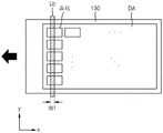
Referring to fig. 1, an embodiment of the display apparatus 100 may include a display area DA and a peripheral area PA over a substrate 130.
On the substrate 130, a plurality of pixels P are arranged in the display area DA. In an exemplary embodiment, as shown in fig. 2, each pixel P may include a pixel circuit PC and an organic light emitting device OLED, which is a display element connected to the pixel circuit PC. The pixel circuit PC may include a first thin film transistor T1, a second thin film transistor T2, and a storage capacitor Cst. Each pixel P may emit, for example, red, green or blue light, or may emit red, green, blue or white light through the organic light emitting device OLED.
The second thin film transistor T2, which is a switching thin film transistor, may be connected to the scan line SL and the data line DL, and may supply the data voltage input from the data line DL to the first thin film transistor T1 based on the switching voltage input from the scan line SL. Here, the scan lines SL may extend in a first direction x, and the data lines DL may extend in a second direction y intersecting the first direction x. The third direction z (shown in fig. 3) may be a direction perpendicular to the first direction x and the second direction y, or a thickness direction of the substrate 130. The storage capacitor Cst may be connected to the second thin film transistor T2 and the driving voltage line PL, and may store a voltage corresponding to a difference between the voltage received from the second thin film transistor T2 and the first power supply voltage ELVDD supplied to the driving voltage line PL.
The first thin film transistor T1, which is a driving thin film transistor, may be connected to the driving voltage line PL and the storage capacitor Cst, and may control a driving current flowing from the driving voltage line PL to the organic light emitting device OLED in response to a voltage value stored in the storage capacitor Cst. The organic light emitting device OLED may emit light having brightness corresponding to the driving current. An electrode (e.g., a cathode) of the organic light emitting device OLED may be supplied with the second power supply voltage ELVSS.
In an embodiment, as shown in fig. 2, the pixel circuit PC may include two thin film transistors and a single storage capacitor, but the embodiment is not limited thereto. The number of thin film transistors and the number of storage capacitors in each pixel circuit PC may be variously modified according to the design of the pixel circuit PC. For example, in one embodiment, the pixel circuit PC may further include one or more thin film transistors in addition to the two thin film transistors described above.
Referring back to fig. 1, a scan driver 180 for supplying a scan signal to each pixel P, a data driver 190 for supplying a data signal to each pixel P, and the like may be disposed in the peripheral area PA on the substrate 130. Fig. 1 shows an embodiment in which the data driver 190 is adjacent to the lateral side of the substrate 130. In an alternative embodiment, the data driver 190 may be disposed on a flexible printed circuit board ("FPCB") electrically connected to pads disposed on the edge of the substrate 130.
A cross-sectional structure of an embodiment of the display device 100 including the thin film transistor 110 will now be described with reference to fig. 3.
Fig. 3 is a sectional view of the display apparatus 100 shown in fig. 1.
Both the first thin film transistor T1 and the second thin film transistor T2 described above with reference to fig. 2 may have a structure corresponding to the thin film transistor 110 shown in fig. 3, but here the thin film transistor 110 may be understood as an embodiment of the first thin film transistor T1, the first thin film transistor T1 being a driving thin film transistor of the organic light emitting device OLED.
In an embodiment, as shown in fig. 3, the display apparatus 100 includes a thin film transistor 110 and an organic light emitting device 120.
The organic light emitting device 120, which is driven by the thin film transistor 110 to display an image by emitting light, includes a pixel electrode 121 and an opposite electrode 123 opposite to each other, and an emission layer 122 between the pixel electrode 121 and the opposite electrode 123.
A predetermined voltage is continuously applied to the opposite electrode 123, and a voltage is selectively applied to the pixel electrode 121 connected to the thin film transistor 110 through the thin film transistor 110. Accordingly, when an appropriate voltage difference is formed between the two electrodes (i.e., the pixel electrode 121 and the opposite electrode 123) based on the selective voltage application of the thin film transistor 110, the emission layer 122 between the pixel electrode 121 and the opposite electrode 123 displays an image by emitting light.
In an embodiment, the thin film transistor 110 has a structure in which an active layer 116, a gate electrode 117, a source electrode 118, and a drain electrode 119 are sequentially stacked one on another over a substrate 130. Accordingly, when an electric signal is applied to the gate electrode 117, a current is allowed to be applied from the source electrode 118 to the drain electrode 119 through the active layer 116, and thus, a voltage is applied to the pixel electrode 121 connected to the drain electrode 119, which results in emission of the above emission layer 122. The structure including the thin film transistor 110 and the substrate 130 may be referred to as a thin film transistor substrate. In addition, the thin film transistor substrate may further include a buffer layer between the substrate 130 and the active layer 116.
In fig. 3, reference numeral 111 denotes a buffer layer between the substrate 130 and the active layer 116, and reference numerals 112, 113, 114, and 115 denote a gate insulating layer, an interlayer insulating layer, a passivation film, and a pixel defining film, respectively.
In an embodiment, a hole injection layer ("HIL"), a hole transport layer ("HTL"), an electron transport layer ("ETL"), an electron injection layer ("EIL"), and the like may be further stacked adjacent to the emission layer 122 in the organic light-emitting device 120. In an embodiment, the emission layer 122 may be separated for each pixel to allow the pixels emitting red, green, and blue light to collectively constitute a unit pixel. Alternatively, the emission layer 122 may be provided in common for the entire pixel area regardless of the position of the pixel. In such an embodiment, in the emission layer 122, layers including light emitting materials for emitting, for example, red, green, and blue light may be vertically stacked, or light emitting materials for emitting, for example, red, green, and blue light may be mixed. Any combination of other various colors capable of emitting white light may be employed. In an embodiment, a color conversion layer or a color filter for converting the emitted white light into a certain color may be further included. In an embodiment, a thin film encapsulation layer (not shown) including organic and inorganic films alternately stacked may be on the opposite electrode 123.
In an embodiment, when the active layer 116 is formed, the following process is performed: an amorphous silicon layer is formed on the buffer layer 111 disposed on the substrate 130, and then the amorphous silicon layer is changed into a crystalline silicon layer by crystallizing the amorphous silicon layer through a heat treatment, and during such a heat treatment, crystal grains collide with each other while growing, and thus, a protrusion 1 may be formed at a boundary thereof (refer to fig. 4F). When the protrusion 1 is too long, an electric field is concentrated thereon, and thus, as described above, a deviation in electrical characteristics of the device may be increased, thereby causing undesirable instability. Also, the protrusions 1 may be perceived by the user as a pattern, such as a moire pattern, as if there were undesirable spots on the screen. Accordingly, in the embodiment of the present invention, the following manufacturing process may be performed for regulating the height of the protrusion 1 (refer to fig. 4F) of the active layer 116 to an appropriate height to effectively prevent the above problem.
Fig. 4A to 4H show an embodiment of a modified manufacturing process to control the height of the protrusion 1 of the active layer 116 to be equal to or less than the appropriate height as described above.
In an embodiment, as shown in fig. 4A, a buffer layer 111 is provided or formed on a substrate 130. In this embodiment, buffer layer 111 comprises SiOxAnd has a thickness of about 4000 angstroms To about
 Wherein "x" can be greater than 0 and less than or equal to 2 (i.e., 0)<x is less than or equal to 2). Generally, SiNxFor forming the
 buffer layer 111, but SiNxMuch hydrogen is contained, and accordingly, a large amount of hydrogen may permeate into the active layer 116 during a crystallization process described below, thereby causing a problem in characteristics of the active layer 116. Accordingly, in embodiments, SiO with a low hydrogen content is usedxAnd is measured by To about
 A small thickness in the range of (1) forms the
 buffer layer 111.
In an embodiment, as shown in fig. 4B, an amorphous silicon layer 116(a) to be formed as an active layer 116 is provided or formed on the buffer layer 111, and the amorphous silicon layer 116(a) is also thin enough to have about the thickness of the active layer 116(a) To about
 A thickness within the range of (1). In an embodiment, in the case where the amorphous silicon layer 116(a) is thick, for example, thicker than the thickness in the above range, the
 protrusion 1 may become larger later, and thus, the amorphous silicon layer 116(a) is formed substantially in a small thickness.
In this embodiment, as shown in fig. 4B, the oxide film 116-1 is naturally formed on the amorphous silicon layer 116 (a). Accordingly, the oxide film 116-1 is first removed before the crystallization is performed. If cleaned by conventional water or ozone (O)3) Cleaning removes the oxide film 116-1, the oxide film 116-1 may not be completely removed and may leave a residue thereof everywhere, so that the residue of the oxide film 116-1 may cause the protrusion 1 of the active layer 116 to rise after crystallization. The reason for this will be described later.
Accordingly, in an embodiment, as shown in fig. 4C, a hydrogen fluoride solution containing about 0.5 volume percent (vol%) of Hydrogen Fluoride (HF) is sprayed onto the oxide film 116-1 for about 60 seconds to about 120 seconds to effectively completely remove the oxide film 116-1, and thus, the oxide film 116-1 by a chemical reaction. When the hydrogen fluoride solution is sprayed as described above, the oxide film 116-1 can be effectively and completely removed without leaving a residue.
In an embodiment, as shown in fig. 4D, a first rinsing cleaning is performed on the surface of the amorphous silicon layer 116(a) from which the oxide film 116-1 is removed with hydrogen water DIW containing about one part per million (ppm) of hydrogen. In this embodiment, the hydrogen water DIW is not ejected, but drops in a free-falling form to flow over the surface of the amorphous silicon layer 116 (a). The hydrogen water DIW is a liquid containing about 1ppm of hydrogen and no oxygen, and accordingly, although cleaning is performed using the hydrogen water DIW, an oxide film is not formed again on the surface of the amorphous silicon layer 116 (a). However, when the hydrogen water DIW is ejected, the surface area of the liquid particles dispersed in the liquid droplets increases drastically, and therefore, the chance of oxygen being mixed therewith increases. Accordingly, formation of a second oxide film may be caused. Accordingly, in the embodiment, the surface of the amorphous silicon layer 116(a) is rinse cleaned by supplying the hydrogen water DIW in a free-falling form instead of spraying the hydrogen water DIW.
In an embodiment, a second rinse clean is performed as shown in fig. 4E. In this embodiment, the second rinsing cleaning is substantially the same as the first rinsing cleaning including supplying the hydrogen water DIW containing 1ppm of hydrogen in a free-falling form, except that the hydrogen water DIW is supplied by adding vibration to the hydrogen water DIW with megasonic waves. In such an embodiment, the flushing effect may be further enhanced as the liquid particles of the hydrogen water DIW vibrate.
When the amorphous silicon layer 116(a) from which the oxide film 116-1 is completely removed without leaving a residue is prepared by the above process, as shown in fig. 4F, a heat treatment process is performed for changing the amorphous silicon layer 116(a) into the crystalline silicon layer 116(P) by radiating a laser beam and heating the amorphous silicon layer 116(a) at a crystallization temperature or higher. The laser beam may be, for example, an excimer laser beam.
In this embodiment, as described above, as the grains grow through the melting and solidification process and collide at the grain boundaries, the protrusions 1 are formed. In this embodiment, since the residue of the oxide film 116-1 on the surface of the amorphous silicon layer 116(a) has been effectively completely removed and, therefore, heat is uniformly transferred throughout the entire region, the height h1 of the protrusion 1 is effectively maintained at about 3 nanometers (nm) or less. Here, the height h1 of the protrusion 1 is defined as a distance between the highest point and the lowest point of the upper surface of the crystalline silicon layer 116 (P).
Hereinafter, embodiments of the present invention will be described with reference to a comparative example using a conventional heat treatment in which a residue of the oxide film 116-1 is left.
Fig. 5A and 5B are sectional views showing a conventional method as a comparative example in which the amorphous silicon layer 116(a) is crystallized without removing the oxide film 116-1.
As shown in fig. 5A, in the case where the removal operation by the hydrogen fluoride solution is not performed, and therefore, a residue of the oxide film 116-1 is left everywhere on the surface of the amorphous silicon layer 116(a), a local deviation occurs only due to heat transfer into the amorphous silicon layer 116(a) during irradiation of the laser beam, and a local deviation occurs only due to heat dissipation during curing. That is, since the heat flows unstably in the region shielded by the residue of the oxide film 116-1 and the flow of the heat is relatively stable in the region not shielded by the residue of the oxide film 116-1, crystallization proceeds more rapidly where the heat flows smoothly, and therefore, the height h2 of the protrusion 1 becomes relatively much larger. In this case, when the residue of the oxide film 116-1 is left, the height h2 of the protrusion 1 may be in the range of about 14nm to about 16 nm. As a result, the characteristics of the active layer 116 for the thin film transistor may later become problematic, and further, the protrusion 1 may be large enough to be perceived as a spot by a user, which may reduce product quality.
In the embodiment of the invention, as described above, the crystallization heat treatment process is performed after the oxide film 116-1 is sufficiently removed with the hydrogen fluoride solution, so that the height h1 of the protrusion 1 can be controlled to about 3nm or less, and thus, the product quality can be improved.
The irradiation process of the laser beam will be described in detail with reference to fig. 6.
After the above-described crystallization heat treatment process is completed, as shown in fig. 4G, the crystalline silicon layer 116(P) is patterned to have the size of the active layer 116 of the thin film transistor 110.
In the embodiment, as shown in fig. 4H, a gate electrode 117 is formed to face the active layer 116 with the gate insulating layer 112 between the gate electrode 117 and the active layer 116, and an interlayer insulating layer 113, a source electrode 118, and a drain electrode 119 are provided or formed.
Accordingly, the thin film transistor 110 having improved characteristics without undesirable factors such as an electric field concentration or a visible spot pattern on a certain area is formed, and when the organic light emitting device 120 is subsequently formed, the display apparatus 100 shown in fig. 3 is manufactured.
According to the experiment, the spot pattern is reduced by about 20% as compared with the thin film transistor manufactured by the conventional method, so that the spot pattern is substantially hardly visible to the naked eye, and the deviation of the electrical characteristics of the region of the thin film transistor is also improved by about 20% to about 45% to become highly uniform. Accordingly, when the thin film transistor 110 and the display device 100 described above are implemented, the quality thereof can be effectively and stably obtained.
When a laser beam is irradiated to crystallize the amorphous silicon layer 116(a), the irradiation method shown in fig. 6 may be used.
A plurality of unit cells targeted for crystallization are aligned over the substrate 130 in the first direction x and the second direction y, and each unit cell may be understood as a region corresponding to a cell of the amorphous silicon layer 116(a) targeted for crystallization in the display area DA.
The laser beam Lb is irradiated onto the unit cells disposed above the substrate 130 in the form of a rectangle having a long side in the second direction y of fig. 6 and a short side in the first direction x of fig. 6, and the laser beam Lb is irradiated onto the entire area of each unit cell as the substrate 130 is moved by a predetermined pitch in the first direction x. The short side width W1 of the laser beam Lb is about 480 micrometers (μm), and the laser beam Lb is irradiated with an energy of about 440 millijoules (mJ) to about 480 mJ. The laser beam is not maintained in an on state, but is repeatedly turned on/off every time the substrate 130 moves by a certain pitch.
In the embodiment, the moving direction (x) of the substrate 130 and the long side direction (y) of the laser beam Lb are perpendicular to each other. In this embodiment, the laser irradiation work may be performed so that the moving direction (x) of the substrate 130 and the long side direction (y) of the laser beam Lb are perpendicular to each other. In the embodiment of the invention, since the height of the protrusion 1 is about 3nm or less, the moving direction (x) of the substrate 130 and the long side direction (y) of the laser beam Lb are allowed to be perpendicular to each other in the laser beam irradiation process.
In the related art, when the protrusion 1 is high enough to reach about 15nm, the height of the protrusion 1 itself may be sufficient to allow the user to perceive the protrusion 1 as a spot, and the spot may look larger when an effect caused by an energy deviation due to the on/off of the laser beam Lb is added thereto.
That is, when the laser beam Lb is turned on, the central region receives relatively more energy than the edge region, and when the laser beam Lb is turned on again after moving by a certain pitch, the central region receives relatively more energy than the edge region again, and therefore, the deviation may cause a difference in the degree of crystallization between the central region and the edge region, and a stripe pattern extending in the second direction y may repeatedly appear in the first direction x. The stripe pattern itself may not be clearly visible to the user; however, when the stripe pattern is combined with the spot pattern due to the significant height of the protrusions 1, the stripe pattern may cause the spot pattern to be more clearly seen. Accordingly, in the conventional method, the long side of the laser beam Lb and the moving direction of the substrate 130 are allowed to form 89 degrees, which is inclined by 1 degree with respect to 90 degrees, to perform crystallization, to solve the above problem. Since the projections 1 are formed in the unit cells arranged in the direction x and the direction y, the stripe pattern due to the radiation deviation of the laser beam Lb is slightly inclined, not aligned with the direction x and the direction y. Therefore, the spot pattern due to the significant height of the protrusions 1 and the stripe pattern due to the radiation deviation of the laser beam Lb may not be aligned precisely.
However, when the laser beam Lb is inclined to prevent the long side of the laser beam Lb and the moving direction of the substrate 130 from being perpendicular to each other, the laser beam Lb moves diagonally on the substrate 130, and thus, a dead space not in contact with the laser beam Lb is increased in the substrate 130. That is, the area of the substrate 130 may not be effectively used.
In the embodiment of the present invention, as described above, the height of the protrusion 1 may be controlled to about 3nm or less, and thus, the protrusion 1 may not be visible to the user although combined with the stripe pattern due to the energy deviation of the laser beam Lb. Accordingly, as shown in fig. 6, the laser irradiation work may be performed so that the moving direction (x) of the substrate 130 and the long side direction (y) of the laser beam Lb are perpendicular to each other.
The stripe pattern due to the energy deviation of the laser beam Lb can also be reduced, and for this purpose, the shift pitch can be set to turn on the laser beam Lb at least 7 times for one unit cell. The turned-on laser beam Lb is generally referred to as shot, and the moving pitch of the substrate 130 is set to make 7 or more close shots in one unit cell. In one embodiment, for example, when the movement pitch is set in the range of about 1 μm to about 68 μm, the laser beam Lb having a short side of about 480 μm is used, generally at least 7 shots can be performed in one unit cell, and accordingly, the stripe pattern due to the energy deviation of the laser beam Lb can also be reduced.
Accordingly, when using the embodiments of the thin film transistor substrate, the display device including the thin film transistor substrate, and the manufacturing method of the thin film transistor substrate and the display device, by reducing the size of the protrusion formed at the grain boundary of the active layer, it is possible to solve an excessive concentration of an electric field on the protrusion and a screen quality failure due to the visibility of a speckle pattern, and thus, quality and reliability of a product can be obtained.
It is to be understood that the embodiments described herein are to be considered in a descriptive sense only and not for purposes of limitation. Descriptions of features or aspects in each embodiment should generally be considered as available for other similar features or aspects in other embodiments. While one or more embodiments have been described with reference to the accompanying drawings, it will be understood by those of ordinary skill in the art that various changes in form and details may be made therein without departing from the spirit and scope defined by the following claims.
Claims (20)


Applications Claiming Priority (2)
| Application Number | Priority Date | Filing Date | Title |
|---|---|---|---|
| KR10-2019-0084545 | 2019-07-12 | ||
| KR1020190084545A KR102738040B1 (en) | 2019-07-12 | 2019-07-12 | Thin film transistor and display apparatus including the same and the manufacturing method thereof |
Publications (2)
| Publication Number | Publication Date |
|---|---|
| CN112216612A true CN112216612A (en) | 2021-01-12 |
| CN112216612B CN112216612B (en) | 2026-04-21 |
Family
ID=74059527
Family Applications (1)
| Application Number | Title | Priority Date | Filing Date |
|---|---|---|---|
| CN202010655636.5A Active CN112216612B (en) | 2019-07-12 | 2020-07-09 | Thin-film transistor substrates, display devices including them, and methods for manufacturing them. |
Country Status (4)
| Country | Link |
|---|---|
| US (1) | US11329117B2 (en) |
| JP (1) | JP7688468B2 (en) |
| KR (1) | KR102738040B1 (en) |
| CN (1) | CN112216612B (en) |
Families Citing this family (2)
| Publication number | Priority date | Publication date | Assignee | Title |
|---|---|---|---|---|
| KR20230068697A (en) * | 2021-11-11 | 2023-05-18 | 엘지디스플레이 주식회사 | Organic Light Emitting Diode display apparatus |
| US20260068553A1 (en) * | 2024-09-04 | 2026-03-05 | Applied Materials, Inc. | Ion Beam-Induced Epitaxial Crystallization on an Integrated Processing Architecture |
Citations (5)
| Publication number | Priority date | Publication date | Assignee | Title |
|---|---|---|---|---|
| US20040127032A1 (en) * | 2002-12-31 | 2004-07-01 | Au Optronics Corp. | Process for cleaning silicon surface and fabrication of thin film transistor by the process |
| JP2006332589A (en) * | 2005-04-25 | 2006-12-07 | Toshiba Matsushita Display Technology Co Ltd | Method and apparatus for controlling film |
| CN102270570A (en) * | 2010-06-03 | 2011-12-07 | 三星移动显示器株式会社 | Method of crystallizing silicon layer and method of forming thin film transistor using same |
| CN104779139A (en) * | 2015-03-31 | 2015-07-15 | 深超光电(深圳)有限公司 | Manufacturing method of semi-conductor thin film and manufacturing method of thin film transistor |
| CN106910749A (en) * | 2017-04-19 | 2017-06-30 | 京东方科技集团股份有限公司 | Low-temperature polycrystalline silicon layer and preparation method, display base plate and display device |
Family Cites Families (19)
| Publication number | Priority date | Publication date | Assignee | Title |
|---|---|---|---|---|
| KR100299292B1 (en) | 1993-11-02 | 2001-12-01 | 이데이 노부유끼 | Polysilicon Thin Film Forming Method and Surface Treatment Apparatus |
| JPH11251599A (en) * | 1998-03-06 | 1999-09-17 | Toshiba Corp | Method for manufacturing thin film semiconductor device |
| JP2001035824A (en) * | 1999-07-21 | 2001-02-09 | Matsushita Electronics Industry Corp | Method of cleaning substrate and apparatus for cleaning substrate |
| JP2001274085A (en) * | 2000-03-27 | 2001-10-05 | Fujitsu Ltd | Polycrystalline silicon thin film, manufacturing method thereof, thin film transistor, liquid crystal display device, and system on panel |
| JP4919546B2 (en) * | 2000-09-18 | 2012-04-18 | 東芝モバイルディスプレイ株式会社 | Method for forming polycrystalline silicon film |
| JP2003119494A (en) * | 2001-10-05 | 2003-04-23 | Nec Corp | Washing composition, and washing method and washing device using the same |
| JP2003124231A (en) * | 2001-10-12 | 2003-04-25 | Seiko Epson Corp | Method of manufacturing thin film transistor, electronic apparatus, and electro-optical device |
| CN101009322B (en) * | 2001-11-09 | 2012-06-27 | 株式会社半导体能源研究所 | Light-emitting device |
| JP4149168B2 (en) * | 2001-11-09 | 2008-09-10 | 株式会社半導体エネルギー研究所 | Light emitting device |
| JP2005085981A (en) * | 2003-09-09 | 2005-03-31 | Matsushita Electric Ind Co Ltd | Manufacturing method and cleaning method of electronic device |
| JP2006272069A (en) * | 2005-03-28 | 2006-10-12 | Kurita Water Ind Ltd | Cleaning device |
| US20060240647A1 (en) * | 2005-04-25 | 2006-10-26 | Toshiba Matsushita Display Technology Co., Ltd. | Film control method and device thereof |
| JP2007027270A (en) * | 2005-07-13 | 2007-02-01 | Sony Corp | Cleaning device and cleaning method |
| JP5041255B2 (en) * | 2007-04-18 | 2012-10-03 | 三菱電機株式会社 | Manufacturing method of semiconductor thin film |
| KR100874457B1 (en) | 2007-06-25 | 2008-12-17 | 삼성모바일디스플레이주식회사 | Manufacturing method of organic light emitting display device |
| KR101108169B1 (en) | 2010-03-11 | 2012-01-31 | 삼성모바일디스플레이주식회사 | Continuous side crystallization mask and continuous side crystallization apparatus having the same |
| CN103762178A (en) | 2013-12-25 | 2014-04-30 | 深圳市华星光电技术有限公司 | LTPS TFT and manufacturing method thereof |
| US9257290B2 (en) | 2013-12-25 | 2016-02-09 | Shenzhen China Star Optoelectronics Technology Co., Ltd. | Low temperature poly-silicon thin film transistor and manufacturing method thereof |
| JP2017098290A (en) * | 2015-11-18 | 2017-06-01 | 富士フイルム株式会社 | Manufacturing method of display element |
-
2019
- 2019-07-12 KR KR1020190084545A patent/KR102738040B1/en active Active
-
2020
- 2020-05-19 US US16/877,735 patent/US11329117B2/en active Active
- 2020-06-05 JP JP2020098474A patent/JP7688468B2/en active Active
- 2020-07-09 CN CN202010655636.5A patent/CN112216612B/en active Active
Patent Citations (5)
| Publication number | Priority date | Publication date | Assignee | Title |
|---|---|---|---|---|
| US20040127032A1 (en) * | 2002-12-31 | 2004-07-01 | Au Optronics Corp. | Process for cleaning silicon surface and fabrication of thin film transistor by the process |
| JP2006332589A (en) * | 2005-04-25 | 2006-12-07 | Toshiba Matsushita Display Technology Co Ltd | Method and apparatus for controlling film |
| CN102270570A (en) * | 2010-06-03 | 2011-12-07 | 三星移动显示器株式会社 | Method of crystallizing silicon layer and method of forming thin film transistor using same |
| CN104779139A (en) * | 2015-03-31 | 2015-07-15 | 深超光电(深圳)有限公司 | Manufacturing method of semi-conductor thin film and manufacturing method of thin film transistor |
| CN106910749A (en) * | 2017-04-19 | 2017-06-30 | 京东方科技集团股份有限公司 | Low-temperature polycrystalline silicon layer and preparation method, display base plate and display device |
Also Published As
| Publication number | Publication date |
|---|---|
| KR102738040B1 (en) | 2024-12-06 |
| JP7688468B2 (en) | 2025-06-04 |
| US20210013281A1 (en) | 2021-01-14 |
| US11329117B2 (en) | 2022-05-10 |
| CN112216612B (en) | 2026-04-21 |
| JP2021015958A (en) | 2021-02-12 |
| KR20210008264A (en) | 2021-01-21 |
Similar Documents
| Publication | Publication Date | Title |
|---|---|---|
| US8467023B2 (en) | Anti-reflection film and display device | |
| CN1744283B (en) | Manufacturing method of semiconductor device | |
| CN100437976C (en) | Display device, manufacturing method thereof, and television receiver | |
| CN100481560C (en) | Matrix display element and method for manufacturing the same | |
| TWI356497B (en) | Display device and method for fabricating the same | |
| JP7536079B2 (en) | Inkjet printing device, method for aligning bipolar elements, and method for manufacturing a display device | |
| JP5298098B2 (en) | Method for manufacturing semiconductor device | |
| KR20150075017A (en) | Organic light emitting display device, method for repair of the same and | |
| JP4853607B2 (en) | Thin film transistor manufacturing method | |
| CN112216612B (en) | Thin-film transistor substrates, display devices including them, and methods for manufacturing them. | |
| CN1536542A (en) | Flat panel display with thin film transistors | |
| US7384862B2 (en) | Method for fabricating semiconductor device and display device | |
| KR100646297B1 (en) | Method of manufacturing display device | |
| JP4393968B2 (en) | Wiring manufacturing method and semiconductor device manufacturing method | |
| CN112928186A (en) | Method of aligning light emitting elements, method of manufacturing display device, and display device | |
| KR102519086B1 (en) | Organic light emitting diode display and method for manufacturing the same | |
| CN100592478C (en) | Thin film transistor, display device and liquid crystal display device, and method of manufacturing the same | |
| US7297622B2 (en) | Wiring method | |
| JP2008234932A (en) | Display device | |
| KR20190122455A (en) | Display device having an auxiliary electrode | |
| JP2006294446A (en) | Electro-optical device, method of manufacturing electro-optical device, and electronic apparatus | |
| US8703589B2 (en) | Flat panel display and method of manufacturing the same | |
| CN100440437C (en) | Manufacturing method of thin film transistor, electro-optical device and electronic instrument | |
| JP2007095610A (en) | LIGHT EMITTING DEVICE MANUFACTURING METHOD AND LIGHT EMITTING DEVICE | |
| JP2005039261A (en) | Method of manufacturing semiconductor device and display device |
Legal Events
| Date | Code | Title | Description |
|---|---|---|---|
| PB01 | Publication | ||
| PB01 | Publication | ||
| SE01 | Entry into force of request for substantive examination | ||
| SE01 | Entry into force of request for substantive examination | ||
| GR01 | Patent grant |