CN112134458A - Switched parallel regulator circuit - Google Patents
Switched parallel regulator circuit Download PDFInfo
- Publication number
- CN112134458A CN112134458A CN202010850845.5A CN202010850845A CN112134458A CN 112134458 A CN112134458 A CN 112134458A CN 202010850845 A CN202010850845 A CN 202010850845A CN 112134458 A CN112134458 A CN 112134458A
- Authority
- CN
- China
- Prior art keywords
- current
- voltage
- output
- inductor
- coupled
- Prior art date
- Legal status (The legal status is an assumption and is not a legal conclusion. Google has not performed a legal analysis and makes no representation as to the accuracy of the status listed.)
- Pending
Links
- 239000000872 buffer Substances 0.000 claims description 53
- 230000033228 biological regulation Effects 0.000 claims description 30
- 238000000034 method Methods 0.000 claims description 15
- 230000005669 field effect Effects 0.000 claims description 9
- 229910044991 metal oxide Inorganic materials 0.000 claims description 9
- 150000004706 metal oxides Chemical class 0.000 claims description 9
- 239000004065 semiconductor Substances 0.000 claims description 9
- 230000001105 regulatory effect Effects 0.000 claims description 7
- 230000008878 coupling Effects 0.000 claims description 4
- 238000010168 coupling process Methods 0.000 claims description 4
- 238000005859 coupling reaction Methods 0.000 claims description 4
- 230000008859 change Effects 0.000 claims description 3
- 230000001276 controlling effect Effects 0.000 claims description 3
- 238000010586 diagram Methods 0.000 description 10
- 239000003990 capacitor Substances 0.000 description 5
- 230000001934 delay Effects 0.000 description 3
- 238000006243 chemical reaction Methods 0.000 description 2
- 230000001351 cycling effect Effects 0.000 description 2
- 238000005516 engineering process Methods 0.000 description 2
- 230000005355 Hall effect Effects 0.000 description 1
- 240000007594 Oryza sativa Species 0.000 description 1
- 235000007164 Oryza sativa Nutrition 0.000 description 1
- 230000008901 benefit Effects 0.000 description 1
- 230000015556 catabolic process Effects 0.000 description 1
- 230000003750 conditioning effect Effects 0.000 description 1
- 230000007423 decrease Effects 0.000 description 1
- 238000006731 degradation reaction Methods 0.000 description 1
- 230000005611 electricity Effects 0.000 description 1
- 238000002955 isolation Methods 0.000 description 1
- 230000003071 parasitic effect Effects 0.000 description 1
- 230000008569 process Effects 0.000 description 1
- 235000009566 rice Nutrition 0.000 description 1
Images




Classifications
-
- H—ELECTRICITY
- H02—GENERATION; CONVERSION OR DISTRIBUTION OF ELECTRIC POWER
- H02M—APPARATUS FOR CONVERSION BETWEEN AC AND AC, BETWEEN AC AND DC, OR BETWEEN DC AND DC, AND FOR USE WITH MAINS OR SIMILAR POWER SUPPLY SYSTEMS; CONVERSION OF DC OR AC INPUT POWER INTO SURGE OUTPUT POWER; CONTROL OR REGULATION THEREOF
- H02M3/00—Conversion of DC power input into DC power output
- H02M3/02—Conversion of DC power input into DC power output without intermediate conversion into AC
- H02M3/04—Conversion of DC power input into DC power output without intermediate conversion into AC by static converters
- H02M3/10—Conversion of DC power input into DC power output without intermediate conversion into AC by static converters using discharge tubes with control electrode or semiconductor devices with control electrode
- H02M3/145—Conversion of DC power input into DC power output without intermediate conversion into AC by static converters using discharge tubes with control electrode or semiconductor devices with control electrode using devices of a triode or transistor type requiring continuous application of a control signal
- H02M3/155—Conversion of DC power input into DC power output without intermediate conversion into AC by static converters using discharge tubes with control electrode or semiconductor devices with control electrode using devices of a triode or transistor type requiring continuous application of a control signal using semiconductor devices only
- H02M3/156—Conversion of DC power input into DC power output without intermediate conversion into AC by static converters using discharge tubes with control electrode or semiconductor devices with control electrode using devices of a triode or transistor type requiring continuous application of a control signal using semiconductor devices only with automatic control of output voltage or current, e.g. switching regulators
- H02M3/158—Conversion of DC power input into DC power output without intermediate conversion into AC by static converters using discharge tubes with control electrode or semiconductor devices with control electrode using devices of a triode or transistor type requiring continuous application of a control signal using semiconductor devices only with automatic control of output voltage or current, e.g. switching regulators including plural semiconductor devices as final control devices for a single load
-
- H—ELECTRICITY
- H02—GENERATION; CONVERSION OR DISTRIBUTION OF ELECTRIC POWER
- H02M—APPARATUS FOR CONVERSION BETWEEN AC AND AC, BETWEEN AC AND DC, OR BETWEEN DC AND DC, AND FOR USE WITH MAINS OR SIMILAR POWER SUPPLY SYSTEMS; CONVERSION OF DC OR AC INPUT POWER INTO SURGE OUTPUT POWER; CONTROL OR REGULATION THEREOF
- H02M1/00—Details of apparatus for conversion
- H02M1/0045—Converters combining the concepts of switch-mode regulation and linear regulation, e.g. linear pre-regulator to switching converter, linear and switching converter in parallel, same converter or same transistor operating either in linear or switching mode
Landscapes
- Engineering & Computer Science (AREA)
- Power Engineering (AREA)
- Dc-Dc Converters (AREA)
Abstract
一种开关式并联调节器电路包括:电流源,所述电流源具有用于接收输入电压的输入端和用于提供DC电流的输出端;以及联接至所述电流源的所述输出端的并联电压调节器。当DC负载被联接至所述输出端时,所述电流源被配置成向所述DC负载提供DC电流,并向所述并联电压调节器提供DC电流。提供给所述并联电压调节器的DC电流调节在所述输出端的电压。所述并联电压调节器具有的载流容量大于提供给所述DC负载的DC电流和提供给所述并联电压调节器的DC电流的总和。

A switching shunt regulator circuit includes: a current source having an input terminal for receiving an input voltage and an output terminal for providing a DC current; and a shunt voltage regulator connected to the output terminal of the current source. When a DC load is connected to the output terminal, the current source is configured to provide a DC current to the DC load and to provide a DC current to the shunt voltage regulator. The DC current provided to the shunt voltage regulator regulates the voltage at the output terminal. The shunt voltage regulator has a current carrying capacity greater than the sum of the DC current provided to the DC load and the DC current provided to the shunt voltage regulator.
Description
本申请是申请日为2014年12月8日、申请号为201410742865.5、发明名称为“开关式并联调节器电路”的原案申请的分案申请。This application is a divisional application of the original application whose filing date is December 8, 2014, the application number is 201410742865.5, and the invention name is "switched parallel regulator circuit".
相关申请的交叉引用CROSS-REFERENCE TO RELATED APPLICATIONS
本申请要求2013年12月6日递交的第61/913,053号美国临时申请的权益。上述申请的全部公开内容以引用的方式并入本文。This application claims the benefit of US Provisional Application No. 61/913,053, filed December 6, 2013. The entire disclosures of the above applications are incorporated herein by reference.
技术领域technical field
本公开涉及开关式并联调节器电路。The present disclosure relates to switched shunt regulator circuits.
背景技术Background technique
本部分提供与本公开相关的背景信息,其不一定是现有技术。This section provides background information related to the present disclosure which is not necessarily prior art.
数字控制技术可用来取代电子产品中的模拟电路,该电子产品例如是可包含智能控制功能和远程控制功能的简单的家用电器。这些智能特征需要要求稳定的偏置功率的微处理器。数控电源也需要待被首先通电的微处理器或数字信号处理器,以便允许受控操作。Digital control technology can be used to replace analog circuits in electronic products, such as simple household appliances that can include intelligent control functions and remote control functions. These smart features require microprocessors that require stable bias power. Digitally controlled power supplies also require a microprocessor or digital signal processor to be powered up first in order to allow controlled operation.
直接从公用电网电源(例如,115VAC、230VAC等)获得低的偏置电压(例如,3.3V)是具有挑战的。例如,典型的单相家庭电度表可在3.3V下仅需要约10mA。降压转换器可需要极其小的占空比,以从公用电网电源产生这样的低偏置电压。许多应用针对于转换器不允许低压侧控制开关操作,并且高压侧开关操作针对于调节需要高压侧驱动和直接感测输出电压的相关难度。在续流期间的间接反馈不提供对于微处理器所需要的紧压调节。针对低功率需求,使用用于调节的光耦合器增加了成本和复杂性。Obtaining low bias voltages (eg, 3.3V) directly from utility grid power (eg, 115VAC, 230VAC, etc.) is challenging. For example, a typical single-phase household watt-hour meter may only require about 10mA at 3.3V. Buck converters may require extremely small duty cycles to generate such low bias voltages from utility grid power. Many applications for converters do not allow low-side controlled switching operations, and high-side switching operations for regulation require high-side drive and the associated difficulty of directly sensing the output voltage. Indirect feedback during freewheeling does not provide the tight pressure regulation required for the microprocessor. For low power requirements, the use of optocouplers for conditioning adds cost and complexity.
发明内容SUMMARY OF THE INVENTION
本部分提供本公开的总体概述,并不是其全部范围或其全部特征的全面公开。This section provides a general overview of the disclosure, and is not a comprehensive disclosure of its full scope or all of its features.
概念1:一种开关式并联调节器电路包括:电流源,所述电流源具有用于接收输入电压的输入端和用于提供DC(直流)电流的输出端;以及联接至所述电流源的所述输出端的并联电压调节器。当DC负载被联接至所述输出端时,所述电流源被配置成向所述DC负载提供DC电流,并向所述并联电压调节器提供DC电流。提供给所述并联电压调节器的DC电流调节在所述输出端的电压。所述并联电压调节器具有的载流容量大于提供给所述DC负载的DC电流和提供给所述并联电压调节器的DC电流的总和。Concept 1: A switched shunt regulator circuit comprising: a current source having an input for receiving an input voltage and an output for providing a DC (direct current) current; and a current source coupled to the current source a parallel voltage regulator at the output. When a DC load is coupled to the output, the current source is configured to provide DC current to the DC load and to provide DC current to the parallel voltage regulator. The DC current provided to the parallel voltage regulator regulates the voltage at the output. The shunt voltage regulator has a current carrying capacity greater than the sum of the DC current supplied to the DC load and the DC current supplied to the shunt voltage regulator.
概念2:根据概念1所述的开关式并联调节器电路,其中,所述电流源包括开关、电感器和开关控制器,所述开关控制器被配置成当通过所述电感器的电流达到下限阈值时接通所述开关、当通过所述电感器的所述电流达到上限阈值时关断所述开关。Concept 2: The switched shunt regulator circuit of
概念3:根据前述概念中任一项所述的开关式并联调节器电路,其中,所述下限阈值约为零,并且所述开关控制器被配置成运行所述开关以使所述电感器在边界模式操作下运行,其中,通过所述电感器的所述电流在大约零和峰值之间循环。Concept 3: The switched shunt regulator circuit of any one of the preceding concepts, wherein the lower threshold is approximately zero and the switch controller is configured to operate the switch such that the inductor is at Operating in boundary mode operation, wherein the current through the inductor cycles between approximately zero and a peak value.
概念4:根据前述概念中任一项所述的开关式并联调节器电路,其中,所述电流源包括联接至所述开关控制器的电流感测器,所述电流感测器被配置成感测通过所述电感器的电流,所述开关控制器联接至所述开关并且被配置成当感测到的通过所述电感器的电流达到下限阈值时接通所述开关、当感测到的通过所述电感器的电流达到上限阈值时关断所述开关。Concept 4: The switched shunt regulator circuit of any one of the preceding concepts, wherein the current source includes a current sensor coupled to the switching controller, the current sensor configured to sense measuring current through the inductor, the switch controller coupled to the switch and configured to turn on the switch when the sensed current through the inductor reaches a lower threshold, and when the sensed current through the inductor reaches a lower threshold The switch is turned off when the current through the inductor reaches an upper threshold.
概念5:根据前述概念中任一项所述的开关式并联调节器电路,其中,所述开关控制器为具有高输入滞后阈值和低输入滞后阈值的缓冲器。Concept 5: The switched shunt regulator circuit of any of the preceding concepts, wherein the switching controller is a buffer having a high input hysteresis threshold and a low input hysteresis threshold.
概念6:根据前述概念中任一项所述的开关式并联调节器电路,其中,所述电路为非隔离式电路。Concept 6: The switched shunt regulator circuit of any one of the preceding concepts, wherein the circuit is a non-isolated circuit.
概念7:根据前述概念中任一项所述的开关式并联调节器电路,其中,所述电路包括电感器、开关、二极管、具有高输入滞后阈值和低输入滞后阈值的缓冲器、和电流感测器。Concept 7: The switched shunt regulator circuit of any one of the preceding concepts, wherein the circuit includes an inductor, a switch, a diode, a snubber with a high input hysteresis threshold and a low input hysteresis threshold, and a current sense tester.
概念8:根据前述概念中任一项所述的开关式并联调节器电路,其中,至少所述开关、所述二极管和所述缓冲器被包括在集成电路中。Concept 8: The switched shunt regulator circuit of any one of the preceding concepts, wherein at least the switch, the diode and the snubber are included in an integrated circuit.
概念9:根据前述概念中任一项所述的开关式并联调节器电路,其中,所述电流源包括集成电路。Concept 9: The switched shunt regulator circuit of any of the preceding concepts, wherein the current source comprises an integrated circuit.
概念10:根据前述概念中任一项所述的开关式并联调节器电路,其中,所述并联电压调节器包括齐纳二极管。Concept 10: The switched shunt regulator circuit of any of the preceding concepts, wherein the shunt voltage regulator includes a Zener diode.
概念11:根据前述概念中任一项所述的开关式并联调节器电路,其中,所述电流源被配置成利用所述输出端的电压作为用于所述缓冲器的偏置电源电压。Concept 11: The switched shunt regulator circuit of any one of the preceding concepts, wherein the current source is configured to utilize the voltage at the output as a bias supply voltage for the buffer.
概念12:根据前述概念中任一项所述的开关式并联调节器电路,其中,所述电流源包括金属氧化物半导体场效应晶体管(MOSFET)。Concept 12: The switched shunt regulator circuit of any of the preceding concepts, wherein the current source comprises a metal oxide semiconductor field effect transistor (MOSFET).
概念13:根据前述概念中任一项所述的开关式并联调节器电路,其中,所述电流源包括发射极开关的双极晶体管开关,所述发射极开关的双极晶体管开关具有与低额定电压的金属氧化物半导体场效应晶体管(MOSFET)串联的双极结晶体管(BJT)。Concept 13: The switched shunt regulator circuit of any one of the preceding concepts, wherein the current source comprises an emitter-switched bipolar transistor switch having an emitter-switched bipolar transistor switch with a low rating Voltage metal oxide semiconductor field effect transistors (MOSFETs) in series with bipolar junction transistors (BJTs).
概念14:根据前述概念中任一项所述的开关式并联调节器电路,其中,所述电流源的所述输入端通过整流器联接至公用电网。Concept 14: The switched shunt regulator circuit of any one of the preceding concepts, wherein the input of the current source is coupled to a utility grid through a rectifier.
概念15:根据前述概念中任一项所述的开关式并联调节器电路,其中,所述电流源的所述输出端联接至数字控制器。Concept 15: The switched shunt regulator circuit of any one of the preceding concepts, wherein the output of the current source is coupled to a digital controller.
概念16:根据前述概念中任一项所述的开关式并联调节器电路,其中,所述电流源的所述输出端联接至LED驱动器电路。Concept 16: The switched shunt regulator circuit of any one of the preceding concepts, wherein the output of the current source is coupled to an LED driver circuit.
概念17:根据前述概念中任一项所述的开关式并联调节器电路,其中,所述电流源包括发射极开关的晶体管。Concept 17: The switched shunt regulator circuit of any one of the preceding concepts, wherein the current source comprises an emitter switched transistor.
概念18:一种电压调节电路,包括:Concept 18: A voltage regulation circuit comprising:
用于接收DC输入电压的输入端;Input terminal for receiving DC input voltage;
用于提供DC输出电压的输出端;An output terminal for providing a DC output voltage;
联接至所述输出端的电感器;an inductor coupled to the output;
串联联接在所述输入端和所述电感器之间的开关;a switch coupled in series between the input and the inductor;
与所述输出端并联联接的并联电压调节器;a parallel voltage regulator connected in parallel with the output;
联接至所述开关以向所述开关提供控制信号的缓冲器;以及a buffer coupled to the switch to provide a control signal to the switch; and
联接在所述电感器和所述缓冲器之间的电流感测器,所述缓冲器被配置成当感测到的通过所述电感器的电流达到下限阈值时接通所述开关、当感测到的通过所述电感器的所述电流达到上限阈值时关断所述开关。a current sensor coupled between the inductor and the snubber, the snubber configured to turn on the switch when the sensed current through the inductor reaches a lower threshold, and when the sensed current through the inductor reaches a lower threshold The switch is turned off when the measured current through the inductor reaches an upper threshold.
概念19:根据概念18所述的电压调节电路,其中,所述并联电压调节器包括齐纳二极管。Concept 19: The voltage regulation circuit of Concept 18, wherein the shunt voltage regulator includes a Zener diode.
概念20:根据概念18和19中任一项所述的电压调节电路,其中,所述缓冲器被配置成利用所述DC输出电压作为偏置电源来运行。Concept 20: The voltage regulation circuit of any of Concepts 18 and 19, wherein the buffer is configured to operate with the DC output voltage as a bias supply.
概念21:根据概念18至20中任一项所述的电压调节电路,其中,所述开关包括金属氧化物半导体场效应晶体管(MOSFET)。Concept 21: The voltage regulation circuit of any of Concepts 18-20, wherein the switch comprises a metal oxide semiconductor field effect transistor (MOSFET).
概念22:根据概念18至21中任一项所述的电压调节电路,其中,所述开关包括发射极开关的双极晶体管,所述发射极开关的双极晶体管具有与低额定电压的金属氧化物半导体场效应晶体管(MOSFET)串联的双极结晶体管(BJT)。Concept 22: The voltage regulation circuit of any one of Concepts 18 to 21, wherein the switch comprises an emitter-switched bipolar transistor having a metal oxide with a low voltage rating A bipolar junction transistor (BJT) connected in series with a semiconductor field effect transistor (MOSFET).
概念23:根据概念18至22中任一项所述的电压调节电路,其中,所述BJT的栅极联接至所述DC输出电压,所述缓冲器被配置成控制所述MOSFET。Concept 23: The voltage regulation circuit of any one of Concepts 18 to 22, wherein the gate of the BJT is coupled to the DC output voltage and the buffer is configured to control the MOSFET.
概念24:根据概念18至23中任一项所述的电压调节电路,其中,所述下限阈值约为零,并且所述缓冲器被配置成控制所述开关以使所述电感器在边界模式操作下运行,其中,通过所述电感器的所述电流在大约零和峰值之间循环。Concept 24: The voltage regulation circuit of any one of Concepts 18 to 23, wherein the lower threshold is approximately zero and the buffer is configured to control the switch to place the inductor in boundary mode operation in which the current through the inductor cycles between approximately zero and a peak value.
概念25:根据概念18至24中任一项所述的电压调节电路,其中,所述上限阈值和所述下限阈值被设定成使得所述缓冲器被配置成控制所述开关以使通过所述电感器的平均电流大于联接至所述输出端的负载所利用的电流,使得来自所述电感器的过量的电流被所述并联电压调节器所利用以调节所述DC输出电压。Concept 25: The voltage regulation circuit of any one of Concepts 18 to 24, wherein the upper threshold and the lower threshold are set such that the buffer is configured to control the switch to pass the The average current of the inductor is greater than the current utilized by the load coupled to the output such that excess current from the inductor is utilized by the shunt voltage regulator to regulate the DC output voltage.
概念26:根据概念18至25中任一项所述的电压调节电路,其中,所述电路被配置成在所述输入端接收来自公用电网的整流输入电压,并且输出低的DC电压用于联接至数字控制器。Concept 26: The voltage regulation circuit of any one of Concepts 18 to 25, wherein the circuit is configured to receive at the input a rectified input voltage from a utility grid and to output a low DC voltage for coupling to the digital controller.
概念27:根据概念18至26中任一项所述的电压调节电路,其中,所述开关式并联调节器电路被配置成在所述输入端接收来自公用电网的整流输入电压,并且输出低的DC电压,用于联接至一个或多个发光二极管(LED)。Concept 27: The voltage regulation circuit of any one of Concepts 18 to 26, wherein the switched shunt regulator circuit is configured to receive at the input a rectified input voltage from a utility grid and to output a low DC voltage for coupling to one or more light emitting diodes (LEDs).
概念28:根据概念18至27中任一项所述的电压调节电路,其中,所述DC输出电压约为3.3伏。Concept 28: The voltage regulation circuit of any one of Concepts 18 to 27, wherein the DC output voltage is approximately 3.3 volts.
概念29:根据概念18至28中任一项所述的电压调节电路,还包括串联联接在所述输入端和所述输出端之间的电流源和欠压锁定(UVLO)电路。Concept 29: The voltage regulation circuit of any one of Concepts 18 to 28, further comprising a current source and undervoltage lockout (UVLO) circuit coupled in series between the input and the output.
概念30:根据概念18至29中任一项所述的电压调节电路,还包括电阻器分压器,所述电阻器分压器包括联接至所述输出端的第一节点、联接至所述缓冲器的输入端的第二节点、联接在所述电流感测器和所述电感器之间的第三节点、联接在所述第一节点和所述第二节点之间的第一电阻器、和联接在所述第二节点和所述第三节点之间的第二电阻器。Concept 30: The voltage regulation circuit of any one of Concepts 18 to 29, further comprising a resistor divider including a first node coupled to the output, coupled to the buffer a second node at the input of the inductor, a third node coupled between the current sensor and the inductor, a first resistor coupled between the first node and the second node, and A second resistor coupled between the second node and the third node.
概念31:一种控制开关式并联调节器电路的方法,所述开关式并联调节器电路具有输入端和输出端、联接至所述输出端的电感器、串联联接在所述输入端和所述电感器之间的开关、和与所述输出端并联联接的并联电压调节器,所述方法包括:Concept 31: A method of controlling a switched shunt regulator circuit having an input and an output, an inductor coupled to the output, a series coupled to the input and the inductor a switch between the regulators, and a parallel voltage regulator connected in parallel with the output, the method comprising:
感测通过所述电感器的电流;sensing current through the inductor;
当感测到的电流达到下限输入阈值时,则接通所述开关;turning on the switch when the sensed current reaches the lower input threshold;
当感测到的电流达到上限输入阈值时,则关断所述开关;以及turning off the switch when the sensed current reaches the upper input threshold; and
利用所述并联电压调节器调节所述输出端的DC输出电压。The DC output voltage at the output is regulated with the shunt voltage regulator.
概念32:根据概念31所述的方法,其中,调节DC输出电压包括通过向所述并联电压调节器提供来自所述电感器的过量的电流,来调节所述输出端的所述DC输出电压。Concept 32: The method of Concept 31 wherein regulating a DC output voltage comprises regulating the DC output voltage at the output by supplying excess current from the inductor to the parallel voltage regulator.
概念33:根据概念31和32中任一项所述的方法,还包括利用所述输出端的DC电压作为用于所述开关的偏置电源来控制所述开关。Concept 33: The method of any of Concepts 31 and 32, further comprising controlling the switch using the DC voltage at the output as a bias supply for the switch.
概念34:根据概念31至33中任一项所述的方法,还包括通过使通过所述电感器的所述电流从大约零循环至电流峰值,来以边界模式运行所述开关式并联调节器电路。Concept 34: The method of any one of Concepts 31 to 33, further comprising operating the switched shunt regulator in boundary mode by cycling the current through the inductor from about zero to a peak current circuit.
概念35:一种集成电路电压调节器,包括:Concept 35: An integrated circuit voltage regulator comprising:
用于接收DC输入电压的输入端;Input terminal for receiving DC input voltage;
用于提供DC输出电压的输出端;An output terminal for providing a DC output voltage;
与所述输出端并联联接的并联电压调节器;a parallel voltage regulator connected in parallel with the output;
联接至所述输出端的电感器;an inductor coupled to the output;
联接在所述输入端和所述电感器之间的集成电路,所述集成电路包括串联联接在所述输入端和所述电感器之间的开关、和联接至所述开关以向所述开关提供控制信号的缓冲器;以及an integrated circuit coupled between the input and the inductor, the integrated circuit including a switch coupled in series between the input and the inductor, and coupled to the switch to provide feedback to the switch a buffer providing control signals; and
联接在所述电感器和所述缓冲器之间的电流感测器,所述缓冲器被配置成当感测到的通过所述电感器的电流达到下限阈值时接通所述开关、当感测到的通过所述电感器的电流达到上限阈值时关断所述开关。a current sensor coupled between the inductor and the snubber, the snubber configured to turn on the switch when the sensed current through the inductor reaches a lower threshold, and when the sensed current through the inductor reaches a lower threshold The switch is turned off when the measured current through the inductor reaches an upper threshold.
概念36:根据概念35所述的集成电路电压调节器,其中,所述DC输出电压联接至所述集成电路,以向所述集成电路提供偏置电源。Concept 36: The integrated circuit voltage regulator of Concept 35, wherein the DC output voltage is coupled to the integrated circuit to provide bias power to the integrated circuit.
其他方面和领域的适用性将从本文所提供的描述中变得显而易见。应当理解,本公开的各个方面可单独执行或以与一个或多个其他方面的组合的方式执行。还应当理解,本文的描述和具体实施例仅出于说明的目的,并不用来限制本公开的范围。Other aspects and fields of applicability will become apparent from the description provided herein. It should be understood that various aspects of the present disclosure may be performed alone or in combination with one or more other aspects. It should also be understood that the description and specific examples herein are intended for purposes of illustration only and are not intended to limit the scope of the present disclosure.
附图说明Description of drawings
本文所描述的附图仅是出于对所选实施方式、而不是全部的可能的实施方式的说明性的目的,不用来限制本公开的范围。The drawings described herein are for illustrative purposes only of selected embodiments and not all possible implementations, and are not intended to limit the scope of the present disclosure.
图1为根据本公开的一个示例性实施方式的示例性开关式并联调节器电路的框图。FIG. 1 is a block diagram of an exemplary switched shunt regulator circuit according to an exemplary embodiment of the present disclosure.
图2为图1的开关式并联调节器电路的示例性实施方式的框图,其中,并联电压调节器为齐纳二极管。2 is a block diagram of an exemplary implementation of the switched shunt regulator circuit of FIG. 1, wherein the shunt voltage regulator is a Zener diode.
图3为图1的开关式并联调节器电路的示例性实施方式的框图,其中,电流源包括开关、电感器和二极管。3 is a block diagram of an exemplary implementation of the switched shunt regulator circuit of FIG. 1, wherein the current source includes a switch, an inductor, and a diode.
图4为图1的开关式并联调节器电路的示例性实施方式的框图,其中,电流源包括开关、电感器、二极管、电流感测器和开关控制器。4 is a block diagram of an exemplary implementation of the switched shunt regulator circuit of FIG. 1, wherein the current source includes a switch, an inductor, a diode, a current sensor, and a switch controller.
图5为通过图4的电感器的示例电流波形图。FIG. 5 is a graph of example current waveforms through the inductor of FIG. 4 .
图6为图1的开关式并联调节器电路的示例性实施方式的框图,其中,电流源包括缓冲器。6 is a block diagram of an exemplary implementation of the switched shunt regulator circuit of FIG. 1, wherein the current source includes a snubber.
图7为图1的开关式并联调节器电路的示例性实施方式的框图,该开关式并联调节器电路包括发射极开关的双极晶体管(ESBT)。7 is a block diagram of an exemplary implementation of the switched shunt regulator circuit of FIG. 1 including an emitter switched bipolar transistor (ESBT).
图8为图1的开关式并联调节器电路的示例性实施方式的框图,其中,开关式并联调节器电路的一部分被包括在集成电路中。8 is a block diagram of an exemplary implementation of the switched shunt regulator circuit of FIG. 1, wherein a portion of the switched shunt regulator circuit is included in an integrated circuit.
图9为图1的开关式并联调节器电路的示例性实施方式的框图,其中,电流源的输入端通过整流器被联接至AC(交流)公用电网的输出端。9 is a block diagram of an exemplary embodiment of the switched shunt regulator circuit of FIG. 1, wherein the input of the current source is coupled to the output of the AC (alternating current) utility grid through a rectifier.
图10为图1的开关式并联调节器电路的示例性实施方式的框图,其中,电流源的输出端被联接至数字控制器(例如,用于开关式电源的控制器)。10 is a block diagram of an exemplary implementation of the switched shunt regulator circuit of FIG. 1 in which the output of the current source is coupled to a digital controller (eg, a controller for a switched mode power supply).
图11为图1的开关式并联调节器电路的示例性实施方式的框图,其中,电流源的一部分被包括在集成电路中,并且电流源的输出端联接至LED(发光二极管)驱动器。11 is a block diagram of an exemplary embodiment of the switched shunt regulator circuit of FIG. 1 in which a portion of the current source is included in an integrated circuit and the output of the current source is coupled to an LED (Light Emitting Diode) driver.
相应的附图标记表示遍及附图的数个视图的相应部件。Corresponding reference characters indicate corresponding parts throughout the several views of the drawings.
具体实施方式Detailed ways
现将参照附图更全面地描述示例性实施方式。Example embodiments will now be described more fully with reference to the accompanying drawings.
提供示例性实施方式使得本公开将是彻底的且将范围充分地传达至本领域的技术人员。对大量的具体细节(诸如特定部件、设备和方法的示例)进行阐述,以提供对本公开的实施方式的彻底的了解。显然,对于本领域的技术人员而言,不需要采用特定细节,示例性实施方式可以体现为许多不同的形式且不应该解释为限制本公开的范围。在一些示例性实施方式中,对公知的过程、公知的设备结构和公知的技术不进行详细描述。Example embodiments are provided so that this disclosure will be thorough, and will fully convey the scope to those skilled in the art. Numerous specific details are set forth, such as examples of specific components, devices, and methods, in order to provide a thorough understanding of embodiments of the present disclosure. It will be apparent to those skilled in the art that specific details need not be employed, that example embodiments may be embodied in many different forms and should not be construed to limit the scope of the disclosure. In some example embodiments, well-known processes, well-known device structures, and well-known technologies are not described in detail.
本文中所使用的术语仅用于描述特定示例性实施方式且不意图进行限制。如本文中所使用的单数形式“一”和“所述”也可以包括复数形式,除非上下文另有明确说明。术语“包括”、“包含”和“具有”是包含性的且因此指定所述的特征、整数、步骤、操作、元件和/或部件的存在,但不排除存在或附加一个或多个其它特征、整数、步骤、操作、元件、部件、和/或其组合。本文中描述的方法步骤、过程和操作不应解释为必须要求它们以所讨论或说明的特定顺序执行,除非特别指出了执行顺序。还应当理解,可以使用额外的或替选的步骤。The terminology used herein is used to describe certain exemplary embodiments only and is not intended to be limiting. As used herein, the singular forms "a" and "the" may also include the plural forms unless the context clearly dictates otherwise. The terms "comprising", "comprising" and "having" are inclusive and thus specify the presence of stated features, integers, steps, operations, elements and/or components, but do not preclude the presence or addition of one or more other features , integers, steps, operations, elements, components, and/or combinations thereof. Method steps, procedures, and operations described herein should not be construed as necessarily requiring their performance in the particular order discussed or illustrated, unless an order of performance is specifically indicated. It should also be understood that additional or alternative steps may be used.
尽管术语“第一”、“第二”、“第三”等在本文中可以用于描述各种元件、部件、区域、层和/或部分,但是这些元件、部件、区域、层和/或部分不应受限于这些术语。这些术语可以仅用于将一个元件、部件、区域、层或部分与另一个区域、层或部分区分开。术语(诸如,“第一”、“第二”和其它数字术语)当在本文中使用时不暗示次序或顺序,除非上下文另有明确说明。因此,在不脱离示例性实施方式的教导的情况下,下文所讨论的第一元件、第一部件、第一区域、第一层或第一部分可以称为第二元件、第二部件、第二区域、第二层或第二部分。Although the terms "first", "second", "third", etc. may be used herein to describe various elements, components, regions, layers and/or sections, these elements, components, regions, layers and/or Parts should not be limited by these terms. These terms may only be used to distinguish one element, component, region, layer or section from another region, layer or section. Terms such as "first," "second," and other numerical terms when used herein do not imply a sequence or order unless the context clearly dictates otherwise. Thus, a first element, component, region, layer or section discussed below could be termed a second element, component, region, layer or section without departing from the teachings of the example embodiments area, second layer or second section.
为了便于说明,空间相对术语,诸如“内部”、“外部”、“下方”、“下面”、“下部”、“上方”、“上部”等在本文中可以用于描述如图中所示的一个元件或特征与其它元件或特征的关系。空间相对术语可以用于包括所使用的设备或操作的除了图中示出的方向之外的不同的方向。例如,如果图中的设备被翻转,则描述为在其它元件或特征“下面”或“下方”的元件将被取向为在其它元件或特征的“上方”。因此,示例性术语“下面”可以包括上方和下方两种取向。该设备可以被另外地取向(旋转90度或在其它方向上)且本文中所使用的空间相对描述符可以被相应地解释。For ease of description, spatially relative terms such as "inner," "outer," "below," "below," "lower," "above," "upper," etc. may be used herein to describe the The relationship of one element or feature to other elements or features. Spatially relative terms may be used to include different orientations of the equipment or operations used than those shown in the figures. For example, if the device in the figures is turned over, elements described as "below" or "beneath" other elements or features would then be oriented "above" the other elements or features. Thus, the exemplary term "below" can encompass both an orientation of above and below. The device may be otherwise oriented (rotated 90 degrees or at other orientations) and the spatially relative descriptors used herein interpreted accordingly.
根据本公开的一个示例性实施方式的开关式并联调节器电路在图1中示出,通常由附图标记100表示。如图1所示,开关式并联调节器电路100包括电流源102,该电流源102具有用于接收输入电压的输入端101和用于提供DC电流的输出端103。开关式并联调节器电路100还包括并联电压调节器104,该并联电压调节器104联接至电流源102的输出端103。当DC负载联接至输出端103时,电流源102被配置成向DC负载106提供DC电流,向并联电压调节器104提供DC电流。提供给并联电压调节器104的DC电流调节输出端103的电压。并联电压调节器104的载流容量大于提供给DC负载的DC电流和提供给并联电压调节器104的DC电流的总和。A switched shunt regulator circuit according to an exemplary embodiment of the present disclosure is shown in FIG. 1 , generally designated by the
电流源102可以是任何适合的电流源,例如,线性电流源、开关式电流源等。因此,电流源102可以是能够提供DC电流输出的任何适合的电源转换器,例如,降压转换器、正向转换器、推挽式转换器、半桥式转换器、全桥式转换器、升压转换器、降升压转换器等。在一些示例性实施方式中,开关式并联调节器电路100为非隔离式电路(例如,不采用隔离变压器)。The
电流源102可提供稍微大于由联接至电流源的输出端103的DC负载106所需要的电流量的DC电流。来自电流源102的过量的电流可被并联电压调节器104所利用,以维持输出端103的电压。并联电压调节器104可被尺寸设计成处理由电流源102产生的所有电流。例如,并联电压调节器可具有比来自电流源102的最大电流大的载流容量(例如,额定电流)。因此,如果DC负载106停止流入电流(例如,临时地,在启动程序期间等),则并联电压调节器104可处理通常由电流源102提供给并联电压调节器的电流以及如果DC负载正传导电流则将由DC负载使用的电流二者。The
图2示出图1的开关式并联调节器电路100的一个示例性实施方式。如图2所示,并联电压调节器104可以为齐纳二极管。可替选地,可以采用其他适合的并联电压调节器设备。例如,精密的并联电压调节器可用于更高的精确度,例如,TL431并联调节器。对于更高的电流电平,可以使用分立的缓冲器来增强并联电压调节器104的电流处理容量。FIG. 2 illustrates one exemplary embodiment of the switched
图3示出图1的开关式并联调节器电路100的另一个示例性实施方式。如图3所示,电流源102可包括开关108、电感器110和二极管111。当通过电感器110的电流达到下限阈值时,开关108可被接通,当通过电感器的电流达到上限阈值时,开关108可被断开。二极管111可以是续流二极管。FIG. 3 illustrates another exemplary embodiment of the switched
开关108可以是用于向电感器施加电流和从电感器移除电流的任何适合的开关,例如,金属氧化物半导体场效应晶体管(MOSFET)、双极结晶体管(BJT)等。当电路100被通电且开关108被接通时,电流可开始在电感器110中增加。当通过电感器110的电流达到上限滞后阈值水平时,开关108可断开(即,关掉)。在开关108断开之后,通过电感器110的电流可从其峰值向零减弱,且可续流通过二极管111。一旦通过电感器110的电流降至下限滞后阈值水平,开关108可再次闭合(即,接通)。在开关式并联调节器电路100的运行期间,可连续重复该循环。
图4示出图1的开关式并联调节器电路100的又一个示例性实施方式。如图4所示,电流源102可包括联接至开关控制器114的电流感测器112。电流感测器112可被配置成感测流经电感器110的电流。开关控制器114可联接至开关108,且被配置成当感测到的通过电感器110的电流达到下限滞后阈值时接通开关且当感测到的通过电感器的电流达到上限滞后阈值时则关掉开关108。FIG. 4 illustrates yet another exemplary embodiment of the switched
开关控制器114可以是能够提供信号以接通和关掉开关108的任何适合的装置,例如,缓冲器、放大器、微控制器等。电流感测器112可以是适合于检测通过电感器的电流的任何元件,例如,电流感测电阻器、变压器、霍耳效应集成电路、罗氏线圈等。
下限滞后阈值可约为零,使电感器110在边界模式操作下运行,通过电感器的电流在大约零和峰值之间循环。图5示出图4的电感器110在该运行期间的示例性电流波形。电感器电流被示为在边界模式下运行,电流峰值约为120mA,下限阈值约为零。在每个电流循环中,通过在固定的电流阈值接通和关掉,电流的运行可以是滞后的。The lower hysteresis threshold may be approximately zero, allowing the
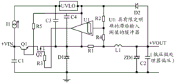
图6示出根据本公开的另一个示例性实施方式的开关式并联调节器电路。在该示例实施方式中,开关控制器为缓冲器U1。缓冲器U1具有联接至其输入端的分压器。分压器包括通过二极管D2联接在缓冲器U1的所述输入端和开关式并联调节器电路的输出端(+VOUT)之间的电阻器R2。分压器还包括联接在缓冲器U1的输入端和电感器L1之间的电阻器R3。缓冲器U1可具有限定明确的滞后缓冲输入阈值。例如,第一滞后缓冲输入阈值可约为3V,第二滞后缓冲输入阈值可约为2V。电阻器R2和电阻器R3的值可如此选择,使得在开关式并联调节器电路初始化时,当没有电流在电感器L1和电流感测电阻器R1中流动时,缓冲器输入电压高于3V。6 illustrates a switched shunt regulator circuit according to another exemplary embodiment of the present disclosure. In this example embodiment, the switch controller is buffer U1. Buffer U1 has a voltage divider coupled to its input. The voltage divider includes a resistor R2 coupled through diode D2 between the input of buffer U1 and the output (+VOUT) of the switched shunt regulator circuit. The voltage divider also includes a resistor R3 coupled between the input of the buffer U1 and the inductor L1. Buffer U1 may have a well-defined hysteresis buffer input threshold. For example, the first hysteresis buffer input threshold may be approximately 3V and the second hysteresis buffer input threshold may be approximately 2V. The values of resistor R2 and resistor R3 can be chosen such that upon initialization of the switched shunt regulator circuit, the buffer input voltage is above 3V when no current is flowing in inductor L1 and current sense resistor R1.
一旦在缓冲器U1的高压侧获得偏置电压,由于起始缓冲器输入电压大于3V,故缓冲器输出高信号以接通开关S1。当开关S1接通时,电流开始在电阻器R1和电感器L1中线性增加。在通过电感器L1的电流增加的同时,在电阻器R1和电阻器R3之间的节点的电压开始下降,在缓冲器U1的输入端的电压线性降低。在预定的电感器电流下,在缓冲器U1的输入端的电压达到第二滞后缓冲输入阈值,缓冲器输出低信号以关掉开关S1。电感器电流于是朝着接地下降,电流续流通过二极管D1。在电感器L1和电阻器R1中的电流从其峰值向零下降。第一滞后缓冲输入阈值被如此选择,使得一旦通过电感器L1的电流下降至预定的低电平,则缓冲器输出将变高以接通开关。预定的低电平优选约为零。在开关式并联调节器电路的运行期间,可连续重复该循环。Once the bias voltage is obtained on the high side of buffer U1, since the initial buffer input voltage is greater than 3V, the buffer outputs a high signal to turn on switch S1. When switch S1 is turned on, the current begins to increase linearly in resistor R1 and inductor L1. At the same time as the current through inductor L1 increases, the voltage at the node between resistor R1 and resistor R3 begins to drop, and the voltage at the input of buffer U1 decreases linearly. At a predetermined inductor current, the voltage at the input of buffer U1 reaches a second hysteretic buffer input threshold, and the buffer outputs a low signal to turn off switch S1. The inductor current then drops towards ground and the current freewheels through diode D1. The current in inductor L1 and resistor R1 drops from its peak value towards zero. The first hysteretic buffer input threshold is chosen such that once the current through inductor L1 drops to a predetermined low level, the buffer output will go high to turn on the switch. The predetermined low level is preferably about zero. This cycle can be repeated continuously during operation of the switched shunt regulator circuit.
有时优选开关式并联调节器的边界模式操作。如果电感器电流的预定的低水平约为零,则可在开关式并联调节器电路中发生边界模式操作。尽管电感器电流的优选的下限阈值约为零,但是如果电感器电流的下限阈值稍微高于零,则仍可进行边界模式操作。在边界模式操作期间的电流的波形(图5所示)具有从零至电感器峰值电流的三角形。无论开关式并联调节器电路的输入电压和输出电压如何,在边界模式操作期间的平均电流为电流峰值的一半。如果电感器电流的下限阈值基本上高于零,可进行连续电流模式操作。如果电感器电流的下限阈值约为零,在电感器电流增加而超过大约零之前存在延迟,则可进行间断电流运行模式。Boundary mode operation of switched shunt regulators is sometimes preferred. If the predetermined low level of the inductor current is about zero, boundary mode operation can occur in a switched shunt regulator circuit. Although the preferred lower threshold for inductor current is about zero, boundary mode operation is still possible if the lower threshold for inductor current is slightly above zero. The waveform of the current during boundary mode operation (shown in Figure 5) has a triangle from zero to the peak inductor current. Regardless of the input and output voltages of the switched shunt regulator circuit, the average current during boundary mode operation is half the current peak value. Continuous current mode operation is possible if the lower threshold of the inductor current is substantially above zero. If the lower threshold of the inductor current is about zero, there is a delay before the inductor current increases beyond about zero, and the discontinuous current mode of operation can be performed.
在图6的实施方式中,在施加输入电压(+VIN)时,致使电流源I1通过电阻器R1、电感器L1、电容器C2和负载电路对高压侧偏置滤波电容器C3充电,直到电容器C3两端的电压达到欠压锁定(UVLO)电路的预定的高电平。一旦达到该阈值,偏置电源被施加于缓冲器,开关式并联调节器电路运行开始。线性调节器可用于为缓冲器U1和/或内部电路维持固定偏压。在两个不同的预定电平下,可接通和关掉电流源I1。并联齐纳二极管可被放置在电容器C3的两端以对偏置电压进行钳位。如果缓冲器的静态电流和开关S1的栅极电荷低,所需的偏置功率可由输入源生成,而没有降级。也可利用生成控制偏置功率的其他方法。In the embodiment of FIG. 6, when the input voltage (+VIN) is applied, current source I1 is caused to charge the high side bias filter capacitor C3 through resistor R1, inductor L1, capacitor C2 and the load circuit until capacitor C3 is two The voltage at the terminal reaches a predetermined high level of an under-voltage lockout (UVLO) circuit. Once this threshold is reached, bias power is applied to the buffer and operation of the switched shunt regulator circuit begins. A linear regulator can be used to maintain a fixed bias voltage for buffer U1 and/or internal circuitry. The current source I1 can be switched on and off at two different predetermined levels. A parallel Zener diode can be placed across capacitor C3 to clamp the bias voltage. If the quiescent current of the buffer and the gate charge of switch S1 are low, the required bias power can be generated by the input source without degradation. Other methods of generating controlled bias power may also be utilized.
在一些示例性实施方式中,由于控制电路和感测节点的布置,由栅极驱动和寄生电容充电引起的电流尖脉冲不会被感测到。因此,可以不需要前沿消隐。In some exemplary embodiments, current spikes caused by gate drive and parasitic capacitance charging are not sensed due to the arrangement of the control circuitry and sense nodes. Therefore, leading edge blanking may not be required.
在一些实施方式中,缓冲器可具有传播延迟和/或开关可具有关断延迟。在这些情况下,在达到关断阈值之后,电感器电流可继续上升,直到开关关断。在电感器中生成的额外电流在整个输入电压范围上不是恒定的。由于电感器中的电流增加速率在高输入电压下更高,因此,在高输入电压下电感器中生成的额外电流大于在低输入电压下电感器中生成的额外电流。这会引起在平均输出电流中出现误差,并且输出电流在整个输入电压范围上不会是恒定的。在某些实施方式中,电流的变化不会是非常大的,且能够是可接受的。在其他实施方式中,开关式并联调节器电路可被配置成确保在最低输入电压下可获得足够的电流,且在最高的输入电压下增加的电流电平可由并联电压调节器消除。In some implementations, the buffers may have propagation delays and/or the switches may have turn-off delays. In these cases, after the turn-off threshold is reached, the inductor current may continue to rise until the switch turns off. The extra current generated in the inductor is not constant over the entire input voltage range. Since the rate of current increase in the inductor is higher at high input voltages, the additional current generated in the inductor at high input voltage is greater than the additional current generated in the inductor at low input voltage. This causes errors in the average output current, and the output current will not be constant over the entire input voltage range. In some embodiments, the change in current will not be very large and can be acceptable. In other embodiments, the switched shunt regulator circuit can be configured to ensure that sufficient current is available at the lowest input voltage, and that the increased current level at the highest input voltage can be eliminated by the shunt voltage regulator.
在某些实施方式中,可实现输出电流的更加精确的控制。例如,开关式并联调节器电路可具有线路前馈,使得源于输入源的DC信号被添加至感测到的电流,以补偿传播延迟。在其他实施方式中,开关式并联调节器电路可具有电流调节回路,该电流调节回路对形成在电流感测电阻器中的信号求平均值,并将其与固定参考进行比较。产生的误差可被用来改变缓冲器的关闭阈值,以补偿传播延迟。In certain embodiments, more precise control of the output current may be achieved. For example, a switched shunt regulator circuit may have line feedforward such that a DC signal originating from the input source is added to the sensed current to compensate for propagation delays. In other embodiments, the switched shunt regulator circuit may have a current regulation loop that averages the signal developed in the current sense resistor and compares it to a fixed reference. The resulting error can be used to change the off threshold of the buffer to compensate for the propagation delay.
在某些示例实施方式中,可使用单个的MOSFET开关。然而,高压MOSFET(>300V)可具有更高的栅极阈值,并且可需要5V或更高的驱动电压。电流源可被配置成利用在输出端的电压作为偏置电源电压。由于当输出电压被设定为约3.3V时,在续流期间,用于开关的偏置功率可源于输出端,故高压MOSFET会不适合用作开关。In some example embodiments, a single MOSFET switch may be used. However, high voltage MOSFETs (>300V) may have higher gate thresholds and may require drive voltages of 5V or higher. The current source may be configured to utilize the voltage at the output as a bias supply voltage. Since the bias power for switching can originate from the output during freewheeling when the output voltage is set to about 3.3V, high voltage MOSFETs may not be suitable for switching.
图7示出根据本公开的另一个示例性实施方式的开关式并联调节器电路。如图7所示,开关式并联调节器电路可包括发射极开关的双极晶体管开关(例如,共源共栅),该开关具有与低压MOSFET Q2串联的BJT Q1。BJT Q1由取自通过电阻器R5的偏置电源的固定电流来驱动,而MOSFET Q2为由缓冲器U1的输出端驱动的控制开关。共源共栅开关可具有对于BJT Q1的非常快的运行和提高安全运行区域。与其他共发射极配置相比,共源共栅开关还可为BJT Q1提供较低的存储时间和延迟。由于BJT Q1为电流驱动装置,故其可以在下至非常低的电压下(诸如,大约2.5V至3.3V)运行。控制MOSFET Q2可具有低的额定电压和大约1V至2V的低的栅极阈值。因此,共源共栅开关可在3.3V偏压下运行。某些示例实施方式可使用非常低的功率和电流,且可使用非常低的电流额定的BJT。某些600V额定的BJT会比相当的600V MOSFET在成本上显著降低。7 illustrates a switched shunt regulator circuit according to another exemplary embodiment of the present disclosure. As shown in FIG. 7, the switched shunt regulator circuit may include an emitter switched bipolar transistor switch (eg, cascode) with a BJT Q1 in series with a low voltage MOSFET Q2. BJT Q1 is driven by a fixed current drawn from the bias supply through resistor R5, while MOSFET Q2 is a control switch driven by the output of buffer U1. The cascode switch can have very fast operation and improved safe operating area for the BJT Q1. Cascode switches also provide lower storage time and latency for BJT Q1 compared to other common-emitter configurations. Since BJT Q1 is a current drive device, it can operate down to very low voltages, such as about 2.5V to 3.3V. Control MOSFET Q2 may have a low voltage rating and a low gate threshold of about 1V to 2V. Therefore, the cascode switch can operate at 3.3V bias. Certain example embodiments may use very low power and current, and may use very low current rated BJTs. Some 600V rated BJTs will cost significantly less than comparable 600V MOSFETs.
图8示出根据本公开的另一个示例实施方式的开关式并联调节器电路。如图8所示,开关式并联调节器电路可包括集成电路。例如,开关式并联调节器电路可包括电感器、开关、缓冲器和电流传感器,至少开关和缓冲器被包括在集成电路中。在其他实施方式中,更多或更少的组件可被包括在集成电路中,或位于集成电路的外部。在该示例实施方式中,电感器L1、并联电压调节器ZD1、电流感测电阻器R1和滤波电容器(C1,C2,C3)在集成电路的外部,而缓冲器、二极管和开关在集成电路的内部。在开关式并联调节器电路中使用集成电路可减少开关式并联调节器电路的总的组件数。8 illustrates a switched shunt regulator circuit according to another example embodiment of the present disclosure. As shown in FIG. 8, the switched shunt regulator circuit may include an integrated circuit. For example, a switched shunt regulator circuit may include inductors, switches, snubbers and current sensors, at least the switches and snubbers being included in an integrated circuit. In other embodiments, more or fewer components may be included in the integrated circuit, or located external to the integrated circuit. In this example embodiment, inductor L1, shunt voltage regulator ZD1, current sense resistor R1 and filter capacitors (C1, C2, C3) are external to the integrated circuit, while buffers, diodes and switches are external to the integrated circuit internal. The use of integrated circuits in the switched shunt regulator circuit can reduce the overall component count of the switched shunt regulator circuit.
图9示出根据本公开的另一个示例实施方式的开关式并联调节器电路100。如图9所示,电流源102的输入端101可通过整流器116联接至公用电网电源。尽管图9中示出桥式整流器,但也可使用用于将AC公用电网电源输入电压转换成DC电压的其他适合的电路,例如,半波整流器、全波整流器等。在某些实施方式中,公用电网电源可以是115VAC、230VAC等。FIG. 9 illustrates a switched
图10示出根据本公开的另一个示例实施方式的开关式并联调节器电路100。如图10所示,电流源102的输出端103可被联接至数字控制器106。数字控制器106可以是任何适合的数字控制器,例如,微处理器、微控制器、数字信号处理器、集成电路芯片等。数字控制器106可以是用于开关模式电源的控制器。开关式并联调节器电路100可允许低功率微处理器由公用电网电源直接供电。开关式并联调节器电路100可以是数控开关电源的一部分,微处理器需要在其控制主功率转换器之前首先被供电。在其他实施方式中,开关式并联调节器电路100可以是任何适合的产品的一部分,该产品需要在控制运行之前首先被通电的控制器或微处理器,并且通过微处理器吸入的负载电流在其整个运行中可具有最小变化。例如,开关式并联调节器电路100可以是低功率数控离线电源、家用电器(例如,空调、电饭煲、洗碗机、微波炉、电度表、无线控制器、由公用AC输入运行的智能机等)的一部分。FIG. 10 illustrates a switched
在本公开的某些示例性实施方式中,开关式并联调节器电路可提供直接来自例如115VAC、230VAC等的公用电网电源的非隔离稳定的低的偏置电压(例如,3.3V)。开关式并联调节器电路能够在3.3V下仅生成约10mA。开关式并联调节器电路可采用高压侧开关操作,且可以不采用用于调节的光耦合器。开关式并联调节器电路可提供低输出电压纹波,且可允许微处理器采用输出偏置电压作为用于模数转换(ADC)的控制基准。开关式并联调节器电路能够提供3.3V的微处理器电源电压,而没有首先生成更高的电源电压(例如,5V、6V等),然后利用线性调节器。开关式并联调节器可被配置成在续流期间从开关式并联调节器的输出电压获得用于开关式并联调节器的偏压。In certain exemplary embodiments of the present disclosure, the switched shunt regulator circuit may provide a non-isolated regulated low bias voltage (eg, 3.3V) directly from a utility power supply, eg, 115VAC, 230VAC, etc. . The switched shunt regulator circuit is able to generate only about 10mA at 3.3V. Switched shunt regulator circuits may operate with high side switching and may not use optocouplers for regulation. The switched shunt regulator circuit provides low output voltage ripple and allows the microprocessor to use the output bias voltage as a control reference for analog-to-digital conversion (ADC). A switched shunt regulator circuit can provide a microprocessor supply voltage of 3.3V without first generating a higher supply voltage (eg, 5V, 6V, etc.) and then utilizing a linear regulator. The switched shunt regulator may be configured to obtain a bias voltage for the switched shunt regulator from the output voltage of the switched shunt regulator during freewheeling.
图11示出根据本公开的另一个示例实施方式的开关式并联调节器电路。如图11所示,电流源的输出端可联接至非隔离式发光二极管(LED)驱动器电路。电流源可联接至离线LED驱动器,以在恒定电流下驱动LED。当电流源的输出端联接至LED驱动器时,LED可充当非精密的并联调节器,LED的正向电压降作为输出电压。11 illustrates a switched shunt regulator circuit according to another example embodiment of the present disclosure. As shown in Figure 11, the output of the current source can be coupled to a non-isolated light emitting diode (LED) driver circuit. A current source can be coupled to an offline LED driver to drive the LEDs at constant current. When the output of the current source is connected to the LED driver, the LED can act as a non-precision shunt regulator, with the forward voltage drop of the LED as the output voltage.
开关式并联调节器可被配置成初始化数字控制器,而不需要辅助功率转换器。开关式并联调节器电路可通过消除模拟辅助功率转换器PWM控制器而被用在完全数控电源中。在初始化时,数字控制器能够充分控制辅助转换器、以及其他功率转换块(例如,PFC转换器和DC/DC转换器)。开关式并联调节器电路的一部分可在集成电路中实施。在某些示例实施方式中,滞后操作可通过感测通过电感器的峰值电流和谷值电流来实现。在其他示例实施方式中,共源共栅开关可用于低压操作。The switched shunt regulator can be configured to initialize the digital controller without the need for an auxiliary power converter. Switched shunt regulator circuits can be used in fully digitally controlled power supplies by eliminating the analog auxiliary power converter PWM controller. At initialization, the digital controller is able to fully control the auxiliary converter, as well as other power conversion blocks (eg, PFC converter and DC/DC converter). A portion of the switched shunt regulator circuit may be implemented in an integrated circuit. In certain example embodiments, hysteretic operation may be achieved by sensing peak and valley currents through the inductor. In other example embodiments, cascode switches may be used for low voltage operation.
在某些示例实施方式中,开关式并联调节器可包括发射极开关的双极晶体管(ESBT)作为控制开关。利用ESBT作为控制开关可允许更快的运行(例如,堪比MOSFET),同时允许从低压输出(例如,3.3V的输出电压等)获得运行偏置电压。In certain example embodiments, a switched shunt regulator may include an emitter switched bipolar transistor (ESBT) as a control switch. Utilizing an ESBT as a control switch allows faster operation (eg, comparable to a MOSFET) while allowing the operating bias voltage to be obtained from a low voltage output (eg, an output voltage of 3.3V, etc.).
正如应该是显而易见的,任何示例实施方式的任何特征可与任何其他示例实施方式的一个或多个特征结合,而不脱离本公开的范围。As should be apparent, any feature of any example embodiment may be combined with one or more features of any other example embodiment without departing from the scope of this disclosure.
实施方式的前述描述已被提出用于说明和描述的目的。其不意在是详尽的或限制本公开。特定实施方式的单独的元件或特征通常不受限于该特定实施方式,但是,在适用情况下,单独的元件或特征是可互换的,且可用在所选的实施方式中,即使未特别示出或描述。该单独的元件或特征也可以许多方式变化。这种变化不被看成是脱离本公开,并且所有的这种变型意在被包括在本公开的范围内。The foregoing descriptions of embodiments have been presented for purposes of illustration and description. It is not intended to be exhaustive or to limit the present disclosure. Individual elements or features of a particular embodiment are generally not limited to that particular embodiment, but, where applicable, individual elements or features are interchangeable and can be used in a selected embodiment, even if not specifically show or describe. The individual elements or features can also vary in many ways. Such variations are not considered to be a departure from this disclosure, and all such variations are intended to be included within the scope of this disclosure.
Claims (24)
Applications Claiming Priority (3)
| Application Number | Priority Date | Filing Date | Title |
|---|---|---|---|
| US201361913053P | 2013-12-06 | 2013-12-06 | |
| US61/913,053 | 2013-12-06 | ||
| CN201410742865.5A CN104967294A (en) | 2013-12-06 | 2014-12-08 | Switching Parallel Regulator Circuit |
Related Parent Applications (1)
| Application Number | Title | Priority Date | Filing Date |
|---|---|---|---|
| CN201410742865.5A Division CN104967294A (en) | 2013-12-06 | 2014-12-08 | Switching Parallel Regulator Circuit |
Publications (1)
| Publication Number | Publication Date |
|---|---|
| CN112134458A true CN112134458A (en) | 2020-12-25 |
Family
ID=53272180
Family Applications (3)
| Application Number | Title | Priority Date | Filing Date |
|---|---|---|---|
| CN201410742865.5A Pending CN104967294A (en) | 2013-12-06 | 2014-12-08 | Switching Parallel Regulator Circuit |
| CN202010850845.5A Pending CN112134458A (en) | 2013-12-06 | 2014-12-08 | Switched parallel regulator circuit |
| CN201420766729.5U Expired - Fee Related CN204597768U (en) | 2013-12-06 | 2014-12-08 | Switched parallel regulator circuit |
Family Applications Before (1)
| Application Number | Title | Priority Date | Filing Date |
|---|---|---|---|
| CN201410742865.5A Pending CN104967294A (en) | 2013-12-06 | 2014-12-08 | Switching Parallel Regulator Circuit |
Family Applications After (1)
| Application Number | Title | Priority Date | Filing Date |
|---|---|---|---|
| CN201420766729.5U Expired - Fee Related CN204597768U (en) | 2013-12-06 | 2014-12-08 | Switched parallel regulator circuit |
Country Status (2)
| Country | Link |
|---|---|
| US (1) | US10014771B2 (en) |
| CN (3) | CN104967294A (en) |
Families Citing this family (10)
| Publication number | Priority date | Publication date | Assignee | Title |
|---|---|---|---|---|
| DE102012112391B4 (en) * | 2012-12-17 | 2018-10-04 | Phoenix Contact Gmbh & Co. Kg | Switching power supply with a cascode circuit |
| US9571091B2 (en) * | 2013-12-06 | 2017-02-14 | Astec International Limited | Methods for overdriving a base current of an emitter switched bipolar junction transistor and corresponding circuits |
| US10097192B2 (en) * | 2016-12-12 | 2018-10-09 | Mediatek Inc. | Circuits for current recycling and related methods |
| CN106787833B (en) * | 2016-12-13 | 2023-08-29 | 浙江恒业电子股份有限公司 | Power supply circuit with DC/DC conversion module |
| US10396654B2 (en) | 2017-10-25 | 2019-08-27 | Schneider Electric Solar Inverters Usa, Inc. | Start-up circuit |
| FR3083037A1 (en) | 2018-06-25 | 2019-12-27 | Commissariat A L'energie Atomique Et Aux Energies Alternatives | VOLTAGE REDUCER CONVERTER |
| US10707761B1 (en) * | 2019-04-25 | 2020-07-07 | Apple Inc. | Power converter with on-resistance compensation |
| US10784767B1 (en) * | 2019-05-30 | 2020-09-22 | Astec International Limited | Switching power converters with adaptively triggered analog-to-digital converters |
| US10778080B1 (en) * | 2019-06-06 | 2020-09-15 | Microchip Technology Incorporated | Self-biased non-isolated low-power switching regulator |
| CN116301162A (en) * | 2023-03-31 | 2023-06-23 | 浙江工业大学 | A Compatible Sampling Shunt Regulator Suitable for Loop Current Source |
Citations (8)
| Publication number | Priority date | Publication date | Assignee | Title |
|---|---|---|---|---|
| US5418707A (en) * | 1992-04-13 | 1995-05-23 | The United States Of America As Represented By The United States Department Of Energy | High voltage dc-dc converter with dynamic voltage regulation and decoupling during load-generated arcs |
| US6184667B1 (en) * | 1997-09-09 | 2001-02-06 | James Christopher Lacey | DC/DC converter |
| US6271651B1 (en) * | 2000-04-20 | 2001-08-07 | Volterra Semiconductor Corporation | Inductor shorting switch for a switching voltage regulator |
| CN101379887A (en) * | 2005-12-20 | 2009-03-04 | Tir科技公司 | Method and apparatus for controlling current supplied to electronic devices |
| US20090256535A1 (en) * | 2008-04-10 | 2009-10-15 | Intersil Americas Inc. | Varying operation of a voltage regulator, and components thereof, based upon load conditions |
| US20110156680A1 (en) * | 2009-12-25 | 2011-06-30 | Wen-Chung Yeh | Methods and related controllers for controlling output power of a power supply |
| CN102714462A (en) * | 2009-07-22 | 2012-10-03 | 沃福森微电子股份有限公司 | Improvements relating to DC-DC converters |
| US20130187619A1 (en) * | 2012-01-19 | 2013-07-25 | Fairchild Semiconductor Corporation | Shunt regulator |
Family Cites Families (6)
| Publication number | Priority date | Publication date | Assignee | Title |
|---|---|---|---|---|
| US5780999A (en) * | 1996-08-23 | 1998-07-14 | Laser Technology, Inc. | Voltage conversion circuit for a laser based distance measurement and ranging instrument |
| JP5268615B2 (en) * | 2008-12-15 | 2013-08-21 | キヤノン株式会社 | Power supply device and image forming apparatus |
| US8305004B2 (en) | 2009-06-09 | 2012-11-06 | Stmicroelectronics, Inc. | Apparatus and method for constant power offline LED driver |
| US8400123B2 (en) * | 2010-06-28 | 2013-03-19 | Infineon Technologies Austria Ag | Voltage converter and voltage conversion method |
| US9627966B2 (en) | 2012-04-05 | 2017-04-18 | Infineon Technologies Americas Corp. | Power converter having an advanced control IC |
| US9287798B2 (en) * | 2012-12-06 | 2016-03-15 | Stmicroelectronics, Inc. | High power factor primary regulated offline LED driver |
-
2014
- 2014-12-03 US US14/559,329 patent/US10014771B2/en not_active Expired - Fee Related
- 2014-12-08 CN CN201410742865.5A patent/CN104967294A/en active Pending
- 2014-12-08 CN CN202010850845.5A patent/CN112134458A/en active Pending
- 2014-12-08 CN CN201420766729.5U patent/CN204597768U/en not_active Expired - Fee Related
Patent Citations (8)
| Publication number | Priority date | Publication date | Assignee | Title |
|---|---|---|---|---|
| US5418707A (en) * | 1992-04-13 | 1995-05-23 | The United States Of America As Represented By The United States Department Of Energy | High voltage dc-dc converter with dynamic voltage regulation and decoupling during load-generated arcs |
| US6184667B1 (en) * | 1997-09-09 | 2001-02-06 | James Christopher Lacey | DC/DC converter |
| US6271651B1 (en) * | 2000-04-20 | 2001-08-07 | Volterra Semiconductor Corporation | Inductor shorting switch for a switching voltage regulator |
| CN101379887A (en) * | 2005-12-20 | 2009-03-04 | Tir科技公司 | Method and apparatus for controlling current supplied to electronic devices |
| US20090256535A1 (en) * | 2008-04-10 | 2009-10-15 | Intersil Americas Inc. | Varying operation of a voltage regulator, and components thereof, based upon load conditions |
| CN102714462A (en) * | 2009-07-22 | 2012-10-03 | 沃福森微电子股份有限公司 | Improvements relating to DC-DC converters |
| US20110156680A1 (en) * | 2009-12-25 | 2011-06-30 | Wen-Chung Yeh | Methods and related controllers for controlling output power of a power supply |
| US20130187619A1 (en) * | 2012-01-19 | 2013-07-25 | Fairchild Semiconductor Corporation | Shunt regulator |
Also Published As
| Publication number | Publication date |
|---|---|
| US10014771B2 (en) | 2018-07-03 |
| US20150162833A1 (en) | 2015-06-11 |
| CN204597768U (en) | 2015-08-26 |
| CN104967294A (en) | 2015-10-07 |
Similar Documents
| Publication | Publication Date | Title |
|---|---|---|
| CN204597768U (en) | Switched parallel regulator circuit | |
| US9742264B2 (en) | Boost inductor demagnetization detection for bridgeless boost PFC converter operating in boundary-conduction mode | |
| CN105322817B (en) | Single stage power conversion and adjusting for wireless charging system | |
| CN102832836B (en) | Cascade boost and inverting buck converter with independent control | |
| TWI501533B (en) | An off-line voltage regulator, off-line regulator integrated circuit and voltage convert method thereof | |
| CN106533209B (en) | Hybrid boost-bypass converter in two-stage converter and power converter | |
| US9241381B2 (en) | LED driving circuit, control circuit and associated current sensing circuit | |
| US20180007751A1 (en) | Control method and device employing primary side regulation in a quasi-resonant ac/dc flyback converter without analog divider and line-sensing | |
| US9131568B2 (en) | Light-emitting diode driving apparatus and semiconductor device | |
| CN115411927A (en) | Autonomous mode transition for multi-mode operation in a boost power factor correction converter | |
| CN104980021A (en) | System And Method For A Switched-mode Power Supply | |
| CN102130613B (en) | A power converter with a switch connected between the windings | |
| CN103229401A (en) | AC/DC power conversion method and apparatus | |
| KR102129872B1 (en) | Power converter using bi-directional active rectifying bridge | |
| TW201236347A (en) | Direct current/direct current converter, and power supply apparatus and electronic device using the same | |
| CN111033992A (en) | Digital Control of Switching Boundary Mode PFC Power Converters for Constant Crossover Frequency | |
| TW200934045A (en) | High efficiency charging circuit and power supplying system | |
| US11606037B2 (en) | Detection circuit and switching converter | |
| US20120014149A1 (en) | Power conversion apparatus and method | |
| US8541957B2 (en) | Power converter having a feedback circuit for constant loads | |
| US11258353B2 (en) | Power converter | |
| US8796950B2 (en) | Feedback circuit for non-isolated power converter | |
| US9369050B1 (en) | Indirect current sensing method for a constant current flyback converter | |
| US11557982B2 (en) | AC/DC power converters including current transformers for bidirectional current sensing | |
| JP2011083049A (en) | Voltage converter |
Legal Events
| Date | Code | Title | Description |
|---|---|---|---|
| PB01 | Publication | ||
| PB01 | Publication | ||
| SE01 | Entry into force of request for substantive examination | ||
| SE01 | Entry into force of request for substantive examination | ||
| WD01 | Invention patent application deemed withdrawn after publication |
Application publication date: 20201225 |
|
| WD01 | Invention patent application deemed withdrawn after publication |