Disclosure of Invention
In view of the above-mentioned shortcomings of the prior art, an object of the present invention is to provide a high-integration multi-antenna group and an antenna group module thereof, which are used to solve the problems that in the prior art, as many antennas as possible need to be placed in a smaller and smaller space, and the number of antennas placed in a limited space and the isolation between the antennas are difficult to be considered, thereby affecting the high integration and miniaturization development of electronic products.
To achieve the above and other related objects, the present invention provides a high-integration multi-antenna group, including at least:
the excitation unit comprises a slot excitation source and a slot excitation component, wherein the slot excitation source is loaded on the slot excitation component and excites the radiation slot to form a slot antenna;
the first dipole antenna is arranged in the radiation gap and comprises a first excitation source and a first antenna wire, and the first antenna wire is arranged along the direction of an included angle between-10 degrees and 10 degrees with the long edge of the radiation gap.
Optionally, the metal ground comprises a PCB board, an FPC board, a metal housing or a conductive metal coating.
Optionally, the excitation mode of the excitation unit is direct excitation or coupled excitation.
Optionally, the excitation mode of the excitation unit is that a dipole unit is coupled and fed, and a balun structure is introduced on the dipole.
Optionally, the excitation mode of the excitation unit is a direct excitation mode, the slot excitation component is bridged over the metal ground along the narrow side direction of the radiation slot, and the slot excitation source and the first dipole antenna are respectively and symmetrically distributed on two sides of a connecting line of center points of two narrow sides of the radiation slot; or the excitation mode of the excitation unit is a coupling excitation mode of a dipole unit, and the dipole unit and the first dipole antenna are respectively and symmetrically distributed on two sides of a connecting line of central points of two narrow sides of the radiation slot.
Optionally, the excitation mode of the first dipole antenna is direct excitation, and the first excitation source is directly loaded on the first antenna trace to form the dipole antenna.
Optionally, an excitation manner of the first dipole antenna is coupling excitation, the first dipole antenna includes a first excitation source, a first excitation component connected to the first excitation source, and a first antenna trace, the first excitation source is loaded on the first excitation component, and the first excitation component couples and excites the first antenna trace by virtue of a constraint effect of the radiation gap on an electromagnetic field, so that the first antenna trace operates in a dipole antenna mode.
Optionally, the slot excitation component and the first antenna trace are located on different spatial layers, and a spatial projection of the slot excitation component and the first antenna trace partially or completely overlaps.
Optionally, the excitation manner of the excitation unit is coupled excitation, the slot excitation component includes a first slot excitation component and a second slot excitation component connected to the slot excitation source, the first slot excitation component and the second slot excitation component are located in different spatial layers, and the slot excitation source is loaded on the first slot excitation component, so that the first slot excitation component performs coupled excitation on the second slot excitation component.
Optionally, the radiation gap is a closed gap surrounded by four sides of the metal ground or an open gap surrounded by four sides of the metal ground, and an opening of the open gap is located at a narrow side of the open gap.
Optionally, the multi-antenna group further includes: and the second dipole antenna is arranged in the radiation gap and comprises a second excitation source and a second antenna wire, and the second antenna wire is arranged along the direction of an included angle between-10 degrees and 10 degrees with the long edge of the radiation gap.
Optionally, the excitation mode of the excitation unit is a direct excitation mode, the slot excitation component is bridged over the metal ground along the narrow side direction of the radiation slot, and the slot excitation source, the first dipole antenna and the second dipole antenna are respectively and symmetrically distributed on two sides of a connecting line of central points of two narrow sides of the radiation slot; or the excitation mode of the excitation unit is a coupling excitation mode of a dipole unit, and the dipole unit, the first dipole antenna and the second dipole antenna are respectively and symmetrically distributed on two sides of a connecting line of central points of two narrow sides of the radiation slot.
Optionally, the excitation manner of the second dipole antenna is coupling excitation, the second dipole antenna further includes a second excitation component connected to the second excitation source, the second excitation source is loaded on the second excitation component, and the second excitation component couples and excites the second antenna trace by virtue of a constraint effect of the radiation gap on an electromagnetic field, so that the second antenna trace operates in a dipole antenna mode.
Optionally, the first antenna trace of the first dipole antenna and/or the second antenna trace of the second dipole antenna are used as an inductive stub of a distance sensor.
Optionally, the distance sensor is integrated on the slot excitation component or on the first antenna trace of the first dipole antenna or on the second antenna trace of the second dipole antenna, and a high-frequency filter structure is disposed therebetween.
Optionally, the slot driver is a WWAN driver, a MIMO driver, a WLAN driver, or a Sub 6G driver, the first driver is a MIMO driver, a WLAN driver, or a Sub 6G driver, and the second driver is a MIMO driver, a WLAN driver, or a Sub 6G driver.
The invention also provides an antenna group module, which comprises more than two high-integration multi-antenna groups.
As described above, according to the high-integration multi-antenna group and the antenna group module thereof of the present invention, a plurality of antenna groups (for example, a slot antenna and a first dipole antenna) are excited based on the same radiation slot in the slot antenna, and according to the size of the radiation slot, the present invention can be applied to antenna designs such as 2G, 3G, 4G, 5G, BT, Wi-Fi, Navigation, and UWB, and according to practical applications, the antenna routing can be integrated with a distance sensor, thereby realizing dual functions or spatial multiplexing, and further improving the integration of an antenna system; meanwhile, an electric field generated by the first dipole antenna is perpendicular to an electric field generated by the radiation gap, so that high isolation between the two antennas can be realized, and the isolation between the antennas is considered while the integration level of the antennas is improved.
Drawings
Fig. 1 to 4 are schematic diagrams illustrating the operation of a conventional slot antenna.
Fig. 5 and 6 are schematic diagrams showing the layout of the radiation slots in the high-integration multi-antenna group on the metal ground.
Fig. 7 to 10 show the two-antenna system of the multi-antenna set with high integration degree of the present invention, in which the first dipole antenna is excited by direct excitation.
Fig. 11 to 15 show the two-antenna system with high-integration multi-antenna group according to the present invention, wherein the excitation mode of the first dipole antenna is coupled excitation, and fig. 12 shows the spatial structure distribution diagram of the two antennas in the dashed box a of fig. 15.
Fig. 16 shows a two-antenna system with high-integration multi-antenna set according to the present invention, in which the excitation mode of the first dipole antenna and the excitation mode of the slot antenna excitation unit are both coupled excitation.
Fig. 17 shows a three-antenna system with high-integration multi-antenna set according to the present invention, in which the excitation mode of the first dipole antenna and the excitation mode of the second dipole antenna are both coupled excitation, and the excitation mode of the slot antenna is direct excitation.
Fig. 18 is a schematic structural diagram of a two-antenna system with multiple antenna groups with high integration level according to embodiment 1 of the present invention.
Fig. 19 and 20 show graphs of simulation S-parameters (isolation and return loss) and simulation efficiency of example 1.
Fig. 17 and fig. 21 are schematic structural diagrams of a three-antenna system with high-integration multi-antenna group according to embodiment 2 of the present invention, wherein fig. 21 is a schematic structural distribution diagram of the three antennas in fig. 17.
Fig. 22 to 24 are graphs showing the simulated return loss parameter, the simulated isolation parameter, and the simulated efficiency of example 2.
Fig. 25 to 27 show a measured return loss parameter map, a measured isolation parameter map, and a measured efficiency map of example 2.
Fig. 28 is a schematic diagram illustrating an application of a conventional distance sensor and antenna.
Fig. 29 is a schematic diagram illustrating an application of the antenna trace of the antenna in the high-integration multi-antenna group having the function of a distance sensor according to the present invention.
Fig. 30 is a schematic diagram illustrating an application of the present invention in which antennas and a distance sensor control circuit in a high-integration multi-antenna group are integrated to implement spatial multiplexing.
Fig. 31 is a schematic structural diagram of an antenna group module formed based on a high-integration antenna group in embodiment 3, which is applied to a notebook.
Fig. 32 to 36 are graphs showing the simulated return loss parameter, the simulated isolation parameter, and the simulated efficiency of example 3.
Fig. 37 is a schematic diagram illustrating an application of the high-integration antenna group of embodiment 4 to WWAN, MIMO, WLAN antenna design.
Fig. 38 to 41 are graphs showing the simulated return loss parameter, the simulated isolation parameter, and the simulated efficiency of example 4.
Description of the element reference numerals
10 metal ground
11 radiation slit
12 excitation unit
13 gap excitation source
14 gap excitation part
140 first gap excitation member
141 second gap excitation member
15 first dipole antenna
16 first excitation source
17 first excitation member
18 first antenna trace
19 second dipole antenna
20 second excitation source
21 second excitation member
22 second antenna trace
24 distance sensor control circuit
25 insulating dielectric layer
26 Metal rotating shaft
27 upper half piece
28 lower half
29 electric connection structure
30 capacitance
31 inductance
32 antenna trace
33 distance sensor signal line
34 first antenna group
35 second antenna group
36 third antenna group
37 antenna ground
A dotted line frame
Detailed Description
The embodiments of the present invention are described below with reference to specific embodiments, and other advantages and effects of the present invention will be easily understood by those skilled in the art from the disclosure of the present specification. The invention is capable of other and different embodiments and of being practiced or of being carried out in various ways, and its several details are capable of modification in various respects, all without departing from the spirit and scope of the present invention.
Please refer to fig. 1 to 41. It should be noted that the drawings provided in the present embodiment are only for illustrating the basic idea of the present invention, and the drawings only show the components related to the present invention rather than being drawn according to the number, shape and size of the components in actual implementation, and the type, quantity and proportion of each component in actual implementation may be changed arbitrarily, and the layout of the components may be more complicated. The shape of the radiating slot of the slot antenna in this embodiment is also rectangular as a whole, but it is possible to allow the long and/or short sides of the radiating slot to have some small protrusions and/or recesses, but these small protrusions and/or recesses do not affect the horizontal orientation of the long sides and the vertical orientation of the short sides of the radiating slot as a whole. Also, the long and/or short sides of the antenna track in this embodiment may also have some small protrusions and/or recesses, but these small protrusions and/or recesses do not affect the horizontal orientation of the long sides and the vertical orientation of the short sides of the antenna track as a whole. The slot antenna is an antenna which is provided with a slot on a waveguide, a metal plate or a resonant cavity, and electromagnetic waves radiate to an external space through the slot, has the characteristics of low profile, easy conformation, simple processing and the like, and is widely applied to various electronic products. As shown in fig. 1 to 4, the slot antenna is a common slot antenna, and may be divided into a direct feed (as shown in fig. 1), a loop feed (as shown in fig. 2), a monopole coupled feed (as shown in fig. 3), and a dipole coupled feed (as shown in fig. 4) according to the form of the feed. With the development trend of high integration and miniaturization of electronic products, the integration level of the antenna is severely tested.
Based on the above, the invention provides an antenna system for forming a high-integration multi-antenna group based on the slot in the slot antenna, wherein a plurality of antennas are arranged in the limited slot space, and the isolation among the plurality of antennas is better, so that the antenna integration is improved.
Specifically, as shown in fig. 7, the high-integration multi-antenna group of the present invention at least includes:
the antenna comprises a metal ground 10, a radiation slot 11 and an excitation unit 12, wherein the radiation slot 11 is arranged on the metal ground 10, the excitation unit 12 comprises a slot excitation source 13 and a slot excitation component 14, and the slot excitation source 13 is loaded on the slot excitation component 14 and excites the radiation slot 11 to form a slot antenna.
The first dipole antenna 15 is disposed in the radiation slot 11, the first dipole antenna 15 includes a first excitation source 16 and a first antenna trace 18, the first antenna trace 18 is disposed along a long side of the radiation slot 11 at an included angle between-10 ° and 10 °, where it should be noted that the included angle includes a head-end point value, that is, the included angle includes that the first antenna trace 18 is disposed along a long side of the radiation slot 11 at an included angle between-10 ° and 10 °. So that the isolation between the first dipole antenna 15 and the slot antenna meets the working index.
Through exciting a plurality of antennas (for example, the slot antenna and the first dipole antenna) in the same radiation slot, antenna designs such as 2G, 3G, 4G, 5G, BT, Wi-Fi, Navigation and UWB can be applied according to the size of the radiation slot, so that the integration level of the antennas is improved, and meanwhile, the electric field generated by the first dipole antenna is perpendicular to the electric field generated by the radiation slot, so that high isolation between the two antennas is realized.
By way of example, the metal ground 10 may be in any form suitable for forming a slot antenna, such as a PCB board, an FPC board, a metal housing, a conductive metal coating, or the like, as long as it is sufficiently conductive. The metal ground 10 may be an integrally formed metal ground; it may also be a metal ground that is fixed in a detachable manner, for example, in the area of the hinge of a conventional reversible electronic device, the metal hinge 26, the upper and lower halves 27, 28 of the electronic device and the electrical connection structure 29 electrically connecting the upper and lower halves form the metal ground 10 with the radiation slot 11 (see fig. 18).
As shown in fig. 5 and 6, the radiation slot 11 may be a closed slot surrounded by four sides of the metal ground (as shown in fig. 5) or an open slot surrounded by four sides of the metal ground, and an opening of the open slot is located at a narrow side of the open slot.
As an example, the slot driver 13 may be a WWAN driver, a MIMO driver, a WLAN driver, or a Sub 6G driver, and the first driver 16 may be a MIMO driver, a WLAN driver, or a Sub 6G driver.
As shown in fig. 7 to 10, as an example, the excitation manner of the excitation unit 12 of the slot antenna may be a direct excitation manner, for example, the excitation manner of the excitation unit 12 in fig. 7 is a direct feeding excitation manner, and the excitation manner of the excitation unit 12 in fig. 9 is a loop feeding excitation manner; the excitation method of the excitation unit 12 of the slot antenna may be a coupling excitation method, for example, the excitation method of the excitation unit 12 in fig. 8 is a monopole coupling feed excitation method, and the excitation method of the excitation unit 12 in fig. 10 is a dipole coupling feed excitation method. Preferably, when the excitation mode of the excitation unit 12 is a direct feeding excitation mode, the slot excitation component 14 is bridged over the metal ground 10 along the narrow side direction of the radiation slot 11, and at this time, the slot excitation source 13 is disposed in the middle of the slot excitation component 14, that is, in the middle of the connection line of the central points of the two narrow sides of the radiation slot 11, and meanwhile, the first dipole antennas 15 are also symmetrically distributed on both sides of the connection line of the central points of the two narrow sides of the radiation slot, and at this time, the best isolation between the slot antennas and the first dipole antennas can be obtained. Because the slot excitation source 13 is located in the middle of the narrow side of the radiation slot 11, the electric field excited by the radiation slot 11 is spatially symmetrically distributed in the radiation slot region, and the first dipole antenna 15 is also located in the middle of the narrow side of the radiation slot, and the electric field excited by the first dipole antenna is also spatially symmetrically distributed in the radiation slot region, at this time, the spatial coupling between the two antennas can be minimized, so that the optimal isolation degree is achieved. In addition, the feeding coaxial line of the slot exciting source 13 can be wired along the slot exciting component 13, and the balance state of the vertical and orthogonal space electric field of the two antennas is ensured to the maximum extent. Similarly, when the excitation mode of the excitation unit 12 is a coupling excitation mode of a dipole unit, the dipole unit and the first dipole antenna 15 may also be symmetrically distributed on two sides of a connection line of central points of two narrow sides of the radiation slot, so as to reduce the spatial coupling degree between the two antennas to the maximum extent, thereby achieving the best isolation degree.
As an example, the excitation mode of the excitation unit 12 is a dipole unit coupling feeding, and a balun structure may be introduced on the dipole, so as to improve the stability of the antenna system.
As another example, as shown in fig. 16, the excitation mode of the excitation unit 12 is coupled excitation, the slot excitation member 14 includes a first slot excitation member 140 and a second slot excitation member 141 connected to the slot excitation source 13, the first slot excitation member 140 and the second slot excitation member 141 are located in different spatial layers, the slot excitation source 13 is applied to the first slot excitation member 140, and the first slot excitation member 140 couples and excites the second slot excitation member 141, so that the second slot excitation member 141 excites the radiation slot 11 to form the slot antenna.
As shown in fig. 7 to 10, as an example, the first dipole antenna 15 may be directly excited, where the first dipole antenna 15 includes a first excitation source 16 and a first antenna trace 18, and the first excitation source 16 is directly loaded on the first antenna trace 18 to form a dipole antenna.
As shown in fig. 11 to 15, as an example, the first dipole antenna 15 may be excited by coupling excitation, the first dipole antenna 15 comprises a first excitation source 16, a first excitation member 17 connected to the first excitation source 16 and a first antenna trace 18, the shape, size and spatial position of the first excitation member 17 and the first antenna trace 18 are not limited, as long as under the excitation of the first excitation source 16, the first excitation component 17 can generate coupling excitation to the first antenna trace 18, and the working principle is that the first excitation source 16 is loaded on the first excitation component 17, and the first excitation component 17 couples and excites the first antenna trace 18 by virtue of the constraint action of the radiation gap on the electromagnetic field, so that the first antenna trace 18 works in a dipole antenna mode. As shown in fig. 12, it is preferable that the spatial projection of the first excitation component 17 and the spatial projection of the first antenna trace 18 at least partially overlap, and at this time, the coupling effect of the first excitation component 17 to the first antenna trace 18 is better. The first dipole antenna 15 adopts a coupling excitation mode, so that the size of the first antenna wire 18 can be effectively reduced, and the miniaturization of the first dipole antenna is realized by adjusting the coupling area and the thickness of the insulating medium layer 25. As shown in fig. 11, the excitation method of the first dipole antenna 15 is coupling excitation, and the excitation method of the excitation unit 12 of the slot antenna is direct feeding excitation; as shown in fig. 13, the excitation method of the first dipole antenna 15 is coupling excitation, and the excitation method of the excitation unit 12 of the slot antenna is monopole coupling feeding excitation; as shown in fig. 14, the excitation mode of the first dipole antenna 15 is coupling excitation, and the excitation mode of the excitation unit 12 of the slot antenna is loop feed excitation; as shown in fig. 15, the excitation method of the first dipole antenna 15 is coupled excitation, and the excitation method of the excitation unit 12 of the slot antenna is dipole coupled feeding.
As an example, when the slot excitation component 14 of the excitation unit 12 and the first antenna trace 18 of the first dipole antenna 15 are located at different spatial layers, the spatial projection of the slot excitation component 14 and the first antenna trace 18 may partially or completely overlap, so that more space may be reserved for the radiation slot to provide other antennas, and a spatial condition is provided for further improving the antenna integration level. For example, as shown in fig. 11, the excitation manner of the excitation unit 12 of the slot antenna is direct feeding, and the excitation manner of the first dipole antenna 15 is coupling excitation, in this case, the slot excitation component 14 may be partially or completely overlapped with the spatial projection of the first antenna trace 18; as shown in fig. 15, the excitation manner of the excitation unit 12 of the slot antenna is dipole coupling feeding, the excitation manner of the first dipole antenna 15 is coupling excitation, and at this time, the slot excitation component 14 may be partially or completely overlapped with the spatial projection of the first antenna trace 18; for example, the excitation mode of the excitation unit 12 of the slot antenna is coupled excitation, the excitation mode of the first dipole antenna 15 is direct excitation, and the slot excitation component 14 may be partially or completely overlapped with the spatial projection of the first antenna trace 18. As long as the slot excitation member 14 and the first antenna trace 18 of the first dipole antenna 15 are located at different spatial layers, the spatial projection of the slot excitation member 14 and the first antenna trace 18 can be set to partially or completely overlap.
Here, as shown in fig. 12, when the antenna of the present invention has different spatial layer structures, the insulating medium layer 25 is disposed between two adjacent layers, so that the antenna has a spatial three-dimensional layered structure.
As shown in fig. 16, as an example, both the excitation method of the excitation unit 12 and the excitation method of the first dipole antenna 15 are coupled excitation, wherein the slot excitation member 14 includes a first slot excitation member 140 and a second slot excitation member 141 connected to the slot excitation source 13, the first slot excitation member 140 and the second slot excitation member 141 are located at different spatial layers, the slot excitation source 13 is applied to the first slot excitation member 140, and the first slot excitation member 140 couples and excites the second slot excitation member 141, so that the second slot excitation member 141 excites the radiation slot 11 to form the slot antenna; the first dipole antenna 15 includes a first excitation source 16, a first excitation component 17 electrically connected to the first excitation source 16, and a first antenna trace 18, where the first excitation component 17 and the first antenna trace 18 are located at different spatial layers, the first excitation source 16 is loaded on the first excitation component 17, and the first excitation component 17 couples and excites the first antenna trace 18 by means of the constraint action of the radiation gap on the electromagnetic field, so that the first antenna trace 18 operates in a dipole antenna mode.
As shown in fig. 17, as an example, in addition to the slot antenna 12 and the first dipole antenna 15, the multi-antenna group may further include a second dipole antenna 19 disposed in the radiation slot 11, where the second dipole antenna 19 includes a second excitation source 20 and a second antenna trace 22, and the second antenna trace 22 is disposed along a direction of an included angle between-10 ° and 10 ° with a long side of the radiation slot 11, where it should be noted that the included angle includes a head-end point value, that is, the included angle includes that the second antenna trace 22 is disposed along a direction of an included angle between-10 ° and 10 ° with a long side of the radiation slot 11, so that an isolation between the second dipole antenna 19 and the slot antenna meets an operation criterion.
As an example, the excitation manner of the second dipole antenna 19 may be direct excitation, where the second dipole antenna 19 includes a second excitation source 20 and a second antenna trace 22, and the second excitation source 20 is directly loaded on the second antenna trace 22 to form a dipole antenna.
As shown in fig. 17, as an example, the excitation manner of the second dipole antenna 19 may be coupling excitation, the second dipole antenna 19 includes a second excitation source 20, a second excitation component 21 connected to the second excitation source 20, and a second antenna trace 22, shapes, sizes, and spatial positions of the second excitation component 21 and the second antenna trace 22 are not limited, as long as the second excitation component 21 can generate coupling excitation on the second antenna trace 22 under excitation of the second excitation source 20, and an operation principle is that the second excitation source 20 is loaded on the second excitation component 21, and the second excitation component 21 couples and excites the second antenna trace 22 by virtue of a constraint effect of the radiation gap on an electromagnetic field, so that the second antenna trace 22 operates in a dipole antenna mode. Preferably, the spatial projections of the second excitation component 21 and the second antenna trace 22 are at least partially overlapped, and at this time, the coupling effect of the second excitation component 21 to the second antenna trace 22 is better.
As an example, the second excitation source 20 may be a MIMO excitation source, a WLAN excitation source, or a Sub 6G excitation source.
As shown in fig. 17, as an example, the excitation mode of the excitation unit 12 is a direct excitation mode, the slot excitation member 14 is bridged over the metal ground 10 along the narrow side direction of the radiation slot 11, and the slot excitation source 13, the first dipole antenna 15 and the second dipole antenna 19 are respectively and symmetrically distributed on two sides of a connection line of central points of two narrow sides of the radiation slot, so that spatial coupling between the three antennas can be minimized, and an optimal isolation degree can be achieved. Similarly, when the excitation mode of the excitation unit 12 is a coupling excitation mode of a dipole unit, the first dipole antenna 15 and the second dipole antenna 19 may also be symmetrically distributed on two sides of a central point connecting line of two narrow sides of the radiation slot, so as to reduce the spatial coupling degree between the three antennas to the maximum, thereby achieving the best isolation degree.
As shown in fig. 17, the first dipole antenna 15 and the second dipole antenna 19 are disposed at two ends along the long side of the radiation slot 11, for example, to improve the isolation between the first dipole antenna 15 and the second dipole antenna 19.
As an example, the first antenna trace 18 of the first dipole antenna 15 and/or the second antenna trace 22 of the second dipole antenna 19 are used as a sensing stub of the distance sensor 24, so as to realize dual functions of an antenna and a sensor, as shown in fig. 29, that is, both the first antenna trace 18 and the second antenna trace 22 are used as a sensing stub of the distance sensor 24. As shown in fig. 28, for an application diagram of a conventional distance sensor (P-sensor) and an antenna, generally, in the prior art, a completely floating distance sensor sensing stub does not have an antenna function, so in order to make an antenna trace 32 have good sensing sensitivity, a capacitor 30 needs to be connected to a feed point and a ground point of the antenna, so that the antenna is in a floating state at an operating frequency of the P-sensor, and a detection signal line of the distance sensor needs to be filtered at a high frequency when being connected to the antenna, which is generally implemented by connecting an inductor 31. In this example, as shown in fig. 29, the first antenna trace 18 and the second antenna trace 22 are both in a completely floating state, and the first antenna trace 18 and the second antenna trace 22 are used alone or together as a sensing stub of a distance sensor, so that the first antenna trace and the second antenna trace have dual effects of antenna and distance sensing.
As another example, the distance sensor 24 may be integrated on the slot excitation component 14 or the first antenna trace 18 of the first dipole antenna 15 or the second antenna trace 22 of the second dipole antenna 19, and only a high-frequency filtering structure (e.g., an inductor 31) is disposed between the two to reduce mutual interference of signals between the two, so as to further improve the integration level of the electronic product, as shown in fig. 30, that is, the control circuit area of the distance sensor 24 is integrated on the first antenna trace 18, so as to implement spatial multiplexing, thereby further improving the integration level of the antenna system.
It should be noted that the relative positions of the slot region 11, the excitation unit 12, the first dipole antenna 15 and the second dipole antenna 19 in the highly integrated antenna set can be adjusted according to actual requirements without departing from the design principle of the present invention. For a spatial multi-layer structure, the high-integration antenna group can be located in any one or more layers of the multi-layer structure.
The high-integration antenna group of the present invention will be described in detail with reference to the specific drawings and the corresponding embodiments, and it is obvious that the described embodiments are only a part of the embodiments of the present invention, not all of the embodiments. All other embodiments, which can be derived by a person skilled in the art from the embodiments of the present invention without making any creative effort, shall fall within the protection scope of the present invention.
Example 1
As shown in fig. 12 and 18, wherein fig. 12 is a schematic diagram of a spatial structure distribution of the slot antenna and the first dipole antenna in fig. 18, for a simplified notebook computer model, an upper half 27 and a lower half 28 of the notebook computer form an angle of 90 °, and since the processing methods of the metal shafts on both sides are the same, only the metal shaft 26 on one side is simulated in this embodiment. The high-integration antenna group is applied to a rotating shaft area (50mm × 15mm) of a notebook computer, the metal ground 10 is formed by an upper half 27, a lower half 28, a metal rotating shaft 26 and an electric connection structure 29 electrically connecting the upper half and the lower half of the notebook computer, the rotating shaft area in the metal ground forms the radiation slot 11, an excitation mode of an excitation unit 12 placed in the rotating shaft area is a dipole coupling feeding mode, a slot excitation source 13 of the excitation unit is an MIMO antenna signal source, the MIMO antenna signal source is loaded on a slot excitation component 14, so that the slot excitation component 14 excites the rotating shaft area to form the slot antenna, and the slot antenna is an MIMO antenna with an operating frequency range of 1700MHz to 6000 MHz. In addition, the excitation mode of the first dipole antenna 15 disposed in the rotating shaft region is coupling excitation, the first excitation source 16 of the first dipole antenna 15 is a WLAN antenna signal source, the WLAN antenna signal source is loaded on the first excitation part 17, the first excitation part 17 couples and excites the first antenna wire 18 by virtue of the constraint effect of the rotating shaft region on the electromagnetic field, so that the first antenna wire 18 operates in a dipole antenna mode, and the first dipole antenna is a WLAN antenna with a dual-frequency (2400 MHz-2500 MHz; 5150 MHz-5850 MHz) operating frequency band. And the slot excitation component 14 and the first antenna trace 18 are located at different spatial layers, and the spatial projections between the two overlap. The slot antenna is perpendicular to the working electric field of the first dipole antenna. The scheme utilizes the structural characteristics of the notebook computer, does not need additional antenna clearance and furthest ensures the integrity of ID design. Fig. 19 and 20 are a simulation S-parameter (isolation and return loss) graph and a simulation efficiency graph of the two antennas of the present embodiment, and it can be seen that the two antennas cover respective operating frequency bands, and the isolation is better than-25 dB. In the embodiment, the high-isolation dual-antenna design is realized in a narrow rotating shaft space, and a brand new scheme is provided for the notebook computer antenna design.
Example 2
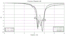
As shown in fig. 17 and 21, fig. 21 is a schematic diagram of the spatial structure distribution of the slot antenna, the first dipole antenna and the second dipole antenna in fig. 17. The working electric field of the slot antenna is respectively vertical and orthogonal to the working electric fields of the first dipole antenna and the second dipole antenna. In this embodiment, the size of the radiation slot 11 on the metal ground 10 is 60mm × 15mm × 2mm, the excitation mode of the excitation unit 12 disposed in the radiation slot 11 is a direct power feeding mode, the slot excitation source 13 of the excitation unit 12 is a MIMO antenna signal source, the MIMO antenna signal source is loaded on the slot excitation component 14, the slot excitation component 14 excites the radiation slot 11 to form the slot antenna, the slot antenna is a MIMO antenna with an operating frequency range of 1700MHz to 6000MHz, and the MIMO antenna signal source is located in the middle of the slot excitation component 14, so as to obtain the optimal isolation. In addition, the excitation mode of the first dipole antenna 15 disposed on the right side of the radiation slot 11 is coupling excitation, the first excitation source 16 of the first dipole antenna 15 is a WLAN antenna signal source, the WLAN antenna signal source is loaded on the first excitation part 17, the first excitation part 17 couples and excites the first antenna wire 18 by virtue of the constraint effect of the radiation slot 11 on the electromagnetic field, so that the first antenna wire 18 operates in a dipole antenna mode, and the first dipole antenna is a WLAN antenna with a dual-frequency (2400 MHz-2500 MHz; 5150 MHz-5850 MHz) operating frequency band. And the slot excitation component 14 and the first antenna trace 18 are located at different spatial layers, and the spatial projections between the two overlap. Furthermore, the excitation mode of the second dipole antenna 19 disposed on the left side of the radiation slot 11 is coupling excitation, the second excitation source 20 of the second dipole antenna 19 is a Sub-6G antenna signal source, the Sub-6G antenna signal source is loaded on the second excitation part 21, the second excitation part 21 couples and excites the second antenna trace 22 by virtue of the constraint effect of the radiation slot 11 on the electromagnetic field, so that the second antenna trace 22 operates in a dipole antenna mode, and the second dipole antenna is an antenna with an operating frequency band of 3300MHz to 3800 MHz. Fig. 22 to fig. 24 are a simulation return loss parameter diagram, a simulation isolation parameter diagram and a simulation efficiency diagram of the three antennas of the present embodiment, respectively, and it can be seen that the three antennas respectively cover respective working frequency bands, and the isolation between the three antennas is better than-25 dB. Fig. 25 to 27 are a measured return loss parameter diagram, a measured isolation parameter diagram, and a measured efficiency diagram of the three antennas of the present embodiment, respectively, and it can be seen that the measurement results are consistent with the simulation results.
Example 3
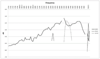
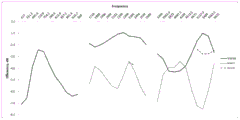
Fig. 31 shows a simplified notebook model with the top half 27 and bottom half 28 of the notebook at 90 deg.. The multi-antenna group structure in embodiment 2 is applied to the middle hinge area of a notebook computer, and an antenna group module formed by the high-integration multi-antenna group in embodiment 2 can be constructed, specifically, at least two high-integration multi-antenna groups in embodiment 2 can be integrated in the middle hinge area of the same notebook computer to form an antenna group module, as shown in fig. 31, three high-integration antenna groups in embodiment 2 are shown, which are a first antenna group 34, a second antenna group 35, and a third antenna group 36, respectively, and each antenna group has a size of 55mm x 10mm x 1.5mm, and includes three antennas (MIMO, WLAN, Sub 6G), so that a 9-antenna system can be designed in the middle hinge area. As shown in fig. 31, the excitation method of the excitation unit 12 disposed in the radiation slot 11 of the left first antenna group 34 is a direct feeding method, the slot excitation source 13 of the excitation unit 12 is a MIMO antenna signal source, the MIMO antenna signal source is loaded on the slot excitation component 14, so that the slot excitation component 14 excites the radiation slot 11 to form the slot antenna, the slot antenna is a MIMO antenna with an operating frequency range of 1700MHz to 6000MHz, and the MIMO antenna signal source is located in the middle of the slot excitation component 14 to obtain an optimal isolation. In addition, the excitation mode of the first dipole antenna 15 disposed on the left side of the radiation slot 11 is coupling excitation, the first excitation source 16 of the first dipole antenna 15 is a WLAN antenna signal source, the first dipole antenna is a WLAN antenna with a dual-frequency (2400 MHz-2500 MHz; 5150 MHz-5850 MHz) working frequency band, the excitation mode of the second dipole antenna 19 disposed on the right side of the radiation slot 11 is coupling excitation, the second excitation source 20 of the second dipole antenna 19 is a Sub-6G antenna signal source, and the second dipole antenna is an antenna with a working frequency band of 3300 MHz-3800 MHz. The structural layout of the second antenna group and the third antenna group is consistent with that of the first antenna group, and the description is not repeated here. Fig. 32 to 34 are graphs of simulated return loss parameters of the MIMO, WLAN, Sub 6G antenna of fig. 31. The isolation parameter for the poor part between the antennas is given in fig. 35, and it can be seen that the isolation between the antennas is better than-10 dB. Fig. 36 is a simulation result of the simulation efficiency diagram of three antennas in the first antenna group, which shows that the antenna performance meets the basic operation index.
Example 4
Fig. 37 shows an embodiment of the present invention applied to WWAN, MIMO, WLAN antenna design. In this embodiment, the size of the radiation slot 11 on the metal ground 10 is 120mm × 15mm × 2mm, the excitation method of the excitation unit 12 placed in the radiation slot 11 is a monopole coupling feeding method, the slot excitation source 13 of the excitation unit 12 is a WWAN antenna signal source, which is loaded on the slot excitation member 14, so that the slot excitation member 14 excites the radiation slot 11 to form the slot antenna, which is a WWAN antenna with an operating frequency band of 600MHz to 6000 MHz. In addition, the excitation mode of the first dipole antenna 15 disposed on the left side of the radiation slot 11 is coupling excitation, the first excitation source 16 of the first dipole antenna 15 is an MIMO antenna signal source, the MIMO antenna signal source is loaded on the first excitation component 17, the first excitation component 17 couples and excites the first antenna trace 18 by virtue of the constraint effect of the radiation slot 11 on the electromagnetic field, and the working frequency band of the first dipole antenna is 1700MHz to 6000 MHz. Moreover, the excitation mode of the second dipole antenna 19 disposed on the right side of the radiation slot 11 is coupling excitation, the second excitation source 20 of the second dipole antenna 19 is a WLAN antenna signal source loaded on the second excitation component 21, the second excitation component 21 couples and excites the second antenna trace 22 by virtue of the constraint effect of the radiation slot 11 on the electromagnetic field, and the second dipole antenna is a dual-frequency (2400 MHz-2500 MHz; 5150 MHz-5850 MHz) WLAN antenna. Fig. 38 to 41 are a simulation return loss parameter diagram, a simulation isolation parameter diagram, and a simulation efficiency diagram of the three antennas of this embodiment, respectively, and it can be seen that the three antennas cover respective working frequency bands, and the isolation between the three antennas is better than-10 dB, which basically meets the working index of the antennas. The gap in this embodiment may be a middle hinge area of the notebook computer or a window area above a keyboard of the notebook computer, which is not limited herein.
It should be noted that the 4 embodiments are only some of the designs of the present invention, and other combinations of the slot antenna, the first dipole antenna and the second dipole antenna can be applied to the embodiments. Different combination modes and different antenna isolation degrees can be selected preferably according to specific requirements. The performance and size of the antenna in the above 4 embodiments have the possibility of optimization, and can be further spread to working frequency bands of WiFi-6, UWB, and the like. Any optimization of the antenna using matching, switching, etc. is within the scope of the present invention.
In summary, the present invention provides a high-integration multi-antenna group and an antenna group module thereof, wherein a plurality of antenna groups (a slot antenna and a first dipole antenna) are excited based on a same radiation slot in a slot antenna, and according to the size of the radiation slot, the present invention is applicable to antenna designs such as 2G, 3G, 4G, 5G, BT, Wi-Fi, Navigation, and UWB, and according to practical applications, an antenna trace can be integrated with a distance sensor, thereby realizing dual functions or spatial multiplexing, and further improving the integration level of an antenna system; meanwhile, an electric field generated by the first dipole antenna is perpendicular to an electric field generated by the radiation gap, so that high isolation between the two antennas can be realized, and the isolation between the antennas is considered while the integration level of the antennas is improved. Therefore, the invention effectively overcomes various defects in the prior art and has high industrial utilization value.
The foregoing embodiments are merely illustrative of the principles and utilities of the present invention and are not intended to limit the invention. Any person skilled in the art can modify or change the above-mentioned embodiments without departing from the spirit and scope of the present invention. Accordingly, it is intended that all equivalent modifications or changes which can be made by those skilled in the art without departing from the spirit and technical spirit of the present invention be covered by the claims of the present invention.