CN111786659A - A wide-range high-precision charge pulse generating circuit and working method - Google Patents
A wide-range high-precision charge pulse generating circuit and working method Download PDFInfo
- Publication number
- CN111786659A CN111786659A CN202010576666.7A CN202010576666A CN111786659A CN 111786659 A CN111786659 A CN 111786659A CN 202010576666 A CN202010576666 A CN 202010576666A CN 111786659 A CN111786659 A CN 111786659A
- Authority
- CN
- China
- Prior art keywords
- pin
- switch
- normally open
- double
- control
- Prior art date
- Legal status (The legal status is an assumption and is not a legal conclusion. Google has not performed a legal analysis and makes no representation as to the accuracy of the status listed.)
- Pending
Links
Images
Classifications
-
- H—ELECTRICITY
- H03—ELECTRONIC CIRCUITRY
- H03K—PULSE TECHNIQUE
- H03K3/00—Circuits for generating electric pulses; Monostable, bistable or multistable circuits
- H03K3/01—Details
- H03K3/013—Modifications of generator to prevent operation by noise or interference
-
- G—PHYSICS
- G01—MEASURING; TESTING
- G01V—GEOPHYSICS; GRAVITATIONAL MEASUREMENTS; DETECTING MASSES OR OBJECTS; TAGS
- G01V5/00—Prospecting or detecting by the use of ionising radiation, e.g. of natural or induced radioactivity
Landscapes
- Physics & Mathematics (AREA)
- High Energy & Nuclear Physics (AREA)
- Life Sciences & Earth Sciences (AREA)
- General Life Sciences & Earth Sciences (AREA)
- General Physics & Mathematics (AREA)
- Geophysics (AREA)
- Analogue/Digital Conversion (AREA)
Abstract
本发明公开了一种宽范围高精度电荷脉冲生成电路及工作方法,控制芯片控制数模变换芯片的电压输出;数模变换芯片通过运算放大器与电阻组成的电压跟随器提高负载能力;运算放大器的输出与三个双掷开关常开管脚相连;控制芯片通过控制三选一开关的导通来控制三个双掷开关的切换,且三个双掷开关在同一时间只有一个会发生切换;双掷开关的常闭管脚接下拉电阻后接地;双掷开关在切换后与电容器相连并将运算放大器的输出电压加在电容器上给电容器充电;电容器充电过程中产生电荷脉冲输出;三个不同容值的电容器可以产生不同范围的电荷脉冲且在嵌套开关的控制下保证只有一个电容器进行充电,实现了电荷量范围达四个数量级的宽范围高精度电荷脉冲输出。

The invention discloses a wide-range high-precision charge pulse generating circuit and a working method. A control chip controls the voltage output of a digital-to-analog conversion chip; the digital-to-analog conversion chip improves the load capacity through a voltage follower composed of an operational amplifier and a resistor; The output is connected to the normally open pins of the three double-throw switches; the control chip controls the switching of the three double-throw switches by controlling the conduction of the three-to-one switch, and only one of the three double-throw switches will switch at the same time; The normally closed pin of the throw switch is connected to the pull-down resistor and then grounded; the double-throw switch is connected to the capacitor after switching, and the output voltage of the operational amplifier is applied to the capacitor to charge the capacitor; the charge pulse output is generated during the charging process of the capacitor; three different capacitors are Capacitors with different values can generate charge pulses in different ranges and under the control of nested switches, only one capacitor can be charged, realizing a wide range of high-precision charge pulse output with a charge range of four orders of magnitude.
Description
技术领域technical field
本实发明属于核辐射探测技术领域,涉及核探测器读出系统领域电荷收集前端电子学系统刻度电路,具体涉及一种宽范围高精度电荷脉冲生成电路及工作方法。The invention belongs to the technical field of nuclear radiation detection, relates to a charge collection front-end electronic system scale circuit in the field of nuclear detector readout systems, and in particular relates to a wide-range high-precision charge pulse generation circuit and a working method.
背景技术Background technique
随着核探测领域的发展,越来越多空间分辨率好、线性范围宽、能量分辨高、响应时间短、体积小、能耗低的探测器在辐射测量领域得到相当广泛的应用,同时对前端电子学系统提出了更高的要求,在探测器读出系统中,前端电子学系统负责对探测器微弱的电荷信号进行调理,在长期复杂辐照环境的使用中需要周期性的对前端电子学系统通道进行在线测量刻度以矫正误差,所以一个满足功耗低、集成度高、宽范围且高精度的电荷生成电路十分重要。With the development of the field of nuclear detection, more and more detectors with good spatial resolution, wide linear range, high energy resolution, short response time, small size and low energy consumption have been widely used in the field of radiation measurement. The front-end electronic system puts forward higher requirements. In the detector readout system, the front-end electronic system is responsible for conditioning the weak charge signal of the detector. In the use of long-term complex irradiation environment, the front-end electronic system needs to be periodically adjusted. Therefore, a charge generation circuit that meets the requirements of low power consumption, high integration, wide range and high precision is very important.
当前前端电子学系统使用的刻度电路多数为使用固定电压值与单个电容器组合而成的固定电荷量生成电路或者由数模转换器与单个电容器组成的可变电荷生成电路。在固定电荷量生成电路中,由于电荷量固定无法对整个线性区间进行测量刻度,只能得到大致的偏差值;而简单的可变电荷生成电路受到数模变换器积分非线性的影响,在进行较低范围生成的电荷量误差较大。Most of the scale circuits used in the current front-end electronic systems are fixed charge generation circuits that use a fixed voltage value combined with a single capacitor, or variable charge generation circuits that are composed of a digital-to-analog converter and a single capacitor. In the fixed charge generation circuit, the entire linear interval cannot be measured and scaled due to the fixed charge, and only a rough deviation value can be obtained; while the simple variable charge generation circuit is affected by the integral nonlinearity of the digital-to-analog converter. The lower range generates a larger amount of charge error.
此外,使用单个电容器的电荷生成电路生成的电荷量范围较窄,随着新型电荷灵敏性电荷测量专用集成电路的应用,前端电子学板的动态范围可以从几个fC到几十pC,横跨三四个数量级。而如果现有的电荷生成电路要满足相应的需求需要有高精度的数模变换器支持,成本较高。In addition, the charge generation circuit using a single capacitor generates a narrow range of charge amounts. With the application of new charge-sensitive charge measurement ASICs, the dynamic range of front-end electronics boards can be from a few fC to tens of pC, across Three or four orders of magnitude. However, if the existing charge generation circuit needs to be supported by a high-precision digital-to-analog converter to meet the corresponding requirements, the cost is relatively high.
发明内容SUMMARY OF THE INVENTION
为了解决背景技术中存在的技术问题,本发明提供一种宽范围高精度电荷脉冲生成电路及工作方法,该电荷脉冲生成电路的电荷脉冲输出量范围达四个数量级。In order to solve the technical problems existing in the background art, the present invention provides a wide-range high-precision charge pulse generating circuit and a working method. The charge pulse output range of the charge pulse generating circuit is four orders of magnitude.
为了达到上述目的,本发明采用如下技术方案:In order to achieve the above object, the present invention adopts the following technical solutions:
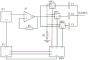
一种宽范围高精度电荷脉冲生成电路,该电荷脉冲生成电路的电荷脉冲输出量范围达四个数量级,包括控制芯片IC2,控制芯片IC2的第一I/O管脚2-1与数模变换芯片IC1的数据输入管脚1-2相连;控制芯片IC2通过I/O管脚2-1控制数模变换芯片IC1的电压输出管脚1-1的电压输出;控制芯片IC2的第二I/O管脚2-2和第三I/O管脚2-3分别与三选一开关SW4的第一控制管脚4-1和第二控制管脚4-2相连;控制芯片IC2的第四I/O管脚2-4与三选一开关SW4的公用管脚4-3相连;控制芯片IC2通过控制第一控制管脚4-1和第二控制管脚4-2的高低电平来控制三选一开关SW4导通的通路,在同一时间三选一开关SW4的公用管脚4-3只会和第一常开管脚4-6、第二常开管脚4-5和第三常开管脚4-4中的其中一个在芯片内部导通;数模变换芯片IC1的电压输出管脚1-1与运算放大器OP的同相输入管脚3-1直接相连;运算放大器OP的反相输入管脚3-2接电阻R1后与运算放大器OP的输出管脚3-3相连;运算放大器OP构成一个电压跟随器提高数模变换芯片IC1的电压驱动能力;运算放大器OP的输出管脚3-3引出后分为三路分别与第一双掷开关SW1的常开管脚5-2、第二双掷开关SW2的常开管脚6-2和第三双掷开关SW3的常开管脚7-2相连;第一双掷开关SW1的常闭管脚5-1、第二双掷开关SW2的常闭管脚6-1和第三双掷开关SW3的常闭管脚7-1彼此相连后通过下拉电阻R2接地,第一双掷开关SW1的公用管脚5-3、第二双掷开关SW2的公用管脚6-3和第三双掷开关SW3的公用管脚7-3分别通过高容值电容器C1、中容值电容器C2和低容值电容器C3后汇聚输出电荷;三选一开关SW4的第一常开管脚4-6、第二常开管脚4-5和第三常开管脚4-4分别与第一双掷开关SW1的控制管脚5-4、第二双掷开关SW2的控制管脚6-4和第三双掷开关SW3的控制管脚7-4相连;三选一开关SW4的三个常开管脚通过高低电平变化控制双掷开关三个双掷开关的通路切换;在同一时间三个双掷开关只有一个开关会发生通路切换。A wide-range high-precision charge pulse generation circuit, the charge pulse output range of the charge pulse generation circuit reaches four orders of magnitude, including a control chip IC2, a first I/O pin 2-1 of the control chip IC2 and a digital-to-analog conversion The data input pins 1-2 of the chip IC1 are connected; the control chip IC2 controls the voltage output of the voltage output pins 1-1 of the digital-to-analog conversion chip IC1 through the I/O pin 2-1; the second I/O pin of the control chip IC2 The O pin 2-2 and the third I/O pin 2-3 are respectively connected with the first control pin 4-1 and the second control pin 4-2 of the three-to-one switch SW4; the fourth control pin of the control chip IC2 The I/O pins 2-4 are connected to the common pin 4-3 of the three-to-one switch SW4; the control chip IC2 controls the high and low levels of the first control pin 4-1 and the second control pin 4-2 to Control the conduction path of the three-to-one switch SW4. At the same time, the common pin 4-3 of the three-to-one switch SW4 will only be connected to the first normally open pin 4-6, the second normally open pin 4-5 and the first normally open pin 4-5. One of the three normally open pins 4-4 is turned on inside the chip; the voltage output pin 1-1 of the digital-to-analog conversion chip IC1 is directly connected to the non-inverting input pin 3-1 of the operational amplifier OP; The inverting input pin 3-2 is connected to the resistor R1 and then connected to the output pin 3-3 of the operational amplifier OP; the operational amplifier OP constitutes a voltage follower to improve the voltage driving capability of the digital-to-analog conversion chip IC1; the output tube of the operational amplifier OP After the pins 3-3 are led out, they are divided into three channels, which are respectively connected with the normally open pin 5-2 of the first double throw switch SW1, the normally open pin 6-2 of the second double throw switch SW2 and the normally open pin 6-2 of the third double throw switch SW3. The open pin 7-2 is connected; the normally closed pin 5-1 of the first double throw switch SW1, the normally closed pin 6-1 of the second double throw switch SW2 and the normally closed pin 7 of the third double throw switch SW3 -1 are connected to each other and grounded through the pull-down resistor R2, the common pin 5-3 of the first double-throw switch SW1, the common pin 6-3 of the second double-throw switch SW2 and the common pin 7 of the third double-throw switch SW3 -3 The output charges are collected through the high-capacitance capacitor C1, the medium-capacity capacitor C2 and the low-capacity capacitor C3 respectively; the first normally open pin 4-6 and the second normally open pin 4- of the three-to-one switch SW4 5 and the third normally open pin 4-4 are respectively connected with the control pin 5-4 of the first double throw switch SW1, the control pin 6-4 of the second double throw switch SW2 and the control pipe of the third double throw switch SW3 Pins 7-4 are connected; the three normally open pins of the three-to-one switch SW4 control the channel switching of the three double-throw switches of the double-throw switch through the change of high and low levels; at the same time, only one switch of the three double-throw switches will have a channel. switch.
所述电阻R1阻值为50欧姆。The resistance value of the resistor R1 is 50 ohms.
所述下拉电阻R2阻值为10k欧姆。The resistance value of the pull-down resistor R2 is 10k ohms.
所述高容值电容器C1容值为10pF。The capacitance value of the high capacitance capacitor C1 is 10pF.
所述中容值电容器C2容值为1pF。The capacitance value of the medium-capacity capacitor C2 is 1pF.
所述低容值电容器C3容值为0.1pF。The capacitance value of the low capacitance capacitor C3 is 0.1pF.
所述的一种宽范围高精度电荷脉冲生成电路的工作方法,上电之后,控制芯片IC2通过第一I/O管脚2-1管脚控制数模变换芯片IC1电压输出管脚1-1的电压输出,数模变换芯片IC1电压输出管脚1-1的电压输入到运算放大器OP组成的电压跟随器提高负载能力并由运算放大器OP的输出管脚3-3输出;控制芯片IC2通过第二I/O管脚2-2和第三I/O管脚2-3控制三选一开关SW4的连通;当控制芯片IC2的第二I/O管脚2-2和第三I/O管脚2-3为低电平时,三选一开关SW4的公用管脚4-3不与三选一开关SW4的任何常开管脚接通;当控制芯片IC2的第二I/O管脚2-2和第三I/O管脚2-3为高电平时,三选一开关SW4的公用管脚4-3与三选一开关SW4的第一常开管脚4-6接通;当控制芯片IC2的第二I/O管脚2-2为高电平,第三I/O管脚2-3为低电平时,三选一开关SW4的公用管脚4-3与三选一开关SW4的第二常开管脚4-5接通;当控制芯片IC2的第二I/O管脚2-2为低电平,第三I/O管脚2-3为高电平时,三选一开关SW4的公用管脚4-3与三选一开关SW4的第四常开管脚4-4接通;The working method of the described wide-range high-precision charge pulse generation circuit, after power-on, the control chip IC2 controls the voltage output pin 1-1 of the digital-to-analog conversion chip IC1 through the first I/O pin 2-1 pin The voltage output of the digital-to-analog conversion chip IC1 voltage output pins 1-1 is input to the voltage follower composed of the operational amplifier OP to improve the load capacity and output by the output pins 3-3 of the operational amplifier OP; the control chip IC2 passes the first The second I/O pin 2-2 and the third I/O pin 2-3 control the connection of the three-to-one switch SW4; when the second I/O pin 2-2 and the third I/O of the control chip IC2 are controlled When the pin 2-3 is low, the common pin 4-3 of the three-to-one switch SW4 is not connected to any normally open pin of the three-to-one switch SW4; when the second I/O pin of the control chip IC2 When 2-2 and the third I/O pin 2-3 are at a high level, the common pin 4-3 of the three-to-one switch SW4 is connected to the first normally open pin 4-6 of the three-to-one switch SW4; When the second I/O pin 2-2 of the control chip IC2 is at a high level and the third I/O pin 2-3 is at a low level, the common pin 4-3 of the three-to-one switch SW4 and the three-to-one switch The second normally open pin 4-5 of a switch SW4 is turned on; when the second I/O pin 2-2 of the control chip IC2 is at a low level and the third I/O pin 2-3 is at a high level , the common pin 4-3 of the three-to-one switch SW4 is connected to the fourth normally open pin 4-4 of the three-to-one switch SW4;
三选一开关SW4的公用管脚4-3与第一常开管脚4-6、第二常开管脚4-5和第三常开管脚4-4中的其中一个接通后,控制芯片IC2的第四I/O管脚2-4输出高电平,切换与三选一开关SW4已经接通的常开管脚相连的双掷开关,三个双掷开关之一闭合后,在与其相连的电容器上充电,形成电荷脉冲输出,电荷脉冲输出量范围达四个数量级。After the common pin 4-3 of the three-to-one switch SW4 is connected to one of the first normally open pin 4-6, the second normally open pin 4-5 and the third normally open pin 4-4, The fourth I/O pins 2-4 of the control chip IC2 output a high level, and switch the double-throw switch connected to the normally open pin of the three-to-one switch SW4 that has been turned on. After one of the three double-throw switches is closed, It is charged on the capacitor connected to it to form a charge pulse output with a range of four orders of magnitude.
本发明电路简单、控制方便、切换迅速,使用三个电容器进行电荷生成,使用三选一开关控制三个电容器的充放电,可以产生几fC到几十pC大范围的精确电荷量电流脉冲。The invention has simple circuit, convenient control and quick switching, uses three capacitors for charge generation, and uses three-to-one switch to control the charge and discharge of the three capacitors, and can generate precise charge current pulses in a wide range from several fC to tens of pC.
附图说明Description of drawings
图1是本发明一种宽范围高精度电荷脉冲生成电路的电路原理图。FIG. 1 is a circuit schematic diagram of a wide-range high-precision charge pulse generating circuit of the present invention.
具体实施方式Detailed ways
为更好地说明本发明,现结合附图对本发明作进一步详细描述。In order to better illustrate the present invention, the present invention will now be described in further detail with reference to the accompanying drawings.
如图1所示,本发明一种宽范围高精度电荷脉冲生成电路,该电荷脉冲生成电路的电荷脉冲输出量范围达四个数量级,包括控制芯片IC2,控制芯片IC2的第一I/O管脚2-1与数模变换芯片IC1的数据输入管脚1-2相连;控制芯片IC2通过I/O管脚2-1控制数模变换芯片IC1的电压输出管脚1-1的电压输出;控制芯片IC2的第二I/O管脚2-2和第三I/O管脚2-3分别与三选一开关SW4的第一控制管脚4-1和第二控制管脚4-2相连;控制芯片IC2的第四I/O管脚2-4与三选一开关SW4的公用管脚4-3相连;控制芯片IC2通过控制第一控制管脚4-1和第二控制管脚4-2的高低电平来控制三选一开关SW4导通的通路,在同一时间三选一开关SW4的公用管脚4-3只会和第一常开管脚4-6、第二常开管脚4-5和第三常开管脚4-4中的其中一个在芯片内部导通;数模变换芯片IC1的电压输出管脚1-1与运算放大器OP的同相输入管脚3-1直接相连;运算放大器OP的反相输入管脚3-2接电阻R1后与运算放大器OP的输出管脚3-3相连;运算放大器OP构成一个电压跟随器提高数模变换芯片IC1的电压驱动能力;运算放大器OP的输出管脚3-3引出后分为三路分别与第一双掷开关SW1的常开管脚5-2、第二双掷开关SW2的常开管脚6-2和第三双掷开关SW3的常开管脚7-2相连;第一双掷开关SW1的常闭管脚5-1、第二双掷开关SW2的常闭管脚6-1和第三双掷开关SW3的常闭管脚7-1彼此相连后通过下拉电阻R2接地,第一双掷开关SW1的公用管脚5-3、第二双掷开关SW2的公用管脚6-3和第三双掷开关SW3的公用管脚7-3分别通过高容值电容器C1、中容值电容器C2和低容值电容器C3后汇聚输出电荷;三选一开关SW4的第一常开管脚4-6、第二常开管脚4-5和第三常开管脚4-4分别与第一双掷开关SW1的控制管脚5-4、第二双掷开关SW2的控制管脚6-4和第三双掷开关SW3的控制管脚7-4相连;三选一开关SW4的三个常开管脚通过高低电平变化控制双掷开关三个双掷开关的通路切换;在同一时间三个双掷开关只有一个开关会发生通路切换。As shown in FIG. 1, the present invention is a wide-range high-precision charge pulse generation circuit, the charge pulse output range of the charge pulse generation circuit reaches four orders of magnitude, including the control chip IC2, the first I/O tube of the control chip IC2 The pin 2-1 is connected to the data input pin 1-2 of the digital-to-analog conversion chip IC1; the control chip IC2 controls the voltage output of the voltage output pin 1-1 of the digital-to-analog conversion chip IC1 through the I/O pin 2-1; The second I/O pin 2-2 and the third I/O pin 2-3 of the control chip IC2 are respectively connected with the first control pin 4-1 and the second control pin 4-2 of the three-to-one switch SW4 Connected; the fourth I/O pin 2-4 of the control chip IC2 is connected with the common pin 4-3 of the three-to-one switch SW4; the control chip IC2 controls the first control pin 4-1 and the second control pin by controlling the The high and low levels of 4-2 control the conduction path of the three-to-one switch SW4. At the same time, the common pin 4-3 of the three-to-one switch SW4 will only be connected to the first normally open pin 4-6 and the second normally open pin 4-6. One of the open pin 4-5 and the third normally open pin 4-4 is turned on inside the chip; the voltage output pin 1-1 of the digital-to-analog conversion chip IC1 and the non-inverting input pin 3- of the operational amplifier OP 1 is directly connected; the inverting input pin 3-2 of the operational amplifier OP is connected to the resistor R1 and then connected to the output pin 3-3 of the operational amplifier OP; the operational amplifier OP constitutes a voltage follower to improve the voltage drive of the digital-to-analog conversion chip IC1 Capability; the output pins 3-3 of the operational amplifier OP are led out and divided into three channels respectively connected to the normally open pins 5-2 of the first double throw switch SW1, the normally open pins 6-2 of the second double throw switch SW2 and The normally open pin 7-2 of the third double throw switch SW3 is connected; the normally closed pin 5-1 of the first double throw switch SW1, the normally closed pin 6-1 of the second double throw switch SW2 and the third double throw switch The normally closed pins 7-1 of the switch SW3 are connected to each other and grounded through the pull-down resistor R2, the common pin 5-3 of the first double throw switch SW1, the common pin 6-3 of the second double throw switch SW2 and the third double throw switch The common pins 7-3 of the throw switch SW3 pass through the high-capacitance capacitor C1, the medium-capacity capacitor C2 and the low-capacity capacitor C3 respectively and then gather the output charges; the first normally open pins 4-6 of the three-to-one switch SW4, The second normally open pin 4-5 and the third normally open pin 4-4 are respectively connected with the control pin 5-4 of the first double throw switch SW1, the control pin 6-4 of the second double throw switch SW2 and the control pin 5-4 of the second double throw switch SW2. The control pins 7-4 of the three-dual-throw switch SW3 are connected; the three normally open pins of the three-to-one switch SW4 control the channel switching of the three double-throw switches of the double-throw switch through the change of high and low levels; at the same time, the three double-throw switches A throw switch has only one switch where the path switching occurs.
作为本发明的优选实施方式,所述电阻R1阻值为50欧姆。As a preferred embodiment of the present invention, the resistance value of the resistor R1 is 50 ohms.
作为本发明的优选实施方式,所述下拉电阻R2阻值为10k欧姆。As a preferred embodiment of the present invention, the resistance value of the pull-down resistor R2 is 10k ohms.
作为本发明的优选实施方式,所述高容值电容器C1容值为10pF。As a preferred embodiment of the present invention, the capacitance value of the high-capacity capacitor C1 is 10pF.
作为本发明的优选实施方式,所述中容值电容器C2容值为1pF。As a preferred embodiment of the present invention, the capacitance value of the medium-capacity capacitor C2 is 1 pF.
作为本发明的优选实施方式,所述低容值电容器C3容值为0.1pF。As a preferred embodiment of the present invention, the capacitance value of the low capacitance capacitor C3 is 0.1pF.
所述的一种宽范围高精度电荷脉冲生成电路的工作方法,上电之后,控制芯片IC2通过第一I/O管脚2-1管脚控制数模变换芯片IC1电压输出管脚1-1的电压输出,数模变换芯片IC1电压输出管脚1-1的电压输入到运算放大器OP组成的电压跟随器提高负载能力并由运算放大器OP的输出管脚3-3输出;控制芯片IC2通过第二I/O管脚2-2和第三I/O管脚2-3控制三选一开关SW4的连通;当控制芯片IC2的第二I/O管脚2-2和第三I/O管脚2-3为低电平时,三选一开关SW4的公用管脚4-3不与三选一开关SW4的任何常开管脚接通;当控制芯片IC2的第二I/O管脚2-2和第三I/O管脚2-3为高电平时,三选一开关SW4的公用管脚4-3与三选一开关SW4的第一常开管脚4-6接通;当控制芯片IC2的第二I/O管脚2-2为高电平,第三I/O管脚2-3为低电平时,三选一开关SW4的公用管脚4-3与三选一开关SW4的第二常开管脚4-5接通;当控制芯片IC2的第二I/O管脚2-2为低电平,第三I/O管脚2-3为高电平时,三选一开关SW4的公用管脚4-3与三选一开关SW4的第四常开管脚4-4接通;The working method of the described wide-range high-precision charge pulse generation circuit, after power-on, the control chip IC2 controls the voltage output pin 1-1 of the digital-to-analog conversion chip IC1 through the first I/O pin 2-1 pin The voltage output of the digital-to-analog conversion chip IC1 voltage output pins 1-1 is input to the voltage follower composed of the operational amplifier OP to improve the load capacity and output by the output pins 3-3 of the operational amplifier OP; the control chip IC2 passes the first The second I/O pin 2-2 and the third I/O pin 2-3 control the connection of the three-to-one switch SW4; when the second I/O pin 2-2 and the third I/O of the control chip IC2 are controlled When the pin 2-3 is low, the common pin 4-3 of the three-to-one switch SW4 is not connected to any normally open pin of the three-to-one switch SW4; when the second I/O pin of the control chip IC2 When 2-2 and the third I/O pin 2-3 are at a high level, the common pin 4-3 of the three-to-one switch SW4 is connected to the first normally open pin 4-6 of the three-to-one switch SW4; When the second I/O pin 2-2 of the control chip IC2 is at a high level and the third I/O pin 2-3 is at a low level, the common pin 4-3 of the three-to-one switch SW4 and the three-to-one switch The second normally open pin 4-5 of a switch SW4 is turned on; when the second I/O pin 2-2 of the control chip IC2 is at a low level and the third I/O pin 2-3 is at a high level , the common pin 4-3 of the three-to-one switch SW4 is connected to the fourth normally open pin 4-4 of the three-to-one switch SW4;
三选一开关SW4的公用管脚4-3与第一常开管脚4-6、第二常开管脚4-5和第三常开管脚4-4中的其中一个接通后,控制芯片IC2的第四I/O管脚2-4输出高电平,切换与三选一开关SW4已经接通的常开管脚相连的双掷开关,三个双掷开关之一闭合后,在与其相连的电容器上充电,形成电荷脉冲输出,电荷脉冲输出量范围达四个数量级。After the common pin 4-3 of the three-to-one switch SW4 is connected to one of the first normally open pin 4-6, the second normally open pin 4-5 and the third normally open pin 4-4, The fourth I/O pins 2-4 of the control chip IC2 output a high level, and switch the double-throw switch connected to the normally open pin of the three-to-one switch SW4 that has been turned on. After one of the three double-throw switches is closed, It is charged on the capacitor connected to it to form a charge pulse output with a range of four orders of magnitude.
Claims (7)
Priority Applications (1)
| Application Number | Priority Date | Filing Date | Title |
|---|---|---|---|
| CN202010576666.7A CN111786659A (en) | 2020-06-22 | 2020-06-22 | A wide-range high-precision charge pulse generating circuit and working method |
Applications Claiming Priority (1)
| Application Number | Priority Date | Filing Date | Title |
|---|---|---|---|
| CN202010576666.7A CN111786659A (en) | 2020-06-22 | 2020-06-22 | A wide-range high-precision charge pulse generating circuit and working method |
Publications (1)
| Publication Number | Publication Date |
|---|---|
| CN111786659A true CN111786659A (en) | 2020-10-16 |
Family
ID=72757011
Family Applications (1)
| Application Number | Title | Priority Date | Filing Date |
|---|---|---|---|
| CN202010576666.7A Pending CN111786659A (en) | 2020-06-22 | 2020-06-22 | A wide-range high-precision charge pulse generating circuit and working method |
Country Status (1)
| Country | Link |
|---|---|
| CN (1) | CN111786659A (en) |
Citations (7)
| Publication number | Priority date | Publication date | Assignee | Title |
|---|---|---|---|---|
| GB1180259A (en) * | 1966-12-13 | 1970-02-04 | Commissariat Energie Atomique | Apparatus for the Collection and Logarithmic Measurement of Quantities of Charges Produced by an Ionization Chamber |
| US20030164888A1 (en) * | 1994-06-01 | 2003-09-04 | Simage, Oy | Imaging devices, systems and methods |
| CN1732377A (en) * | 2002-12-25 | 2006-02-08 | 浜松光子学株式会社 | Optical sensor |
| US20110156764A1 (en) * | 2009-12-30 | 2011-06-30 | Industrial Technology Research Institute | Method for calibrating and controlling signal slew rate, and output stage using the same |
| CN102246510A (en) * | 2008-12-12 | 2011-11-16 | E2V半导体公司 | Image sensor utilizing dual charge transfer for large dynamic range and readout method |
| CN104316950A (en) * | 2014-10-17 | 2015-01-28 | 吴雪梅 | Method and device for low-power radiation dose rate detection and wide-range scaling graduation |
| EP2974032A1 (en) * | 2013-03-11 | 2016-01-20 | Microchip Technology Incorporated | 4n+1 level capacitive dac using n capacitors |
-
2020
- 2020-06-22 CN CN202010576666.7A patent/CN111786659A/en active Pending
Patent Citations (7)
| Publication number | Priority date | Publication date | Assignee | Title |
|---|---|---|---|---|
| GB1180259A (en) * | 1966-12-13 | 1970-02-04 | Commissariat Energie Atomique | Apparatus for the Collection and Logarithmic Measurement of Quantities of Charges Produced by an Ionization Chamber |
| US20030164888A1 (en) * | 1994-06-01 | 2003-09-04 | Simage, Oy | Imaging devices, systems and methods |
| CN1732377A (en) * | 2002-12-25 | 2006-02-08 | 浜松光子学株式会社 | Optical sensor |
| CN102246510A (en) * | 2008-12-12 | 2011-11-16 | E2V半导体公司 | Image sensor utilizing dual charge transfer for large dynamic range and readout method |
| US20110156764A1 (en) * | 2009-12-30 | 2011-06-30 | Industrial Technology Research Institute | Method for calibrating and controlling signal slew rate, and output stage using the same |
| EP2974032A1 (en) * | 2013-03-11 | 2016-01-20 | Microchip Technology Incorporated | 4n+1 level capacitive dac using n capacitors |
| CN104316950A (en) * | 2014-10-17 | 2015-01-28 | 吴雪梅 | Method and device for low-power radiation dose rate detection and wide-range scaling graduation |
Non-Patent Citations (5)
| Title |
|---|
| 《中国集成电路大全》编委会: "《中国集成电路大全 高速CMOS集成电路》", 31 August 1995, 国防工业出版社 * |
| A. CASTOLDI: "Qualification of a high-resolution on-chip injection circuit for the calibration of the DSSC X-ray imager for the European XFEL", 《2018 IEEE NUCLEAR SCIENCE SYMPOSIUM AND MEDICAL IMAGING CONFERENCE PROCEEDINGS (NSS/MIC)》 * |
| 刘真: "《数字逻辑与计算机设计基础》", 30 June 2003, 高等教育出版社 * |
| 杨海波: "DAMPE-PSD读出电子学研制", 《原子能科学技术》 * |
| 阿蒂克斯: "《放射物理和辐射剂量学导论》", 31 May 2013, 中国原子能出版社 * |
Similar Documents
| Publication | Publication Date | Title |
|---|---|---|
| CN103383404B (en) | Current measurement circuit | |
| CN204613137U (en) | Air-anion concentration detector | |
| US3959653A (en) | Fast charge digitizer and digital data acquisition system for measuring time varying radiation fields | |
| CN106841749B (en) | It is a kind of to realize two-way high-side current detection circuit using single amplifier | |
| CN112165329B (en) | A Capacitance-to-Digital Converter Based on SAR Logic to Eliminate Parasitics | |
| CN102957430A (en) | Modulus switching circuit | |
| CN112213554A (en) | A weak current measurement circuit and method based on current frequency conversion method | |
| CN105842539B (en) | Resistance measuring system based on FPGA-TDC and method | |
| CN114964318B (en) | An asynchronous capacitance sensor interface circuit with self-calibration function | |
| CN111786659A (en) | A wide-range high-precision charge pulse generating circuit and working method | |
| CN216351253U (en) | X, gamma radiation detection circuit based on ionization chamber detector | |
| CN101533099A (en) | Charge frequency converter | |
| JP2896371B2 (en) | Pressure sensor | |
| CN210294391U (en) | Current measurement circuit based on I-F conversion | |
| CN103888128A (en) | Array capacitive sensor interface circuit based on interleaving timing sequence detection cancellation mechanism | |
| CN119509719A (en) | Photon number resolvable detection system and method | |
| CN112881775A (en) | Low-power-consumption high-resolution capacitance measuring circuit | |
| CN114720755B (en) | A front-end readout electronics circuit for a particle detector | |
| CN106569008A (en) | Novel broadband peak detection circuit | |
| CN115560662A (en) | A PVDF piezoelectric sensor strain measurement circuit conditioning device | |
| Jagdish et al. | A preamplifier-shaper-stretcher integrated circuit system for use with germanium strip detectors | |
| CN110133708B (en) | A kind of measuring device and measuring method of nuclear pulse signal | |
| CN209844937U (en) | Digital differential charge-to-digital converter | |
| CN219833791U (en) | Power supply control device and charging and discharging system | |
| CN110244133A (en) | A kind of single pulse width measuring circuit and measurement method |
Legal Events
| Date | Code | Title | Description |
|---|---|---|---|
| PB01 | Publication | ||
| PB01 | Publication | ||
| SE01 | Entry into force of request for substantive examination | ||
| SE01 | Entry into force of request for substantive examination | ||
| RJ01 | Rejection of invention patent application after publication |
Application publication date: 20201016 |
|
| RJ01 | Rejection of invention patent application after publication |