CN111697959B - Electric heating equipment and its touch device - Google Patents
Electric heating equipment and its touch device Download PDFInfo
- Publication number
- CN111697959B CN111697959B CN201910196735.9A CN201910196735A CN111697959B CN 111697959 B CN111697959 B CN 111697959B CN 201910196735 A CN201910196735 A CN 201910196735A CN 111697959 B CN111697959 B CN 111697959B
- Authority
- CN
- China
- Prior art keywords
- light
- sensing
- opening
- touch device
- substrate
- Prior art date
- Legal status (The legal status is an assumption and is not a legal conclusion. Google has not performed a legal analysis and makes no representation as to the accuracy of the status listed.)
- Active
Links
Images


Classifications
-
- H—ELECTRICITY
- H05—ELECTRIC TECHNIQUES NOT OTHERWISE PROVIDED FOR
- H05K—PRINTED CIRCUITS; CASINGS OR CONSTRUCTIONAL DETAILS OF ELECTRIC APPARATUS; MANUFACTURE OF ASSEMBLAGES OF ELECTRICAL COMPONENTS
- H05K5/00—Casings, cabinets or drawers for electric apparatus
- H05K5/0017—Casings, cabinets or drawers for electric apparatus with operator interface units
-
- H—ELECTRICITY
- H05—ELECTRIC TECHNIQUES NOT OTHERWISE PROVIDED FOR
- H05K—PRINTED CIRCUITS; CASINGS OR CONSTRUCTIONAL DETAILS OF ELECTRIC APPARATUS; MANUFACTURE OF ASSEMBLAGES OF ELECTRICAL COMPONENTS
- H05K3/00—Apparatus or processes for manufacturing printed circuits
- H05K3/36—Assembling printed circuits with other printed circuits
- H05K3/368—Assembling printed circuits with other printed circuits parallel to each other
-
- H—ELECTRICITY
- H03—ELECTRONIC CIRCUITRY
- H03K—PULSE TECHNIQUE
- H03K17/00—Electronic switching or gating, i.e. not by contact-making and –breaking
- H03K17/94—Electronic switching or gating, i.e. not by contact-making and –breaking characterised by the way in which the control signals are generated
- H03K17/96—Touch switches
- H03K17/9627—Optical touch switches
-
- F—MECHANICAL ENGINEERING; LIGHTING; HEATING; WEAPONS; BLASTING
- F24—HEATING; RANGES; VENTILATING
- F24C—DOMESTIC STOVES OR RANGES ; DETAILS OF DOMESTIC STOVES OR RANGES, OF GENERAL APPLICATION
- F24C7/00—Stoves or ranges heated by electric energy
- F24C7/08—Arrangement or mounting of control or safety devices
- F24C7/082—Arrangement or mounting of control or safety devices on ranges, e.g. control panels, illumination
- F24C7/083—Arrangement or mounting of control or safety devices on ranges, e.g. control panels, illumination on tops, hot plates
-
- F—MECHANICAL ENGINEERING; LIGHTING; HEATING; WEAPONS; BLASTING
- F24—HEATING; RANGES; VENTILATING
- F24C—DOMESTIC STOVES OR RANGES ; DETAILS OF DOMESTIC STOVES OR RANGES, OF GENERAL APPLICATION
- F24C7/00—Stoves or ranges heated by electric energy
- F24C7/08—Arrangement or mounting of control or safety devices
- F24C7/082—Arrangement or mounting of control or safety devices on ranges, e.g. control panels, illumination
- F24C7/086—Arrangement or mounting of control or safety devices on ranges, e.g. control panels, illumination touch control
-
- H—ELECTRICITY
- H05—ELECTRIC TECHNIQUES NOT OTHERWISE PROVIDED FOR
- H05B—ELECTRIC HEATING; ELECTRIC LIGHT SOURCES NOT OTHERWISE PROVIDED FOR; CIRCUIT ARRANGEMENTS FOR ELECTRIC LIGHT SOURCES, IN GENERAL
- H05B1/00—Details of electric heating devices
- H05B1/02—Automatic switching arrangements specially adapted to apparatus ; Control of heating devices
- H05B1/0202—Switches
-
- H—ELECTRICITY
- H05—ELECTRIC TECHNIQUES NOT OTHERWISE PROVIDED FOR
- H05B—ELECTRIC HEATING; ELECTRIC LIGHT SOURCES NOT OTHERWISE PROVIDED FOR; CIRCUIT ARRANGEMENTS FOR ELECTRIC LIGHT SOURCES, IN GENERAL
- H05B3/00—Ohmic-resistance heating
- H05B3/20—Heating elements having extended surface area substantially in a two-dimensional [2D] plane, e.g. plate-heater
-
- H—ELECTRICITY
- H05—ELECTRIC TECHNIQUES NOT OTHERWISE PROVIDED FOR
- H05K—PRINTED CIRCUITS; CASINGS OR CONSTRUCTIONAL DETAILS OF ELECTRIC APPARATUS; MANUFACTURE OF ASSEMBLAGES OF ELECTRICAL COMPONENTS
- H05K1/00—Printed circuits
- H05K1/02—Details
- H05K1/0274—Optical details, e.g. printed circuits comprising integral optical means
-
- H—ELECTRICITY
- H01—ELECTRIC ELEMENTS
- H01R—ELECTRICALLY-CONDUCTIVE CONNECTIONS; STRUCTURAL ASSOCIATIONS OF A PLURALITY OF MUTUALLY-INSULATED ELECTRICAL CONNECTING ELEMENTS; COUPLING DEVICES; CURRENT COLLECTORS
- H01R12/00—Structural associations of a plurality of mutually-insulated electrical connecting elements, specially adapted for printed circuits, e.g. printed circuit boards [PCB], flat or ribbon cables, or like generally planar structures, e.g. terminal strips, terminal blocks; Coupling devices specially adapted for printed circuits, flat or ribbon cables, or like generally planar structures; Terminals specially adapted for contact with, or insertion into, printed circuits, flat or ribbon cables, or like generally planar structures
- H01R12/70—Coupling devices
- H01R12/71—Coupling devices for rigid printing circuits or like structures
-
- H—ELECTRICITY
- H05—ELECTRIC TECHNIQUES NOT OTHERWISE PROVIDED FOR
- H05K—PRINTED CIRCUITS; CASINGS OR CONSTRUCTIONAL DETAILS OF ELECTRIC APPARATUS; MANUFACTURE OF ASSEMBLAGES OF ELECTRICAL COMPONENTS
- H05K1/00—Printed circuits
- H05K1/18—Printed circuits structurally associated with non-printed electric components
-
- H—ELECTRICITY
- H05—ELECTRIC TECHNIQUES NOT OTHERWISE PROVIDED FOR
- H05K—PRINTED CIRCUITS; CASINGS OR CONSTRUCTIONAL DETAILS OF ELECTRIC APPARATUS; MANUFACTURE OF ASSEMBLAGES OF ELECTRICAL COMPONENTS
- H05K2201/00—Indexing scheme relating to printed circuits covered by H05K1/00
- H05K2201/04—Assemblies of printed circuits
- H05K2201/042—Stacked spaced PCBs; Planar parts of folded flexible circuits having mounted components in between or spaced from each other
-
- H—ELECTRICITY
- H05—ELECTRIC TECHNIQUES NOT OTHERWISE PROVIDED FOR
- H05K—PRINTED CIRCUITS; CASINGS OR CONSTRUCTIONAL DETAILS OF ELECTRIC APPARATUS; MANUFACTURE OF ASSEMBLAGES OF ELECTRICAL COMPONENTS
- H05K2201/00—Indexing scheme relating to printed circuits covered by H05K1/00
- H05K2201/09—Shape and layout
- H05K2201/09009—Substrate related
- H05K2201/09063—Holes or slots in insulating substrate not used for electrical connections
-
- H—ELECTRICITY
- H05—ELECTRIC TECHNIQUES NOT OTHERWISE PROVIDED FOR
- H05K—PRINTED CIRCUITS; CASINGS OR CONSTRUCTIONAL DETAILS OF ELECTRIC APPARATUS; MANUFACTURE OF ASSEMBLAGES OF ELECTRICAL COMPONENTS
- H05K2201/00—Indexing scheme relating to printed circuits covered by H05K1/00
- H05K2201/10—Details of components or other objects attached to or integrated in a printed circuit board
- H05K2201/10007—Types of components
- H05K2201/10106—Light emitting diode [LED]
-
- H—ELECTRICITY
- H05—ELECTRIC TECHNIQUES NOT OTHERWISE PROVIDED FOR
- H05K—PRINTED CIRCUITS; CASINGS OR CONSTRUCTIONAL DETAILS OF ELECTRIC APPARATUS; MANUFACTURE OF ASSEMBLAGES OF ELECTRICAL COMPONENTS
- H05K2201/00—Indexing scheme relating to printed circuits covered by H05K1/00
- H05K2201/10—Details of components or other objects attached to or integrated in a printed circuit board
- H05K2201/10007—Types of components
- H05K2201/10151—Sensor
-
- H—ELECTRICITY
- H05—ELECTRIC TECHNIQUES NOT OTHERWISE PROVIDED FOR
- H05K—PRINTED CIRCUITS; CASINGS OR CONSTRUCTIONAL DETAILS OF ELECTRIC APPARATUS; MANUFACTURE OF ASSEMBLAGES OF ELECTRICAL COMPONENTS
- H05K2201/00—Indexing scheme relating to printed circuits covered by H05K1/00
- H05K2201/10—Details of components or other objects attached to or integrated in a printed circuit board
- H05K2201/10007—Types of components
- H05K2201/10189—Non-printed connector
-
- H—ELECTRICITY
- H05—ELECTRIC TECHNIQUES NOT OTHERWISE PROVIDED FOR
- H05K—PRINTED CIRCUITS; CASINGS OR CONSTRUCTIONAL DETAILS OF ELECTRIC APPARATUS; MANUFACTURE OF ASSEMBLAGES OF ELECTRICAL COMPONENTS
- H05K2201/00—Indexing scheme relating to printed circuits covered by H05K1/00
- H05K2201/20—Details of printed circuits not provided for in H05K2201/01 - H05K2201/10
- H05K2201/2018—Presence of a frame in a printed circuit or printed circuit assembly
Landscapes
- Engineering & Computer Science (AREA)
- Microelectronics & Electronic Packaging (AREA)
- Chemical & Material Sciences (AREA)
- Combustion & Propulsion (AREA)
- Mechanical Engineering (AREA)
- General Engineering & Computer Science (AREA)
- Manufacturing & Machinery (AREA)
- Switches That Are Operated By Magnetic Or Electric Fields (AREA)
Abstract
本发明公开了一种电热设备及其触控装置。前述触控装置包括:基板、发光元件、遮光件、感应板以及透光板。发光元件设置于前述基板上。遮光件设置于前述基板上,其中前述遮光件具有一第一开口,且前述发光元件位于前述第一开口中。感应板设置于前述遮光件上,并电性连接至前述基板,其中前述感应板具有一第二开口,且前述第一开口与前述第二开口重叠。透光板设置于前述感应板上,且覆盖前述第一开口及前述第二开口。

The invention discloses an electric heating device and a touch control device thereof. The aforementioned touch device includes: a substrate, a light-emitting element, a light-shielding element, a sensing plate, and a light-transmitting plate. The light emitting element is arranged on the aforementioned substrate. The light-shielding element is disposed on the aforementioned substrate, wherein the aforementioned light-shielding element has a first opening, and the aforementioned light-emitting element is located in the aforementioned first opening. The sensing plate is disposed on the light shielding element and is electrically connected to the substrate, wherein the sensing plate has a second opening, and the first opening overlaps with the second opening. The transparent plate is disposed on the sensing plate and covers the first opening and the second opening.
Description
技术领域technical field
本发明是有关于一种电热设备及其触控装置,特别是有关于一种包括设置有开口的感应板的触控装置。The present invention relates to an electric heating device and a touch device thereof, in particular to a touch device including a sensing plate provided with an opening.
背景技术Background technique
随着科技的发展,触控技术已应用于各种电子产品上,以提供用户更佳的操作体验。现有触控装置的传感器通常于透光软板内埋入导电线路,再于前述软板上印刷隔光油墨或漆,留下未印刷的部分为需透光的图案。由于软板需使用具有特定透光率的特殊材料,且需要进行印刷工艺,使得工艺成本较高,并难以缩小整体的尺寸。此外,为了显示触控装置的图案,需将发光二极管(light-emitting diode;LED)或其他类似的照明装置安装于传感器下方。然而,照明装置所照亮的区域往往会与原本设计的范围有落差。With the development of technology, touch technology has been applied to various electronic products to provide users with better operating experience. The sensors of existing touch devices usually embed conductive circuits in the light-transmitting flexible board, and then print light-shielding ink or varnish on the aforementioned flexible board, leaving the unprinted part as the pattern that needs to be light-transmitting. Since the flexible board needs to use a special material with a specific light transmittance, and requires a printing process, the process cost is relatively high, and it is difficult to reduce the overall size. In addition, in order to display the pattern of the touch device, light-emitting diodes (light-emitting diodes; LEDs) or other similar lighting devices need to be installed under the sensor. However, the area illuminated by the lighting device often falls short of the originally designed range.
发明内容Contents of the invention
为了解决上述问题,本发明的一些实施例提供一种触控装置,包括:基板、发光元件、遮光件、感应板以及透光板。发光元件设置于前述基板上。遮光件设置于前述基板上,其中前述遮光件具有一第一开口,且前述发光元件位于前述第一开口中。感应板设置于前述遮光件上,并电性连接至前述基板,其中前述感应板具有一第二开口,且前述第一开口与前述第二开口重叠。透光板设置于前述感应板上,且覆盖前述第一开口及前述第二开口。In order to solve the above problems, some embodiments of the present invention provide a touch device, including: a substrate, a light-emitting element, a light-shielding element, a sensing plate, and a light-transmitting plate. The light emitting element is arranged on the aforementioned substrate. The light-shielding element is disposed on the aforementioned substrate, wherein the aforementioned light-shielding element has a first opening, and the aforementioned light-emitting element is located in the aforementioned first opening. The sensing plate is disposed on the light shielding element and electrically connected to the substrate, wherein the sensing plate has a second opening, and the first opening overlaps with the second opening. The transparent plate is disposed on the sensing plate and covers the first opening and the second opening.
在一些实施例中,前述触控装置更包括薄膜,设置于前述感应板与前述透光板之间。图样形成在前述薄膜上,且前述发光元件所发出的光可穿透前述薄膜,并显示前述图样。在一些实施例中,图样形成在前述透光板上,且前述发光元件所发出的光可穿透前述透光板,并显示前述图样。In some embodiments, the aforementioned touch device further includes a thin film disposed between the aforementioned sensing plate and the aforementioned light-transmitting plate. The pattern is formed on the aforementioned thin film, and the light emitted by the aforementioned light-emitting element can penetrate the aforementioned thin film and display the aforementioned pattern. In some embodiments, the pattern is formed on the light-transmitting plate, and the light emitted by the light-emitting element can pass through the light-transmitting plate to display the pattern.
在一些实施例中,前述感应板更包括感应电路,围绕前述第二开口,其中前述感应电路包括多个接点,且前述接点以并联的方式设置。在一些实施例中,前述基板更包括第一连接件,前述感应板更包括第二连接件,且前述第一连接件与前述第二连接件电性连接。前述遮光件更具有孔洞,且前述第一连接件与前述第二连接件透过前述孔洞电性连接。In some embodiments, the sensing plate further includes a sensing circuit surrounding the second opening, wherein the sensing circuit includes a plurality of contacts, and the contacts are arranged in parallel. In some embodiments, the aforementioned substrate further includes a first connecting element, the aforementioned induction board further includes a second connecting element, and the aforementioned first connecting element is electrically connected to the aforementioned second connecting element. The aforementioned light-shielding element further has a hole, and the aforementioned first connecting element and the aforementioned second connecting element are electrically connected through the aforementioned hole.
在一些实施例中,前述感应板更包括第一感应板及第二感应板,前述第一感应板位于前述第二感应板的开孔内部,且与前述第二感应板电性隔离。In some embodiments, the sensing board further includes a first sensing board and a second sensing board, and the first sensing board is located inside the opening of the second sensing board and is electrically isolated from the second sensing board.
本发明的一些实施例提供一种电热设备,包括:本体、加热装置以及触控装置,其中前述加热装置设置于前述本体中。触控装置设置于前述本体中,并控制加热装置的操作状态。触控装置包括:基板、多个发光元件、遮光件、感应板以及透光板。发光元件设置于前述基板上。遮光件设置于前述基板上,其中前述遮光件具有多个第一开口,且前述发光元件对应位于前述第一开口中。感应板设置于前述遮光件上,并电性连接至前述基板,其中前述感应板具有多个第二开口,且前述第一开口与前述第二开口对应重叠。透光板设置于前述感应板上,且覆盖前述第一开口及前述第二开口。Some embodiments of the present invention provide an electric heating device, including: a body, a heating device, and a touch device, wherein the heating device is disposed in the body. The touch device is arranged in the body and controls the operation state of the heating device. The touch device includes: a substrate, a plurality of light-emitting elements, a light-shielding element, a sensing plate and a light-transmitting plate. The light emitting element is arranged on the aforementioned substrate. The light-shielding element is disposed on the aforementioned substrate, wherein the aforementioned light-shielding element has a plurality of first openings, and the aforementioned light-emitting elements are correspondingly located in the aforementioned first openings. The sensing plate is disposed on the light-shielding element and is electrically connected to the substrate, wherein the sensing plate has a plurality of second openings, and the first openings and the second openings overlap correspondingly. The transparent plate is disposed on the sensing plate and covers the first opening and the second opening.
为让本发明的上述和其他目的、特征和优点能更明显易懂,下文特举出较佳实施例,并配合所附图式,做详细说明如下。In order to make the above and other objects, features and advantages of the present invention more comprehensible, preferred embodiments are listed below and described in detail in conjunction with the accompanying drawings.
附图说明Description of drawings
图1显示根据本发明一实施例的触控装置的立体示意图。FIG. 1 shows a schematic perspective view of a touch device according to an embodiment of the invention.
图2显示图1的触控装置的爆炸示意图。FIG. 2 shows an exploded view of the touch device in FIG. 1 .
图3显示图1的触控装置沿线A-A’的剖视示意图。FIG. 3 shows a schematic cross-sectional view of the touch device of FIG. 1 along the line A-A'.
图4显示根据本发明另一实施例的触控装置的爆炸示意图。FIG. 4 shows an exploded view of a touch device according to another embodiment of the present invention.
图5A至5D显示根据本发明一些实施例的感应板的上视示意图。5A to 5D show schematic top views of sensing pads according to some embodiments of the present invention.
图6显示根据本发明一实施例的电热设备的上视示意图。Fig. 6 shows a schematic top view of an electrothermal device according to an embodiment of the present invention.
图7显示根据图6所示的触控装置的爆炸示意图。FIG. 7 shows an exploded view of the touch device shown in FIG. 6 .
图8显示根据本发明另一实施例的触控装置的爆炸示意图。FIG. 8 shows an exploded view of a touch device according to another embodiment of the present invention.
其中,附图标记位:Among them, the reference sign bit:
1~电热设备;1~Electric heating equipment;
10、10A、10’、10”~触控装置;10, 10A, 10’, 10”~touch device;
11、11’~基板;11, 11'~substrate;
111、111A、111B~第一连接件;111, 111A, 111B~the first connecting piece;
12、12’~发光元件;12, 12'~light-emitting element;
13、13’、13”~遮光件;13, 13’, 13”~shading piece;
131、131’~第一开口;131, 131'~the first opening;
132、132’、132A、132B~孔洞;132, 132', 132A, 132B ~ holes;
14、14A、14B、14C、14D、14’~感应板;14, 14A, 14B, 14C, 14D, 14'~sensing plate;
14A’~第一感应板;14A'~the first induction plate;
14B’~第二感应板;14B'~the second induction plate;
141、141’~第二开口;141, 141'~the second opening;
141B~开孔;141B~opening hole;
142、142A、142B、142C、142D、142’、1422~感应电路;142, 142A, 142B, 142C, 142D, 142', 1422~sensing circuit;
143~第二连接件;143~the second connector;
144A、144B、144C、144D~接点;144A, 144B, 144C, 144D~contact;
15~透光板;15 ~ light-transmitting board;
16、16’~薄膜;16, 16'~film;
17、17’~图样;17, 17'~pattern;
20~本体;20 ~ body;
30~加热装置;30 ~ heating device;
A-A’~线;A-A'~line;
L~光L ~ light
具体实施方式Detailed ways
以下说明本发明实施例的触控装置。然而,可轻易了解本发明实施例提供许多合适的发明概念而可实施于广泛的各种特定背景。所揭示的特定实施例仅仅用于说明以特定方法使用本发明,并非用以局限本发明的范围。The touch device of the embodiment of the present invention is described below. It should be readily appreciated, however, that the embodiments of the invention provide many suitable inventive concepts that can be implemented in a wide variety of specific contexts. The specific embodiments disclosed are merely illustrative of specific ways to use the invention and do not limit the scope of the invention.
除非另外定义,在此使用的全部用语(包括技术及科学用语)具有与此篇揭露所属的一般技艺者所通常理解的相同涵义。能理解的是这些用语,例如在通常使用的字典中定义的用语,应被解读成具有一与相关技术及本揭露的背景或上下文一致的意思,而不应以一理想化或过度正式的方式解读,除非在此特别定义。Unless otherwise defined, all terms (including technical and scientific terms) used herein have the same meaning as commonly understood by one of ordinary skill in the art to which this disclosure belongs. It is understood that these terms, such as those defined in commonly used dictionaries, should be interpreted as having a meaning consistent with the background or context of the related art and the present disclosure, and not in an idealized or overly formal manner Interpretation, unless specifically defined herein.
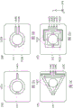
请先参照图1,图1显示根据本发明一实施例的触控装置10的立体示意图。应先说明的是,在本实施例中的触控装置10可设置于各种电子设备中,并可感测外界所施加的力,产生电信号传递至电子设备内的控制单元(未图标)。前述控制单元可根据前述电信号,切换电子设备的操作状态及/或显示不同的图样,藉以达到触控的功能。Please refer to FIG. 1 first. FIG. 1 shows a perspective view of a
请参照图2,图2显示图1的触控装置10的爆炸示意图。在本实施例中,触控装置10包括基板11、发光元件12、遮光件13、感应板14、透光板15及薄膜16。举例而言,基板11可以是一印刷电路板(printed circuit board;PCB)或任何其他设置有电路的基板。在基板11上设置有第一连接件111,以与触控装置10的感应板14电性连接。发光元件12设置于基板11上,其中发光元件12可以是发光二极管(LED)或任何其他可用以发光的元件。遮光件13设置于基板11上,并具有贯穿遮光件13的第一开口131,其中发光元件12设置于第一开口131中,使得发光元件12所发出的光L(图3)可通过遮光件13而传递至外界。Please refer to FIG. 2 . FIG. 2 shows an exploded view of the
感应板14设置于遮光件13上,其中感应板14具有第二开口141,对应于遮光件13的第一开口131。举例而言,如图3所示,由一垂直方向(Z轴)观察,第二开口141会与第一开口131大致上重叠。此外,感应板14更包括感应电路142,设置于第二开口141周围,用以感测外界(例如使用者)对感应板14所施加的力。当感应电路142感测到手指接近时,感应式电容的容值会产生变化,感应电路142会产生电信号。感应板14更设置有第二连接件143,透过遮光件13的孔洞132与第一连接件111电性连接,藉以使感应电路142与基板11中的电路(未图标)电性连接,进而将电信号传递至设置于电子设备内的控制单元,使得电子设备可根据前述电信号来进行各种不同的操作。The
举例而言,第一连接件111与第二连接件143可以是连接器、固定式导体(例如:金属桥)或弹性接触元件(例如:金属弹簧、导电橡胶、电缆线(cable)、软扁平电缆(flexibleflat cable;FFC)及可挠性印刷电路板(flexible printed circuit board;FPC)等)。在本实施例中,遮光件13的第一开口131设置于遮光件13的中央,而孔洞132则设置于第一开口131旁。然而,亦可根据需求将第一开口131及孔洞132配置于遮光件13中任何其他适合的位置。For example, the first connecting
此外,薄膜16设置于感应板14上,其中薄膜16例如由透明、导光的材质制成,使发光元件12所发出的光可穿过薄膜16。在本实施例中,薄膜16上形成有图样17,其中图样17可透过印刷、喷涂或任何其他适合的方式形成于薄膜16上,使得光线穿过薄膜16之后,显示出图样17的全部或部分图样。另外,透光板15设置于薄膜16上。举例而言,透光板15可以是陶瓷玻璃(ceramic glass)或任何其他具有特定硬度的透明材料,藉以同时达到保护触控装置10以及使光得以穿透的效果。In addition, the
请参照图4,图4显示根据本发明另一实施例的触控装置10A的爆炸示意图。在本实施例中,可省略薄膜16,而直接将图样17以印刷或烧结的方式形成于透光板15上,藉以降低触控装置10的整体厚度。无论是将图样17形成于薄膜16或透光板15上,在图样17非形成于感应板14上的情况下,可简化感应板14的工艺。另外,感应板14可使用非透明的材料,进而可根据需求使用其他成本较低或强度更高的材料。Please refer to FIG. 4 , which shows an exploded view of a
图5A至5D显示根据本发明一些实施例的感应板的上视示意图。如图5A所示,感应板14A的感应电路142A设置于第二开口141周围,其中感应电路142A具有一个接点144A,藉以将感应电路142A因感测手指接近时,感应式电容的容值会产生变化,所产生的电信号传递至基板11的电路(未图标)。在其他一些实施例中,感应电路可具有多个接点。如图5B所示,感应电路142B设置于第二开口141周围,并分为两个部分。感应电路142B的两个部分皆具有接点144B。应了解的是,上述接点144B是以并联的方式与基板11的电路电性连接。如此一来,即使接点144B的其中之一失效,仍可经由另外一个未失效的接点传递电信号,使得触控装置可维持正常运作,藉此可降低触控装置的故障率。5A to 5D show schematic top views of sensing pads according to some embodiments of the present invention. As shown in FIG. 5A, the
此外,亦可根据设计需求,将感应电路设计成不同的形状。如图5C所示,感应电路142C设置成位于第二开口141周围的三角形,且分为三个部分,感应电路142C的三个部分皆具有接点144C。再者,如图5D所示,感应电路142D设置成位于第二开口141周围的矩形,且分为四个部分,感应电路142D的四个部分皆具有接点144D。可理解的是,将感应电路分为愈多个部分(亦即感应电路具有愈多个接点),则触控装置故障的机率就愈低。此外,应注意的是,虽然以上实施例列举出感应电路的形状与其接点数量的各种范例,然而本发明所属技术领域中具有通常知识者可根据需求而将感应电路的形状与接点数量进行任意的搭配。In addition, the sensing circuit can also be designed into different shapes according to design requirements. As shown in FIG. 5C , the
图6显示根据本发明一实施例的电热设备1的上视示意图。电热设备1包括触控装置10’、本体20及加热装置30,加热装置30设置于本体20中。举例而言,加热装置30可以为一电阻,并藉由施加电流来产生热能。然而,加热装置30可以为任何其他可产生热能的装置。触控装置10’设置于本体20中,有关于触控装置10’的详细结构,以下将配合图6进行更进一步的说明。触控装置10’用以控制加热装置30的操作状态(例如是否运作以产生热能),或者控制加热装置30产生热能的强度等参数。此外,触控装置10’亦可根据加热装置30的状态而显示不同的信息。应理解的是,虽然在本实施例中将触控装置10’用于电热设备1中,但触控装置10’亦可设置于其他电子装置中,并可用来控制前述电子装置的操作状态。Fig. 6 shows a schematic top view of the electric heating device 1 according to an embodiment of the present invention. The electric heating device 1 includes a
图7显示图6的触控装置10’的爆炸示意图。如图7所示,触控装置10’包括基板11’、多个发光元件12’、遮光件13’、感应板14’、透光板15及薄膜16’。前述发光元件12’设置于基板11’上。遮光件13’亦设置于基板11’上,并具有贯穿遮光件13’的多个第一开口131’。在本实施例中,第一开口131’本身为矩形,且第一开口131’以特定的方式排列(例如排列为8字形以显示数字)。在其他一些实施例中,第一开口131’可为圆形或其他任意形状,并可根据特定的显示需求而将第一开口131’进行任意的排列。前述发光元件12’分别设置于前述第一开口131’中,使得发光元件12’所发出的光可通过遮光件13’而传递至外界。FIG. 7 shows an exploded view of the
感应板14’设置于遮光件13’上,其中感应板14’具有多个第二开口141’,分别对应于遮光件13’的前述第一开口131’。换言之,由垂直方向(Z轴)观察,各个第二开口141’会与对应的第一开口131’大致上重叠。此外,感应板14’包括感应电路142’,设置于第二开口141’周围,用以感测外界(例如使用者)用手指接近感应板14’时,感应式电容的容值会产生变化,并产生电信号。感应板14’更设置有第二连接件(未图示),其透过遮光件13’的孔洞132’与设置于基板11’上的第一连接件111’电性连接。The sensing plate 14' is disposed on the shading element 13', wherein the sensing plate 14' has a plurality of second openings 141' corresponding to the aforementioned first openings 131' of the shading element 13'. In other words, viewed from the vertical direction (Z-axis), each second opening 141' substantially overlaps with the corresponding first opening 131'. In addition, the sensing board 14' includes a
此外,薄膜16’设置于感应板14’上,其中薄膜16’例如由透明的材质制成,藉此使发光元件12’所发出的光可穿过薄膜16’。在薄膜16’上形成有图样17’。另外,透光板15设置于薄膜16’上。举例而言,透光板15可以是陶瓷玻璃(ceramic glass)或任何其他具有特定硬度的透明材料,藉以同时达到保护触控装置10’以及使光得以穿透的效果。In addition, the thin film 16' is disposed on the sensing plate 14', wherein the thin film 16' is made of a transparent material, so that the light emitted by the light emitting element 12' can pass through the thin film 16'. A pattern 17' is formed on the film 16'. In addition, the light-transmitting
图8显示根据本发明另一实施例的触控装置10”的爆炸示意图。应注意的是,触控装置10”可包含与图6所示的触控装置10’相同或相似的元件,以下相同或相似的元件将以相同或相似的标号表示,并不再详述。触控装置10”与图7所示的触控装置10’的不同之处在于触控装置10”具有第一感应板14A’以及第二感应板14B’,且在第一感应板14A’以及第二感应板14B’上分别设有感应电路142’、1422。在本实施例中,第一感应板14A’设置于第二感应板14B’之内,亦即设置于第二感应板14B’的开孔141B内部。因应第一感应板14A’以及第二感应板14B’的设置,在基板11’上设置有两个第一连接件111A、111B,分别透过遮光件13”的孔洞132A、132B与第一感应板14A’、第二感应板14B’电性连接。换言之,第一感应板14A’与第二感应板14B’电性隔离。举例而言,当接触到第一感应板14A’时,仅第一感应板14A’会产生电信号并传递至基板11’上的电路(未图标),而第二感应板14B’并不会产生电信号,反之亦然。FIG. 8 shows an exploded schematic view of a
相较于仅设置有单一个感应板的触控装置,设置多个感应板的触控装置可同时控制多个参数,进而达到更复杂的控制效果。应注意的是,虽然在本实施例中绘示出第一感应板14A’及第二感应板14B’的设置方式,但此设置方式仅作为范例,而非用以限定本发明。本发明所属技术领域中具有通常知识者可根据不同的需求,调整感应板的数量、位置及/或所控制的参数。Compared with the touch device with only a single sensor board, the touch device with multiple sensor boards can control multiple parameters at the same time, thereby achieving more complex control effects. It should be noted that although the arrangement of the
综上所述,本发明的实施例提供一种包括设置有开口的感应板的触控装置。相较于传统上将图样形成在触控装置的感应板上,在将图样改为形成于触控装置的薄膜或透光板上的情况下,可简化感应板的工艺。此外,感应板的材料可不限于透明的材料,进而可节省相关的成本。To sum up, the embodiments of the present invention provide a touch device including a sensing board with openings. Compared with traditionally forming the pattern on the sensing plate of the touch device, the process of the sensing plate can be simplified when the pattern is changed to be formed on the film or the light-transmitting plate of the touch device. In addition, the material of the sensing board is not limited to transparent materials, thereby saving related costs.
虽然本发明的实施例及其优点已揭露如上,但应该了解的是,任何所属技术领域中具有通常知识者,在不脱离本发明的精神和范围内,当可作更动、替代与润饰。此外,本发明的保护范围并未局限于说明书内所述特定实施例中的工艺、机器、制造、物质组成、装置、方法及步骤,任何所属技术领域中具有通常知识者可从本发明揭示内容中理解现行或未来所发展出的工艺、机器、制造、物质组成、装置、方法及步骤,只要可以在此处所述实施例中实施大抵相同功能或获得大抵相同结果皆可根据本发明使用。因此,本发明的保护范围包括上述工艺、机器、制造、物质组成、装置、方法及步骤。另外,每一申请专利范围构成个别的实施例,且本发明的保护范围也包括各个申请专利范围及实施例的组合。Although the embodiments of the present invention and their advantages have been disclosed above, it should be understood that those skilled in the art can make changes, substitutions and modifications without departing from the spirit and scope of the present invention. In addition, the protection scope of the present invention is not limited to the process, machine, manufacture, material composition, device, method and steps in the specific embodiments described in the specification, and anyone with ordinary knowledge in the technical field can learn from the disclosure of the present invention It is understood that the current or future developed processes, machines, manufacturing, material compositions, devices, methods and steps can be used in accordance with the present invention as long as they can perform substantially the same function or obtain substantially the same results in the embodiments described herein. Therefore, the protection scope of the present invention includes the above-mentioned process, machine, manufacture, composition of matter, device, method and steps. In addition, each patent application scope constitutes an individual embodiment, and the protection scope of the present invention also includes the combination of each patent application scope and the embodiments.
Claims (8)
Priority Applications (2)
| Application Number | Priority Date | Filing Date | Title |
|---|---|---|---|
| CN201910196735.9A CN111697959B (en) | 2019-03-15 | 2019-03-15 | Electric heating equipment and its touch device |
| US16/507,936 US11445621B2 (en) | 2019-03-15 | 2019-07-10 | Electric-heating apparatus and touch device therein |
Applications Claiming Priority (1)
| Application Number | Priority Date | Filing Date | Title |
|---|---|---|---|
| CN201910196735.9A CN111697959B (en) | 2019-03-15 | 2019-03-15 | Electric heating equipment and its touch device |
Publications (2)
| Publication Number | Publication Date |
|---|---|
| CN111697959A CN111697959A (en) | 2020-09-22 |
| CN111697959B true CN111697959B (en) | 2023-04-14 |
Family
ID=72424778
Family Applications (1)
| Application Number | Title | Priority Date | Filing Date |
|---|---|---|---|
| CN201910196735.9A Active CN111697959B (en) | 2019-03-15 | 2019-03-15 | Electric heating equipment and its touch device |
Country Status (2)
| Country | Link |
|---|---|
| US (1) | US11445621B2 (en) |
| CN (1) | CN111697959B (en) |
Families Citing this family (2)
| Publication number | Priority date | Publication date | Assignee | Title |
|---|---|---|---|---|
| US12207406B2 (en) * | 2019-11-25 | 2025-01-21 | Electronic Theatre Controls, Inc. | Light module aperture for printed circuit board integration |
| FR3135861A1 (en) * | 2022-05-18 | 2023-11-24 | Rouge Engineered Designs | Lighting device, electronic control card |
Citations (4)
| Publication number | Priority date | Publication date | Assignee | Title |
|---|---|---|---|---|
| CN201707658U (en) * | 2010-02-12 | 2011-01-12 | 深圳市联懋塑胶有限公司 | Heating device of electric heating type touch input device |
| CN103294263A (en) * | 2013-04-01 | 2013-09-11 | 友达光电股份有限公司 | Touch display device and display device |
| TW201415316A (en) * | 2012-10-11 | 2014-04-16 | Touchplus Information Corp | Touch panel device |
| CN109273482A (en) * | 2017-07-17 | 2019-01-25 | 和鑫光电股份有限公司 | Touch control display device |
Family Cites Families (23)
| Publication number | Priority date | Publication date | Assignee | Title |
|---|---|---|---|---|
| US6918677B2 (en) | 1999-09-15 | 2005-07-19 | Michael Shipman | Illuminated keyboard |
| TWI329250B (en) | 2004-03-08 | 2010-08-21 | Asustek Comp Inc | Notebook without through seam between button protion and casing |
| US7255466B2 (en) * | 2005-05-17 | 2007-08-14 | Lear Corporation | Illuminated keyless entry control device |
| KR101356648B1 (en) * | 2007-03-12 | 2014-02-03 | 삼성전자주식회사 | Control panel and washing machine having the same |
| KR101450256B1 (en) * | 2008-06-30 | 2014-10-21 | 서울반도체 주식회사 | Lighting device |
| US9595960B2 (en) * | 2010-05-04 | 2017-03-14 | Whirlpool Corporation | Dead-front user interface |
| US8748767B2 (en) * | 2011-05-27 | 2014-06-10 | Dell Products Lp | Sub-membrane keycap indicator |
| JP5912855B2 (en) * | 2012-05-23 | 2016-04-27 | 富士通コンポーネント株式会社 | Touch panel |
| TWM452383U (en) * | 2012-07-03 | 2013-05-01 | Myson Century Inc | Touch key control and icon display apparatus |
| TWI489499B (en) * | 2012-11-21 | 2015-06-21 | 致伸科技股份有限公司 | Luminous keyboard |
| US9880674B2 (en) * | 2013-06-28 | 2018-01-30 | Atmel Corporation | Pattern of electrodes for a touch sensor |
| US10134539B2 (en) * | 2014-09-30 | 2018-11-20 | Apple Inc. | Venting system and shield for keyboard |
| CN104576704B (en) * | 2015-01-26 | 2017-07-07 | 上海和辉光电有限公司 | Organic Light Emitting Diode Display Panel |
| CN106201043B (en) * | 2015-05-08 | 2019-10-11 | 群创光电股份有限公司 | Touch control structure and application thereof |
| US9528696B2 (en) * | 2015-05-12 | 2016-12-27 | Haier U.S. Appliance Solutions, Inc. | Appliance with dead front user interface |
| US10598388B2 (en) * | 2016-04-07 | 2020-03-24 | Electrolux Home Products, Inc. | Appliance with electrovibration user feedback in a touch panel interface |
| KR101802667B1 (en) * | 2016-08-25 | 2017-11-28 | 엘지전자 주식회사 | Touch sensor assembly for home appliance and manufacturing method thereof |
| US10199184B2 (en) * | 2016-09-20 | 2019-02-05 | Apple Inc. | Illuminated switches and input buttons |
| US10656764B2 (en) * | 2017-02-23 | 2020-05-19 | Boe Technology Group Co., Ltd. | Touch device and display device |
| KR102364474B1 (en) * | 2017-03-08 | 2022-02-18 | 엘지이노텍 주식회사 | Touch lighting apparatus |
| GB2573752B (en) * | 2018-05-11 | 2022-12-07 | Tangi0 Ltd | Sensor device and method |
| KR102097013B1 (en) * | 2018-07-31 | 2020-04-03 | 엘지전자 주식회사 | Touch sensor assembly and refrigerator door comprising the same |
| US10733826B2 (en) * | 2018-09-07 | 2020-08-04 | Haier Us Appliance Solutions, Inc. | Payment management system of an appliance |
-
2019
- 2019-03-15 CN CN201910196735.9A patent/CN111697959B/en active Active
- 2019-07-10 US US16/507,936 patent/US11445621B2/en active Active
Patent Citations (4)
| Publication number | Priority date | Publication date | Assignee | Title |
|---|---|---|---|---|
| CN201707658U (en) * | 2010-02-12 | 2011-01-12 | 深圳市联懋塑胶有限公司 | Heating device of electric heating type touch input device |
| TW201415316A (en) * | 2012-10-11 | 2014-04-16 | Touchplus Information Corp | Touch panel device |
| CN103294263A (en) * | 2013-04-01 | 2013-09-11 | 友达光电股份有限公司 | Touch display device and display device |
| CN109273482A (en) * | 2017-07-17 | 2019-01-25 | 和鑫光电股份有限公司 | Touch control display device |
Also Published As
| Publication number | Publication date |
|---|---|
| US20200296844A1 (en) | 2020-09-17 |
| US11445621B2 (en) | 2022-09-13 |
| CN111697959A (en) | 2020-09-22 |
Similar Documents
| Publication | Publication Date | Title |
|---|---|---|
| CN203502935U (en) | Touch control panel and decorative plate of touch control panel | |
| JP7466215B2 (en) | Button supply | |
| WO2013141634A1 (en) | Touch panel | |
| JP2013077555A (en) | Touch switch | |
| TWI498773B (en) | Luminous keyboard | |
| TW201517097A (en) | Illuminated keyboard | |
| CN111697959B (en) | Electric heating equipment and its touch device | |
| JP2014107077A (en) | Touch switch member, and touch switch device | |
| US20180239484A1 (en) | Touch sensitive cover plate and manufacturing method thereof, and touch sensitive display device | |
| US20240345664A1 (en) | Through Hole Keyboard | |
| KR20090130572A (en) | Touch panel with a plurality of touch areas | |
| CN107665789A (en) | Press-key structure and its manufacture method | |
| CN206148311U (en) | Keycap and key device | |
| TWI739073B (en) | Electric-heating apparatus and touch device therein | |
| TWM517397U (en) | Touch display apparatus | |
| US12341144B2 (en) | Touch light-emitting decoration nameplate | |
| CN118174710A (en) | User interface device | |
| TWI652708B (en) | Connector and button and manufacturing method | |
| CN215264753U (en) | Touch display flexible unit and display module | |
| JP2011216061A (en) | Touch pad | |
| KR102187949B1 (en) | Touch window | |
| JP2024025054A (en) | control panel | |
| JP3183604U (en) | Bridge structure of signal transmission cable for touchpad | |
| JP2023055281A (en) | touch switch device | |
| CN205594541U (en) | SSD module |
Legal Events
| Date | Code | Title | Description |
|---|---|---|---|
| PB01 | Publication | ||
| PB01 | Publication | ||
| SE01 | Entry into force of request for substantive examination | ||
| SE01 | Entry into force of request for substantive examination | ||
| GR01 | Patent grant | ||
| GR01 | Patent grant |