Disclosure of Invention
In order to solve the polarization problem existing in the InGaN/GaN multi-quantum well and improve the optical performance of the InGaN/GaN multi-quantum well, the invention provides the InGaN/GaN heterojunction film piezoelectric polarization method which is simple in manufacturing process and good in modulation effect.
In order to achieve the purpose, the invention provides the following scheme:
a method for modulating internal polarization of an InGaN/GaN heterojunction thin film, comprising:
preparing an epitaxial substrate comprising an InGaN/GaN heterojunction film by adopting a metal organic chemical vapor deposition method; the epitaxial substrate comprises a sapphire substrate, and a first undoped GaN layer, a heavily doped n-GaN layer, a lightly doped n-GaN layer, a second undoped GaN layer, an InGaN quantum well layer and a p-GaN layer which are sequentially grown on the sapphire substrate;
stripping the InGaN/GaN heterojunction film on the epitaxial substrate from the sapphire substrate by using an electrochemical corrosion method;
transferring the stripped InGaN/GaN heterojunction film onto a PET substrate by using a physical transfer method and attaching to obtain a sample tightly attached to the PET substrate;
and applying tensile stress and compressive stress to the PET substrate on the sample by using a 3D displacement platform so as to realize modulation of internal polarization of the sample by a piezoelectric means.
Optionally, the heavily doped n-GaN layer is doped with Si with a doping concentration of 1.3 × 1019cm-3(ii) a The lightly doped n-GaN layer is doped with Si with a doping concentration of 2.2 × 1018cm-3。
Optionally, the thickness of the first undoped GaN layer is 1.5um, the thickness of the heavily doped n-GaN layer is 2.5um, the thickness of the lightly doped n-GaN layer is 200nm, the thickness of the second undoped GaN layer is 3um, the thickness of the InGaN quantum well layer is 10nm, and the thickness of the p-GaN layer is 250 nm.
Optionally, the peeling off the InGaN/GaN heterojunction thin film on the epitaxial substrate from the sapphire substrate by using an electrochemical etching method specifically includes:
preparing an oxalic acid electrolytic solution;
coating silver paste on the heavily doped n-GaN layer of the epitaxial substrate;
connecting one side of the epitaxial substrate coated with the silver paste with the Pt electrode with the clamp to be used as an anode of electrochemical corrosion, and using the other Pt electrode as a cathode of the electrochemical corrosion;
connecting the anode, the oxalic acid electrolytic solution, the cathode and the direct current power supply in series to form a closed loop;
and adjusting the voltage and the corrosion time of the direct current power supply to strip the InGaN/GaN heterojunction thin film on the epitaxial substrate from the sapphire substrate.
Optionally, the concentration range of the oxalic acid electrolytic solution is 0.3-0.5 mol/L.
Optionally, the voltage range of the direct current power supply is 18-25V.
Optionally, the etching time range is 20-30 min.
Optionally, the step of transferring the lifted InGaN/GaN heterojunction thin film onto a PET substrate by using a physical transfer method and attaching the InGaN/GaN heterojunction thin film to the PET substrate to obtain a sample attached to the PET substrate includes:
and transferring the stripped InGaN/GaN heterojunction film onto a PET substrate cleaned by plasma by using a transparent adhesive tape, and bonding the InGaN/GaN heterojunction film together to obtain a sample tightly attached to the PET substrate.
Optionally, the area range of the PET substrate is 1-4 cm2。
Optionally, the applying, by using the 3D displacement platform, a tensile stress and a compressive stress to the PET substrate on the sample to realize modulation of internal polarization of the sample by a piezoelectric means specifically includes:
building a test platform; the test platform comprises a laser, a 3D displacement platform, an optical filter, a focusing mirror, an optical fiber and a spectrum analyzer; the light emitted by the laser is emitted onto a sample of the 3D displacement platform, photoluminescence excited on the sample sequentially enters the optical filter and the focusing mirror, is collected by the optical fiber and is finally transmitted into the spectrum analyzer;
placing the sample on the 3D displacement platform;
turning on the laser;
applying tensile stress and compressive stress to the PET substrate on the sample by using the 3D displacement platform, irradiating the InGaN/GaN heterojunction film sample by using laser emitted by the laser, passing through the built light path, and finally forming a photoluminescence spectrum in the spectrum analyzer;
and analyzing photoluminescence spectra of the sample under different stresses, and carrying out piezoelectric modulation on the polarization inside the sample according to the analysis result.
According to the specific embodiment provided by the invention, the invention discloses the following technical effects:
the invention provides a method for modulating the internal polarization of an InGaN/GaN heterojunction film, which is characterized in that an epitaxial substrate comprising the InGaN/GaN heterojunction film is prepared by a metal organic chemical vapor deposition method, the InGaN/GaN heterojunction film is stripped from a sapphire substrate by a low-cost and easy-to-operate electrochemical corrosion method, the InGaN/GaN heterojunction film is transferred to a flexible substrate PET by a physical transfer method, and finally, a detection method for collecting photoluminescence spectra proves that the external force applied by a 3D displacement platform to the InGaN/GaN heterojunction film can indeed perform piezoelectric modulation on the polarization in the film.
The electrochemical corrosion adopted by the invention is selective corrosion, and the heavily doped n-GaN layer is easy to corrode because the heavily doped n-GaN layer has high conductivity and strong hole obtaining capability, and the solution in the electrochemical corrosion method is oxalic acid solution which only serves as electrolyte and has no corrosion effect on the InGaN/GaN heterojunction film, thereby ensuring the crystal quality of the film to be transferred.
The InGaN/GaN heterojunction film is separated from the substrate by the transparent adhesive tape through the physical transfer method, the separation method not only ensures that the film is not cracked in the transfer process, but also enables the film to be better combined with the PET substrate, and the stripped film can be fully applied to the LED based on the flexible substrate.
The invention adopts external forces in two different directions to modulate the polarization in the quantum well, thereby solving the piezoelectric polarization generated during the growth of the material.
Detailed Description
The technical solutions in the embodiments of the present invention will be clearly and completely described below with reference to the drawings in the embodiments of the present invention, and it is obvious that the described embodiments are only a part of the embodiments of the present invention, and not all of the embodiments. All other embodiments, which can be derived by a person skilled in the art from the embodiments given herein without making any creative effort, shall fall within the protection scope of the present invention.
In order to make the aforementioned objects, features and advantages of the present invention comprehensible, embodiments accompanied with figures are described in further detail below.
Example 1
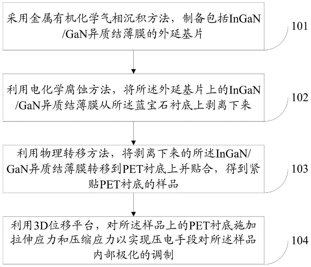
FIG. 1 is a schematic flow chart of a method for modulating internal polarization of an InGaN/GaN heterojunction film according to an embodiment of the present invention, as shown in FIG. 1, the method includes the following steps:
step 101: preparing an epitaxial substrate comprising an InGaN/GaN heterojunction film by adopting a metal organic chemical vapor deposition method; the epitaxial substrate comprises a sapphire substrate, and a first undoped GaN layer, a heavily doped n-GaN layer, a lightly doped n-GaN layer, a second undoped GaN layer, an InGaN quantum well layer and a p-GaN layer which are sequentially grown on the sapphire substrate.
Step 102: and stripping the InGaN/GaN heterojunction thin film on the epitaxial substrate from the sapphire substrate by using an electrochemical corrosion method.
Step 103: and transferring the stripped InGaN/GaN heterojunction film onto a PET substrate by using a physical transfer method and attaching to obtain a sample tightly attached to the PET substrate.
Step 104: and applying tensile stress and compressive stress to the PET substrate on the sample by using a 3D displacement platform so as to realize modulation of internal polarization of the sample by a piezoelectric means.
In step 101, the thickness of the first undoped GaN layer is 1.5um, the thickness of the heavily doped n-GaN layer is 2.5um, the thickness of the lightly doped n-GaN layer is 200nm, the thickness of the second undoped GaN layer is 3um, the thickness of the InGaN quantum well layer is 10nm, and the thickness of the p-GaN layer is 250 nm.
The heavily doped n-GaN layer is doped with Si with a doping concentration of 1.3 × 1019cm-3(ii) a The lightly doped n-GaN layer is doped with Si with a doping concentration of 2.2 × 1018cm-3。
The p-GaN layer is doped with Mg; the InGaN quantum well layer is a 1-cycle InGaN quantum well layer.
Step 102 specifically includes:
an oxalic acid electrolytic solution is prepared.
And coating silver paste on the heavily doped n-GaN layer of the epitaxial substrate.
One side of the epitaxial substrate coated with silver paste was connected to the Pt electrode with a clip as the anode for electrochemical corrosion, and the other Pt electrode was used as the cathode for electrochemical corrosion.
And connecting the anode, the oxalic acid electrolytic solution, the cathode and the direct current power supply in series to form a closed loop.
And adjusting the voltage and the corrosion time of the direct current power supply to strip the InGaN/GaN heterojunction thin film on the epitaxial substrate from the sapphire substrate.
Preferably, the concentration range of the oxalic acid electrolytic solution is 0.3-0.5 mol/L, the voltage range of the direct current power supply is 18-25V, and the corrosion time range is 20-30 min.
Step 103 specifically comprises: and transferring the stripped InGaN/GaN heterojunction film onto a PET substrate cleaned by plasma by using a transparent adhesive tape, and bonding the InGaN/GaN heterojunction film together to obtain a sample tightly attached to the PET substrate.
Step 104 specifically includes: building a test platform; the test platform comprises a laser, a 3D displacement platform, an optical filter, a focusing mirror, an optical fiber and a spectrum analyzer; light emitted by the laser is emitted onto a sample of the 3D displacement platform, photoluminescence excited on the sample sequentially enters the optical filter and the focusing mirror, is collected by the optical fiber and is finally transmitted into the spectrum analyzer.
Placing the sample on the 3D displacement stage.
The laser is turned on.
And applying tensile stress and compressive stress to the PET substrate on the sample by using the 3D displacement platform, irradiating the InGaN/GaN heterojunction film sample by using laser emitted by the laser, passing through the built light path, and finally forming a photoluminescence spectrum on the spectrum analyzer.
And analyzing photoluminescence spectra of the sample under different stresses, and carrying out piezoelectric modulation on the polarization inside the sample according to the analysis result.
The embodiment relates to the preparation of an InGaN/GaN heterojunction thin film and a process for piezoelectric modulation of internal piezoelectric polarization thereof. Specifically, the method comprises the steps of growing and peeling an InGaN/GaN heterojunction thin film and modulating internal polarization of the InGaN/GaN heterojunction thin film through piezoelectricity, the InGaN/GaN heterojunction thin film epitaxially grown on a sapphire substrate is peeled off at low cost and is transferred to a flexible PET substrate, a 3D displacement platform is used for applying compressive stress and tensile stress to the InGaN/GaN heterojunction thin film, and the modulation of external stress on the internal piezoelectric polarization of the InGaN/GaN heterojunction thin film is achieved at low cost and easily operated through measurement and analysis of photoluminescence spectra of the InGaN/GaN heterojunction thin film. The method provided by the embodiment has the advantages of extremely low cost, simplicity in operation, high repeatability and the like, and has a wide application prospect in the aspect of improving the efficiency of the LED in the future.
Example 2
The embodiment provides a method for modulating the internal polarization of an InGaN/GaN heterojunction film, which comprises the growth, stripping, transfer and piezoelectric modulation processes of the InGaN/GaN heterojunction film.
The growth process of the InGaN/GaN heterojunction thin film specifically comprises the following steps:
the sapphire is taken as a growth substrate, and an epitaxial substrate comprising an InGaN/GaN heterojunction film is prepared by adopting a metal organic chemical vapor deposition method. As shown in fig. 2, the epitaxial substrate includes a sapphire substrate 1, and a first undoped GaN layer 2, a heavily doped n-GaN layer 3, a lightly doped n-GaN layer 4, a second undoped GaN layer 5, an InGaN quantum well layer 6, and a p-GaN layer 7 sequentially grown on the sapphire substrate 1.
The actual operation process is as follows: the sapphire substrate 1 is loaded into a reaction chamber of a metal organic chemical vapor deposition system, and then a first undoped GaN layer 2 with a thickness of 1 μm, a heavily doped n-GaN layer 3 with a thickness of 2.5 μm, a lightly doped n-GaN layer 4 with a thickness of 200nm, a second undoped GaN layer 5 with a thickness of 3 μm, an InGaN quantum well layer 6 with a thickness of 10nm, and a p-GaN layer 7 with a thickness of 250nm are sequentially grown according to an epitaxial structure shown in fig. 2.
The stripping process is as follows: and stripping the InGaN/GaN heterojunction film growing on the heavily doped n-GaN layer 3 by adopting an electrochemical corrosion method.
The actual operation process is as follows: preparing oxalic acid electrolyte with the concentration of 0.3 mol/L.
And cutting the grown epitaxial substrate into 4mm multiplied by 10mm slices, cleaning the slices by acetone, isopropanol and deionized water, drying the slices by nitrogen, and finally baking the slices on a hot table for 5min to remove water molecules on the surface.
One end of the cut substrate was scribed with a diamond stylus into positive stripes of 2mm x 2mm or 1mm x 1mm to expose the heavily doped n-GaN layer 3.
The heavily doped n-GaN layer 3 is coated with silver paste, and the silver paste is left for a few minutes to form an electrode after solidification.
One side of the substrate coated with silver paste was connected to a Pt electrode with a clip as an anode for electrochemical corrosion, and the other Pt electrode was used as a cathode for electrochemical corrosion.
A direct current power supply, a substrate packaged by silver paste, a Pt sheet cathode and 0.3-0.5 mol/L oxalic acid electrolyte are connected in series to form a closed loop.
And adjusting the direct current power supply to enable the voltage of the direct current power supply to be 25V and the etching time to be 20min, wherein the etching process is shown in figure 3, and finally the InGaN/GaN heterojunction film on the epitaxial substrate is stripped from the sapphire substrate.
In the actual operation process, the epitaxial substrate, the Pt sheet cathode, the direct current power supply and the oxalic acid electrolyte packaged by the silver paste are connected in series through the conducting wires to form a closed loop, and the epitaxial substrate, the Pt sheet cathode, the direct current power supply and the oxalic acid electrolyte packaged by the silver paste are packaged into a whole.
The transfer process is as follows: the InGaN/GaN heterojunction film and the sapphire substrate are separated by the transparent adhesive tape and transferred onto the PET substrate, so that the stripped InGaN/GaN heterojunction film is attached to the PET substrate, namely, the InGaN/GaN heterojunction film is not separated from the PET substrate when stress is applied.
The actual operation process is as follows: the etched substrate was placed under a microscope.
The transparent adhesive tape was cut into stripes of 0.1mm X1 cm.
The cut transparent adhesive tape is lightly placed at the upper end of the corroded substrate, and the InGaN/GaN heterojunction thin film which is completely separated from the sapphire substrate, namely the InGaN/GaN heterojunction thin film above the heavily doped n-GaN layer 3 can be separated from the original substrate, is collected by using the principle of electrostatic attraction of small objects.
The InGaN/GaN heterojunction film was transferred under a microscope onto a flexible PET substrate that had been cleaned with oxygen plasma using a 0.1mm by 1cm transparent tape and bonded together.
In this example, the area of the flexible PET substrate was 2cm2。
The piezoelectric modulation process is as follows: tensile stress and compressive stress are applied to a PET substrate containing the InGaN/GaN heterojunction thin film through a 3D displacement platform (because the Young modulus of the PET substrate is larger, the force applied to the PET substrate is applied to the InGaN/GaN heterojunction thin film), and then photoluminescence spectrums of the InGaN/GaN heterojunction thin film under different stresses are collected.
The actual operation process is as follows:
building a piezoelectric test light path as shown in FIG. 4; the piezoelectric testing optical path comprises a 325nm He-Cd laser 11, two large and constant photoelectric 3D displacement platforms 12, a 400nm optical filter 13, a convex lens 14 with the focal length of 5cm and a spectrometer 15 with the model of Maya Pro 2000. In fig. 4, the black line indicates the path of the laser beam.
The two 3D stages 12 were calibrated to zero and a PET substrate 16 containing an InGaN/GaN heterojunction thin film was placed on the two 3D stages 12.
And opening the He-Cd laser 11 and preheating for 10-15 min.
Adjusting two 3D displacement platforms 12 to deform a PET substrate 16 containing an InGaN/GaN heterojunction film, irradiating the InGaN/GaN heterojunction film with laser emitted by a 325nm He-Cd laser 11 to make the InGaN/GaN heterojunction film photoluminescence, focusing the emitted fluorescence by using a focusing mirror 14, and finally collecting the emitted fluorescence by using a spectrometer 15 of Maya Pro 2000 model to generate a photoluminescence spectrum.
The two 3D stages 12 were adjusted to deform the PET substrate 16 containing the InGaN/GaN heterojunction thin film differently, and the above operation was repeated.
In the present embodiment, each of the 3D stages 12 is a manual stage, and is mounted at both ends of the PET substrate 16 including the InGaN/GaN heterojunction thin film, and is capable of simultaneously applying stress (including compressive stress and tensile stress) to the PET substrate 16 including the InGaN/GaN heterojunction thin film. Wherein the stress applied to the PET substrate 16 containing the InGaN/GaN heterojunction thin film is in the range of 0-0.4%, and cannot be too large, which may cause the PET substrate to crack.
In the test of applying 0-0.4% compressive stress and tensile stress to the PET substrate 16 including the InGaN/GaN heterojunction thin film, the magnitude of the applied stress was calculated by adjusting the axial travel distance of XYZ axes on the 3D stage 12.
The 325nm He-Cd laser 11 comprises a PET substrate 16 of an InGaN/GaN heterojunction film, two 3D displacement platforms 12, a 400nm optical filter 13, a convex lens 14 with the focal length of 5cm, and a spectrometer 15 of Maya Pro 2000 type, and is packaged into a whole.
The piezoelectric testing optical path built by the embodiment is relatively simple and low in cost, but can be used for efficiently measuring the obvious change of PL light intensity caused by the modulation of the internal polarization of the InGaN/GaN heterojunction thin film by the piezoelectric.
The experimental results are shown in fig. 5-6, the PL light intensity is changed by 600% before and after under the action of compressive stress, the PL light intensity is changed by 800% before and after under the action of tensile stress, and the piezoelectric polarization effect is obvious. Reflecting the difference between the front and back photoluminescence intensities of the InGaN/GaN heterojunction film under different stresses. The intensity of photoluminescence is strongly related to the modulation of internal polarization, and if the tensile stress applied along the c-axis is increased and the externally induced polarization is in the same direction as the polarization inside InGaN, the carrier recombination efficiency in InGaN is reduced and the intensity of photoluminescence is reduced. On the contrary, under the action of compressive stress, the polarization caused by external application is opposite to the polarization direction in the InGaN, so that the carrier recombination efficiency in the InGaN is increased, and the photoluminescence intensity is increased. Of course, if too much compressive stress is applied, lattice scattering inside GaN will also cause a decrease in photoluminescence intensity.
Example 3
On the basis of embodiment 2, molten In metal is placed on the position of the heavily doped n-GaN layer 3, and good ohmic contact can be formed between the heavily doped n-GaN layer 3 and the electrode Pt sheet, so that the carrier transport is enhanced.
Example 4
On the basis of the embodiment 2, the heavily doped n-GaN layer 3 is etched by a voltage transformation method, and the voltage range is 18-25V. Because the silver paste electrode is easy to fall off along with the progress of the corrosion reaction, the voltage is increased timely to be beneficial to the progress of the corrosion reaction, but the area of the obtained InGaN/GaN heterojunction film is larger when the voltage is slightly small.
Example 5
Based on example 2, in the test of applying 0-0.6% compressive stress and tensile stress to both ends of the PET substrate 16 containing the InGaN/GaN heterojunction thin film, the magnitude of the applied stress is calculated by adjusting XYZ axes on the 3D displacement stage 12 and by the distance traveled by the axes at both ends, and it is found that the magnitude of the stress should be optimally between 0-0.4%, and the measured photoluminescence intensity is sensitive to the magnitude of the strain.
The embodiments in the present description are described in a progressive manner, each embodiment focuses on differences from other embodiments, and the same and similar parts among the embodiments are referred to each other.
The principles and embodiments of the present invention have been described herein using specific examples, which are provided only to help understand the method and the core concept of the present invention; meanwhile, for a person skilled in the art, according to the idea of the present invention, the specific embodiments and the application range may be changed. In view of the above, the present disclosure should not be construed as limiting the invention.