CN111584760B - Display panel, preparation method of display panel and display device - Google Patents
Display panel, preparation method of display panel and display device Download PDFInfo
- Publication number
- CN111584760B CN111584760B CN202010467119.5A CN202010467119A CN111584760B CN 111584760 B CN111584760 B CN 111584760B CN 202010467119 A CN202010467119 A CN 202010467119A CN 111584760 B CN111584760 B CN 111584760B
- Authority
- CN
- China
- Prior art keywords
- layer
- array substrate
- frame glue
- encapsulation
- packaging frame
- Prior art date
- Legal status (The legal status is an assumption and is not a legal conclusion. Google has not performed a legal analysis and makes no representation as to the accuracy of the status listed.)
- Active
Links
Images


Classifications
-
- H—ELECTRICITY
- H10—SEMICONDUCTOR DEVICES; ELECTRIC SOLID-STATE DEVICES NOT OTHERWISE PROVIDED FOR
- H10K—ORGANIC ELECTRIC SOLID-STATE DEVICES
- H10K50/00—Organic light-emitting devices
- H10K50/80—Constructional details
- H10K50/84—Passivation; Containers; Encapsulations
- H10K50/842—Containers
- H10K50/8426—Peripheral sealing arrangements, e.g. adhesives, sealants
-
- H—ELECTRICITY
- H10—SEMICONDUCTOR DEVICES; ELECTRIC SOLID-STATE DEVICES NOT OTHERWISE PROVIDED FOR
- H10K—ORGANIC ELECTRIC SOLID-STATE DEVICES
- H10K59/00—Integrated devices, or assemblies of multiple devices, comprising at least one organic light-emitting element covered by group H10K50/00
- H10K59/10—OLED displays
-
- H—ELECTRICITY
- H10—SEMICONDUCTOR DEVICES; ELECTRIC SOLID-STATE DEVICES NOT OTHERWISE PROVIDED FOR
- H10K—ORGANIC ELECTRIC SOLID-STATE DEVICES
- H10K71/00—Manufacture or treatment specially adapted for the organic devices covered by this subclass
Landscapes
- Physics & Mathematics (AREA)
- Optics & Photonics (AREA)
- Engineering & Computer Science (AREA)
- Manufacturing & Machinery (AREA)
- Electroluminescent Light Sources (AREA)
Abstract
本发明涉及显示领域,公开一种显示面板、显示面板的制备方法及显示装置,该显示面板,包括:阵列基板和与阵列基板相对设置的封装层;阵列基板与封装层之间设有第一封装框胶和第二封装框胶,且阵列基板朝向封装层的表面设有发光结构层,其中:第一封装框胶和第二封装框胶位于阵列基板的边缘部位,且第一封装框胶和第二封装框胶均具有封闭环形结构,第一封装框胶和发光结构层位于第二封装框胶所围空间内,且发光结构层在阵列基板上的投影至少覆盖第一封装框胶在阵列基板上的投影;在第一封装框胶和第二封装框胶围成的区域内填充有填充胶;用于隔绝外部的水氧,提高显示面板的使用寿命。
The present invention relates to the display field, and discloses a display panel, a method for preparing the display panel, and a display device. The display panel includes: an array substrate and an encapsulation layer opposite to the array substrate; a first Encapsulating frame glue and second encapsulating frame glue, and the surface of the array substrate facing the encapsulation layer is provided with a light-emitting structure layer, wherein: the first encapsulating frame glue and the second encapsulating frame glue are located at the edge of the array substrate, and the first encapsulating frame glue and the second encapsulation sealant have a closed ring structure, the first encapsulation sealant and the light-emitting structure layer are located in the space enclosed by the second encapsulation sealant, and the projection of the light-emitting structure layer on the array substrate covers at least the first encapsulation sealant The projection on the array substrate; filling the area surrounded by the first encapsulation frame glue and the second encapsulation frame glue; used for isolating external water and oxygen, and improving the service life of the display panel.
Description
技术领域technical field
本发明涉及显示技术领域,特别涉及一种显示面板、显示面板的制备方法及显示装置。The invention relates to the field of display technology, in particular to a display panel, a method for preparing the display panel, and a display device.
背景技术Background technique
有机发光显示装置具有轻薄、主动发光、宽视角、快速响应、能耗低、低温和抗震性能优异以及可实现柔性显示等优点。有机发光显示装置中的有机发光器件(OLED)的发光结构层中的材料通常采用化学性质较为活泼的金属材质,上述金属材质容易与水氧发生反应,因为水氧容易与金属发生反应,使材料的光电特性改变,导致OLED器件失效。Organic light-emitting display devices have the advantages of thinness, active light emission, wide viewing angle, fast response, low energy consumption, excellent low temperature and shock resistance, and can realize flexible display. The material in the light-emitting structure layer of the organic light-emitting device (OLED) in the organic light-emitting display device is usually made of a metal material with relatively active chemical properties. The photoelectric characteristics of the OLED are changed, leading to the failure of the OLED device.
发明内容Contents of the invention
本发明公开了一种显示面板、显示面板的制备方法及显示装置,用于隔绝外部的水氧,提高显示面板的使用寿命。The invention discloses a display panel, a preparation method of the display panel and a display device, which are used for isolating external water and oxygen and improving the service life of the display panel.
为达到上述目的,本发明提供以下技术方案:To achieve the above object, the present invention provides the following technical solutions:
第一方面,本发明提供一种显示面板,包括:阵列基板和与所述阵列基板相对设置的封装层;In a first aspect, the present invention provides a display panel, comprising: an array substrate and an encapsulation layer disposed opposite to the array substrate;
所述阵列基板与所述封装层之间设有第一封装框胶和第二封装框胶,且所述阵列基板朝向所述封装层的表面设有发光结构层,其中:A first encapsulation sealant and a second encapsulation sealant are provided between the array substrate and the encapsulation layer, and a light-emitting structure layer is provided on the surface of the array substrate facing the encapsulation layer, wherein:
所述第一封装框胶和所述第二封装框胶位于所述阵列基板的边缘部位,且所述第一封装框胶和所述第二封装框胶均具有封闭环形结构,所述第一封装框胶和所述发光结构层位于所述第二封装框胶所围空间内,且所述发光结构层在所述阵列基板上的投影至少覆盖所述第一封装框胶在所述阵列基板上的投影;The first packaging sealant and the second packaging sealant are located at the edge of the array substrate, and both the first packaging sealant and the second packaging sealant have a closed ring structure, and the first The packaging sealant and the light-emitting structure layer are located in the space surrounded by the second packaging sealant, and the projection of the light-emitting structure layer on the array substrate at least covers the first packaging sealant on the array substrate projection on
在所述第一封装框胶和所述第二封装框胶围成的区域内填充有填充胶。The area enclosed by the first encapsulation sealant and the second encapsulation sealant is filled with filler.
通过在阵列基板与封装层之间设有第一封装框胶和第二封装框胶,加强封装层和阵列基板之间的连接,通过设置多个封装胶框达到了良好的阻隔效果,在阵列基板朝向封装层的表面设有发光结构层,第一封装框胶和第二封装框胶位于阵列基板的边缘部位,这里第一封装框胶和所述第二封装框胶均具有封闭环形结构,并在围成的空间中填充有填充胶,起到支撑和减缓水氧渗透进入发光结构层的效果;但是封装框胶过多会占据了额外的宽度,增加了边框宽度,即增加了封装层边缘至或发光结构层边缘的距离,为了在保证减缓水氧渗透效果的同时又不会增加边框的宽度,这里将发光结构层在阵列基板上的投影至少覆盖第一封装框胶在阵列基板上的投影。By setting the first packaging sealant and the second packaging sealant between the array substrate and the packaging layer, the connection between the packaging layer and the array substrate is strengthened, and a good barrier effect is achieved by setting multiple packaging plastic frames. In the array The surface of the substrate facing the encapsulation layer is provided with a light-emitting structure layer, and the first encapsulation sealant and the second encapsulation sealant are located at the edge of the array substrate, where the first encapsulation sealant and the second encapsulation sealant both have a closed ring structure, And the enclosed space is filled with filling glue to support and slow down the penetration of water and oxygen into the light-emitting structure layer; but too much encapsulation frame glue will occupy additional width, increasing the frame width, that is, increasing the encapsulation layer The distance from the edge to or the edge of the light-emitting structure layer, in order to ensure the effect of slowing down the penetration of water and oxygen without increasing the width of the frame, here the projection of the light-emitting structure layer on the array substrate at least covers the first encapsulation sealant on the array substrate projection.
进一步地,所述第一封装框胶包括:设置于所述阵列基板朝向所述封装层一侧表面的第一子封装框胶;Further, the first encapsulation sealant includes: a first sub-encapsulation sealant disposed on the surface of the array substrate facing the encapsulation layer;
设置于所述封装层朝向所述阵列基板一侧表面的第二子封装框胶;a second sub-encapsulation sealant disposed on the surface of the encapsulation layer facing the array substrate;
所述发光结构层的边缘覆盖所述第一子封装框胶朝向所述第二子封装框胶的表面。The edge of the light-emitting structure layer covers the surface of the first sub-encapsulation sealant facing the second sub-encapsulation sealant.
进一步地,所述阵列基板朝向所述封装层的一侧设有至少两个凸起结构,其中:Further, at least two protrusion structures are provided on the side of the array substrate facing the encapsulation layer, wherein:
一个所述凸起结构位于所述第一封装框胶所围区域内;One of the raised structures is located in the area surrounded by the first encapsulation sealant;
另一个所述凸起结构位于所述第一封装框胶和第二封装框胶之间。The other protruding structure is located between the first encapsulation sealant and the second encapsulation sealant.
进一步地,所述发光结构层包括有机电致发光器件层、以及位于所述有机电致发光器件层朝向所述封装层一侧的钝化层,所述有机电致发光器件层包括阴极、位于所述阴极背离阵列基板一侧的电致发光层、以及位于所述电致发光层背离所述阴极一侧的阳极;Further, the light-emitting structure layer includes an organic electroluminescent device layer, and a passivation layer located on the side of the organic electroluminescent device layer facing the encapsulation layer, and the organic electroluminescent device layer includes a cathode, located on the The electroluminescent layer on the side of the cathode away from the array substrate, and the anode on the side of the electroluminescent layer away from the cathode;
所述电致发光层和所述阴极层在所述凸起结构处断开。The electroluminescent layer and the cathode layer are disconnected at the raised structure.
进一步地,所述凸起结构为倒梯形或矩形。Further, the raised structure is an inverted trapezoid or a rectangle.
进一步地,所述凸起结构的材料为无机材料、钛铝合金和感光树脂的其中一种或多种。Further, the material of the protrusion structure is one or more of inorganic materials, titanium aluminum alloy and photosensitive resin.
进一步地,所述发光结构层包括有机电致发光器件层、以及位于所述有机电致发光器件层朝向封装层一侧的钝化层;Further, the light-emitting structure layer includes an organic electroluminescent device layer, and a passivation layer located on the side of the organic electroluminescent device layer facing the encapsulation layer;
所述钝化层延伸至所述第一封装框胶与所述第二封装框胶之间,所述有机电致发光器件层位于所述第一封装框胶所围区域内。The passivation layer extends between the first encapsulation sealant and the second encapsulation sealant, and the organic electroluminescent device layer is located in the area surrounded by the first encapsulation sealant.
进一步地,所述钝化层和所述有机电致发光器件层均延伸至所述第一封装框胶与所述第二封装框胶之间。Further, both the passivation layer and the organic electroluminescent device layer extend between the first encapsulation sealant and the second encapsulation sealant.
进一步地,所述第一封装框胶和第二封装框胶的材料为:聚亚酰胺或丙烯酸。Further, the material of the first encapsulation sealant and the second encapsulation sealant is polyimide or acrylic.
第二方面,本发明提供的一种显示装置,包括:第一方面任一项所述的显示面板。In a second aspect, the present invention provides a display device, comprising: the display panel described in any one of the first aspect.
第三方面,本发明提供的一种显示面板的制备方法,包括:阵列基板和与所述阵列基板相对设置的封装层;In a third aspect, the present invention provides a method for manufacturing a display panel, comprising: an array substrate and an encapsulation layer disposed opposite to the array substrate;
所述阵列基板与所述封装层之间形成有第一封装框胶和第二封装框胶,且所述阵列基板朝向所述封装层的表面形成有发光结构层,其中:A first encapsulation sealant and a second encapsulation sealant are formed between the array substrate and the encapsulation layer, and a light-emitting structure layer is formed on the surface of the array substrate facing the encapsulation layer, wherein:
所述第一封装框胶和所述第二封装框胶位于所述阵列基板的边缘部位,且所述第一封装框胶和所述第二封装框胶均具有封闭环形结构,所述第一封装框胶和所述发光结构层位于所述第二封装框胶所围空间内,且所述发光结构层在所述阵列基板上的投影至少覆盖所述第一封装框胶在所述阵列基板上的投影;The first packaging sealant and the second packaging sealant are located at the edge of the array substrate, and both the first packaging sealant and the second packaging sealant have a closed ring structure, and the first The packaging sealant and the light-emitting structure layer are located in the space surrounded by the second packaging sealant, and the projection of the light-emitting structure layer on the array substrate at least covers the first packaging sealant on the array substrate projection on
在所述第一封装框胶和所述第二封装框胶围成的区域内填充有填充胶。The area enclosed by the first encapsulation sealant and the second encapsulation sealant is filled with filler.
第二方面和第三方面中所带来的技术效果可参见第一方面中对应的技术效果,此处不再赘述。For the technical effects brought by the second aspect and the third aspect, please refer to the corresponding technical effects in the first aspect, which will not be repeated here.
附图说明Description of drawings
图1为本发明实施例提供的发光结构层未穿过封装框胶的结构示意图;Fig. 1 is a schematic structural view of the light-emitting structure layer provided by the embodiment of the present invention without passing through the encapsulation sealant;
图2为本发明实施例提供的一种显示面板的结构示意图;FIG. 2 is a schematic structural diagram of a display panel provided by an embodiment of the present invention;
图3为本发明实施例提供的另一种显示面板的结构示意图;FIG. 3 is a schematic structural diagram of another display panel provided by an embodiment of the present invention;
图4为本发明实施例提供的另一种显示面板的结构示意图;FIG. 4 is a schematic structural diagram of another display panel provided by an embodiment of the present invention;
图5为本发明实施例提供的另一种显示面板的结构示意图;FIG. 5 is a schematic structural diagram of another display panel provided by an embodiment of the present invention;
图6为本发明实施例提供的另一种显示面板的结构示意图。FIG. 6 is a schematic structural diagram of another display panel provided by an embodiment of the present invention.
图标:100-阵列基板;200-封装层;300-第一封装框胶;310-第一子封装框胶;320-第二子封装框胶;400-第二封装框胶;500-发光结构层;510-有机电致发光器件层;520-钝化层;600-填充胶;700-凸起结构。Icon: 100-array substrate; 200-encapsulation layer; 300-first package frame glue; 310-first sub-package frame glue; 320-second sub-package frame glue; 400-second package frame glue; 500-luminescent structure layer; 510—organic electroluminescent device layer; 520—passivation layer; 600—filling glue; 700—protruding structure.
具体实施方式detailed description
下面将结合本发明实施例中的附图,对本发明实施例中的技术方案进行清楚、完整地描述,显然,所描述的实施例仅仅是本发明一部分实施例,而不是全部的实施例。基于本发明中的实施例,本领域普通技术人员在没有做出创造性劳动前提下所获得的所有其他实施例,都属于本发明保护的范围。The following will clearly and completely describe the technical solutions in the embodiments of the present invention with reference to the accompanying drawings in the embodiments of the present invention. Obviously, the described embodiments are only some, not all, embodiments of the present invention. Based on the embodiments of the present invention, all other embodiments obtained by persons of ordinary skill in the art without making creative efforts belong to the protection scope of the present invention.
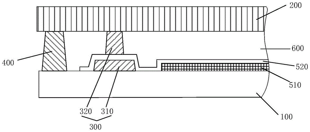
封装框胶,如图1中的第一封装框胶300和第二封装框胶400,过多会占据了额外的宽度,增加了边框宽度a,即增加了封装层200边缘至或发光结构层500边缘的距离,为了在保证减缓水氧渗透效果的同时又不会增加边框的宽度,这里将发光结构层500在阵列基板100上的投影至少覆盖第一封装框胶300在发光结构层500的投影。Encapsulation sealant, such as the
如图2所示,第一方面,本发明实施例提供了一种显示面板,包括:阵列基板100和与阵列基板100相对设置的封装层200;As shown in FIG. 2 , in a first aspect, an embodiment of the present invention provides a display panel, including: an
阵列基板100与封装层200之间设有第一封装框胶300和第二封装框胶400,且阵列基板100朝向封装层200的表面设有发光结构层500,其中:A
第一封装框胶300和第二封装框胶400位于阵列基板100的边缘部位,且第一封装框胶300和第二封装框胶400均具有封闭环形结构,第一封装框胶300和发光结构层500位于第二封装框胶400所围空间内,且发光结构层500在阵列基板100上的投影至少覆盖第一封装框胶300在阵列基板100的投影;在第一封装框胶300和第二封装框胶400围成的区域内填充有填充胶600。The
需要说明的是,通过在阵列基板100与封装层200之间设有第一封装框胶300和第二封装框胶400,加强封装层200和阵列基板100之间的连接,通过设置多个封装胶框达到了良好的阻隔效果,在阵列基板100朝向封装层200的表面设有发光结构层500,第一封装框胶300和第二封装框胶400位于阵列基板100的边缘部位,这里第一封装框胶300和所述第二封装框胶400均具有封闭环形结构,并在围成的空间中填充有填充胶600,起到支撑和减缓水氧渗透进入发光结构层500的效果。It should be noted that by providing the
具体地,第一封装框胶300包括:设置于阵列基板100朝向封装层200一侧表面的第一子封装框胶310;Specifically, the
以及,设置于封装层200朝向阵列基板100一侧表面的第二子封装框胶320;And, the
发光结构层500的边缘覆盖第一子封装框胶310朝向第二子封装框胶320的表面。The edge of the light
通过上下设置封装框胶方法,第一封装框胶300由第一子封装框胶310和第二子封装框胶320形成,使得发光结构层500可以与第一封装框胶300交叠,形成发光结构层500穿过框胶的效果,减缓了水氧向内的渗透,这样既增强了封装阻隔效果,又不显著增加边框。By setting the encapsulation sealant up and down, the
如图3所示,阵列基板100朝向封装层200的一侧设有至少两个凸起结构700,其中:一个凸起结构700位于第一封装框胶300所围区域内;As shown in FIG. 3 , at least two
另一个凸起结构700位于第一封装框胶300和第二封装框胶400之间。Another
上述凸起结构700有多种选择方式:There are many options for the above-mentioned raised structure 700:
方式一,凸起结构700为倒梯形。Mode 1, the
通过在第一封装框胶300所围区域内和第一封装框胶300所围区域的外侧设置多圈凸起结构700,此外在多圈倒梯形结构之间设置多圈封装框胶,尤其设置了从上下夹住发光结构层500的第一子封装框胶310和第二子封装框胶320,进一步地阻挡了水氧穿过带有倒梯形结构的区域。By arranging a multi-circle
在OLED发光结构层500制作中,发光结构层500位于第二封装框胶400朝向阵列基板100的一侧,可以不考虑显示屏的形状,采用规则的矩形开口掩膜,简单的控制工艺,在阵列基板100上制作矩形图样的膜层。In the manufacture of the OLED light-emitting
在边缘封装区域,制作OLED发光结构层500时,发光结构层500位于第二封装框胶400朝向阵列基板100的一侧,而第一封装框胶300设置了从上下夹住发光结构层500的第一子封装框胶310和第二子封装框胶320,由于凸起结构700为倒梯形,OLED发光结构层500在倒梯形的凸起结构的顶端和底部,因高度差而断开,在倒梯形结构所围成区域内,形成显示区域,并隔绝水氧沿着发光结构层500向内渗透的途径。In the edge encapsulation area, when making the OLED light-emitting
如图4所示,具体的发光结构层500包括有机电致发光器件层510、以及位于有机电致发光器件层510朝向封装层200一侧的钝化层520,通过在有机电致发光器件层510上设置有钝化层520,更好的隔绝水氧向有机发光致电层510的渗透;有机电致发光器件层510包括阴极、位于阴极背离阵列基板100一侧的电致发光层、以及位于电致发光层背离阴极一侧的阳极;电致发光层和阴极层在凸起结构700处断开。As shown in FIG. 4 , the specific light-emitting
方式二,凸起结构700为矩形。Mode 2, the protruding
通过在第一封装框胶300所围区域内和第一封装框胶300所围区域的外侧设置多圈凸起结构700,此外在多圈矩形结构之间设置多圈封装框胶,尤其设置了从上下夹住发光结构层500的第一子封装框胶310和第二子封装框胶320,进一步地阻挡了水氧穿过带有矩形结构的区域。By arranging a multi-circle
在OLED发光结构层500制作中,发光结构层位于第二封装框胶朝向阵列基板的一侧,可以不考虑显示屏的形状,采用规则的矩形开口掩膜,简单的控制工艺,在阵列基板100上制作矩形图样的膜层。In the manufacture of the OLED light-emitting
在边缘封装区域,制作OLED发光结构层500时,发光结构层500位于第二封装框胶朝向阵列基板100的一侧,而第一封装框胶设置了从上下夹住发光结构层500的第一子封装框胶310和第二子封装框胶320,由于凸起结构700为矩形,OLED发光结构层500在矩形的凸起结构的顶端和底部,因高度差而断开,在矩形结构所围成区域内,形成显示区域,并隔绝水氧沿着发光结构层500向内渗透的途径。In the edge encapsulation area, when making the OLED light-emitting
如图4所示,具体的发光结构层500包括有机电致发光器件层510、以及位于有机电致发光器件层510朝向封装层200一侧的钝化层520,通过在有机电致发光器件层510上设置有钝化层520,更好的隔绝水氧向有机电致发光器件层510的渗透;有机电致发光器件层510包括阴极、位于阴极背离阵列基板100一侧的电致发光层、以及位于电致发光层背离阴极一侧的阳极;电致发光层和阴极层在凸起结构700处断开。As shown in FIG. 4 , the specific light-emitting
具体地,凸起结构700的材料为氮化硅氧化硅等无机材料,钛铝合金等多层金属,通过化学和物理沉积后,通过湿法和干法刻蚀形成。Specifically, the material of the protruding
另外,倒梯形结构的材料还可以是感光树脂,通过一次或多次曝光显影并固化成形。In addition, the material of the inverted trapezoidal structure can also be a photosensitive resin, which is developed and cured by one or more exposures.
如图5所示,阵列基板100和与阵列基板100相对设置的封装层200;阵列基板100与封装层200之间设有第一封装框胶300和第二封装框胶400,且阵列基板100朝向封装层200的表面设有发光结构层500,发光结构层500将第一封装框胶300分成第一子封装框胶310和第二子封装框胶320,具体的发光结构层500包括有机电致发光器件层510、以及位于有机电致发光器件层510朝向封装层200一侧的钝化层520。As shown in FIG. 5, the
钝化层520材料是氮化硅,金属氧化物,用化学或物理沉积的工艺制作,成膜区域与有机电致发光器件层510一致,以共用掩膜。The material of the
钝化层520延伸至第一封装框胶300与第二封装框胶400之间,有机电致发光器件层510位于第一封装框胶400所围区域内。The
如图6所示,阵列基板100和与阵列基板100相对设置的封装层200;阵列基板100与封装层200之间设有第一封装框胶300和第二封装框胶400,且阵列基板100朝向封装层200的表面设有发光结构层500,发光结构层500将第一封装框胶300分成第一子封装框胶310和第二子封装框胶320,具体的发光结构层500包括有机电致发光器件层510、以及位于有机电致发光器件层510朝向封装层200一侧的钝化层520。As shown in FIG. 6, the
钝化层520和有机电致发光器件层510在阵列基板100上的投影均至少覆盖第一封装框胶300在阵列基板100上的投影,有机电致发光器件层510位于第一封装框胶300围成的区域内,和位于第一子封装框胶310和第二子封装框胶320之间,并且钝化层520覆盖有机发光电致发光器件层510并延伸到第一封装框胶300和第二封装框胶400之间。The projections of the
另外,第一封装框胶300和第二封装框胶400的材料是紫外线固化或热固化的,丙烯酸类,聚亚酰胺类有机材料;通过针头涂布,打印等工艺在相应位置涂布后再固化成形。In addition, the materials of the
上述第一封装框胶300中的第一子封装框胶310还可以是氮化硅,氧化硅,相对不活泼的金属,如钼,钛等,通过化学和物理沉积,在通过干法或湿法刻蚀,在阵列基板100边缘相应区域形成所需的图形。The
第一子封装框胶310和第二子封装框胶320可以是添加了氧化钙等吸水性材料的丙烯酸类等有机材料,通过水的吸水,进一步减缓水汽向内的渗透。The first
第二方面,本发明实施例提供的一种显示装置,包括:第一方面任一项的显示面板。In a second aspect, a display device provided by an embodiment of the present invention includes: the display panel according to any one of the first aspect.
第三方面,本发明实施例提供的一种显示面板的制备方法,包括:阵列基板100和与阵列基板100相对设置的封装层200;In a third aspect, a method for manufacturing a display panel provided by an embodiment of the present invention includes: an
阵列基板100与封装层200之间形成有第一封装框胶300和第二封装框胶400,且阵列基板100朝向封装层200的表面形成有发光结构层500,其中:A
第一封装框胶300和第二封装框胶400位于阵列基板100的边缘部位,且第一封装框胶300和第二封装框胶400均具有封闭环形结构,第一封装框胶300和发光结构层500位于第二封装框胶400所围空间内,且发光结构层500在阵列基板100上的投影至少覆盖第一封装框胶300在阵列基板100上的投影;The
在第一封装框胶300和第二封装框胶400围成的区域内填充有填充胶600。The area surrounded by the
如图5和图6所示,关于显示面板的制备过程具有如下两种方式:As shown in FIG. 5 and FIG. 6, there are two methods for the preparation process of the display panel as follows:
方式一,阵列基板100与封装层200相对设置,在阵列基板100朝向封装层200的一侧形成凸起结构700,在阵列基板100和封装层200之间先形成第一封装框胶300中的第一子封装框胶310,而后在阵列基板100朝向封装层200的表面形成有发光结构层500中的有机电致发光器件层510,然后在有机电致发光器件层510的朝向封装层200的一侧形成有钝化层520,在钝化层520朝向封装层200的一侧形成有第二子封装框胶320,实现了第二子封装框胶320与封装层200的贴合,在阵列基板100的边缘部位,形成有第二封装框胶400,之后在第一封装框胶300和第二封装框胶400围成的区域内填充有填充胶600,使得封装层200和阵列基板100贴合;这里从在阵列基板100和封装层200之间制作第一封装框胶300中的第一子封装框胶310开始,选择在干燥的空气,真空或无水氧气氛的工艺环境中进行后面其他步骤的制作。Method 1: The
方式二,阵列基板100与封装层200相对设置,在阵列基板100朝向封装层200的一侧形成凸起结构700,在阵列基板100和封装层200之间先形成有发光结构层500中的有机电致发光器件层510,而后在有机电致发光器件层510上形成第一封装框胶300中的第一子封装框胶310,然后在有机电致发光器件层510的朝向封装层200的一侧形成有钝化层520,在钝化层520朝向封装层200的一侧形成有第二子封装框胶320,实现了第二子封装框胶320与封装层200的贴合,在阵列基板100的边缘部位,形成有第二封装框胶400,之后在第一封装框胶300和第二封装框胶400围成的区域内填充有填充胶600,使得封装层200和阵列基板100贴合;这里从在阵列基板100和封装层200之间制作第一封装框胶300中的第一子封装框胶310开始,选择在干燥的空气,真空或无水氧气氛的工艺环境中进行制作。Method 2: The
显然,本领域的技术人员可以对本发明实施例进行各种改动和变型而不脱离本发明的精神和范围。这样,倘若本发明的这些修改和变型属于本发明权利要求及其等同技术的范围之内,则本发明也意图包含这些改动和变型在内。Apparently, those skilled in the art can make various changes and modifications to the embodiments of the present invention without departing from the spirit and scope of the present invention. Thus, if these modifications and variations of the present invention fall within the scope of the claims of the present invention and their equivalent technologies, the present invention also intends to include these modifications and variations.
Claims (10)
Priority Applications (1)
| Application Number | Priority Date | Filing Date | Title |
|---|---|---|---|
| CN202010467119.5A CN111584760B (en) | 2020-05-28 | 2020-05-28 | Display panel, preparation method of display panel and display device |
Applications Claiming Priority (1)
| Application Number | Priority Date | Filing Date | Title |
|---|---|---|---|
| CN202010467119.5A CN111584760B (en) | 2020-05-28 | 2020-05-28 | Display panel, preparation method of display panel and display device |
Publications (2)
| Publication Number | Publication Date |
|---|---|
| CN111584760A CN111584760A (en) | 2020-08-25 |
| CN111584760B true CN111584760B (en) | 2023-01-13 |
Family
ID=72112688
Family Applications (1)
| Application Number | Title | Priority Date | Filing Date |
|---|---|---|---|
| CN202010467119.5A Active CN111584760B (en) | 2020-05-28 | 2020-05-28 | Display panel, preparation method of display panel and display device |
Country Status (1)
| Country | Link |
|---|---|
| CN (1) | CN111584760B (en) |
Families Citing this family (2)
| Publication number | Priority date | Publication date | Assignee | Title |
|---|---|---|---|---|
| CN113782556A (en) * | 2021-09-10 | 2021-12-10 | 深圳市华星光电半导体显示技术有限公司 | A method for manufacturing a display panel, a method for manufacturing a splicing screen, and a display device |
| WO2026065319A1 (en) * | 2024-09-29 | 2026-04-02 | 京东方科技集团股份有限公司 | Light-emitting substrate and preparation method therefor, and light-emitting apparatus |
Family Cites Families (3)
| Publication number | Priority date | Publication date | Assignee | Title |
|---|---|---|---|---|
| US11042054B2 (en) * | 2018-09-30 | 2021-06-22 | HKC Corporation Limited | Display panel and display device |
| CN109935730B (en) * | 2019-03-28 | 2021-10-26 | 京东方科技集团股份有限公司 | Display substrate, preparation method thereof and display device |
| CN110429207B (en) * | 2019-08-07 | 2022-06-03 | 合肥鑫晟光电科技有限公司 | Display panel, display device and manufacturing method |
-
2020
- 2020-05-28 CN CN202010467119.5A patent/CN111584760B/en active Active
Also Published As
| Publication number | Publication date |
|---|---|
| CN111584760A (en) | 2020-08-25 |
Similar Documents
| Publication | Publication Date | Title |
|---|---|---|
| US12349588B2 (en) | OLED edge reinforcement holes and forming method | |
| CN108198953B (en) | OLED encapsulation method and OLED encapsulating structure | |
| WO2019041946A1 (en) | Display substrate and manufacturing method therefor, and display device | |
| JP2020531885A (en) | Display board and its manufacturing method, display panel | |
| WO2018214962A1 (en) | Package structure of organic light emitting diode display panel and manufacturing method thereof, and display device | |
| WO2020155441A1 (en) | Display panel and display device | |
| CN113299702B (en) | Display panel and preparation method thereof | |
| WO2020151048A1 (en) | Light-emitting panel, preparation method thereof, and display device | |
| CN110993819A (en) | Display panel and method of making the same | |
| CN111584760B (en) | Display panel, preparation method of display panel and display device | |
| CN110993813A (en) | OLED display panel and preparation method thereof | |
| WO2017161628A1 (en) | Packaging method for oled substrate and oled packaging structure | |
| CN113471380A (en) | Display device and packaging method thereof | |
| CN212085044U (en) | Display device | |
| WO2019128032A1 (en) | Package structure, preparation method thereof and organic electroluminescence device | |
| KR100893864B1 (en) | Organic electroluminescent device and manufacturing method thereof | |
| WO2023103095A1 (en) | Display panel and manufacturing method therefor, and display terminal | |
| WO2023155266A1 (en) | Oled display panel and preparation method for oled display panel | |
| CN111477660B (en) | Display substrate and display device | |
| CN108428804A (en) | Oled display panel and its packaging method | |
| CN109378324B (en) | Back plate for light-emitting device, light-emitting device and packaging method thereof | |
| WO2020155231A1 (en) | Light-emitting panel, preparation method for light-emitting panel, and display apparatus | |
| CN207572369U (en) | Display panel and display device | |
| JP5313769B2 (en) | Multilayer substrate and light emitting device manufacturing method | |
| CN114188382B (en) | OLED display panel and packaging method thereof |
Legal Events
| Date | Code | Title | Description |
|---|---|---|---|
| PB01 | Publication | ||
| PB01 | Publication | ||
| SE01 | Entry into force of request for substantive examination | ||
| SE01 | Entry into force of request for substantive examination | ||
| GR01 | Patent grant | ||
| GR01 | Patent grant |