Disclosure of Invention
The invention aims to provide beta-Ga2O3the/GaN heterojunction solar blind/visible blind double-color ultraviolet detector can realize double-color detection of a solar blind area and a visible blind area by applying voltages with different sizes.
The technical scheme adopted by the invention is as follows: beta-Ga2O3the/GaN heterojunction solar-blind/visible-blind double-color ultraviolet detector is characterized in that: using beta-Ga2O3a/GaN heterojunction structure.
Preferably, the structure sequentially comprises from top to bottom: a substrate layer, an n-GaN film layer, and beta-Ga2O3Layer, and is provided in beta-Ga2O3A p-type electrode on the layer, an n-type electrode disposed on the n-GaN thin film layer. The substrate layer can adopt a sapphire substrate, a Si substrate or a SiC substrate.
Preferably, the solar cell further comprises an i-GaN thin film layer arranged between the n-GaN thin film layer and the beta-Ga2O3Between the layers.
Preferably, the p-type electrode is a transparent electrode, and the transparent electrode is an InGaZnO electrode, a Ni/Au electrode or an Au electrode, and is usually formed to have an electrode thickness of 10nm or less. In beta-Ga2O3The transparent electrode is deposited on the film to form Schottky contact, so that the light transmittance of the electrode can be improved, and the influence on the light loss of the device is reduced.
Preferably, the thickness of the n-GaN thin film layer is 1-10 mu m, the thickness of the i-GaN thin film layer is 200-2000 nm, and the beta-Ga2O3The thickness of the layer is 200 to 1000 nm.
The invention also discloses the beta-Ga2O3GaN heterojunctionThe preparation method of the solar blind/visible blind double-color ultraviolet detector comprises the following steps:
(1) cleaning the substrate;
(2) growing an n-GaN thin film layer on a substrate by an MOCVD method;
(3) growing an i-GaN film layer on the n-GaN film layer by the MOCVD method;
(4) cooling, and growing an InN thin film layer on the i-GaN thin film layer by an MOCVD method to serve as an interface sacrificial layer;
(5) heating to evaporate InN, and growing a layer of beta-Ga in situ by LPCVD method2O3A thin film layer;
(6) and manufacturing a p-type electrode and an n-type electrode.
Growing Ga2O3In the meantime, the sample is taken out of the GaN growth furnace (MOCVD) and put into a new growth apparatus (LPCVD), and the sample may contact air and cause contamination. And growing an InN layer on the surface of the i-GaN thin film layer, namely covering a protective film on the surface of the GaN to prevent the surface from being polluted, and after the I-GaN thin film layer is placed into a new chamber, heating to evaporate the InN.
Preferably, the growth temperature in step (2) and step (3) is 980 ℃.
Preferably, the growth temperature of the InN thin film layer in the step (4) is 600 ℃.
Preferably, the evaporation temperature of the InN thin film layer in step (5) is 700 ℃.
Preferably, in step (5), β -Ga2O3The growth temperature of the thin film layer is 700-1000 ℃.
The invention has the following beneficial effects:
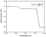
(1) compared with the traditional monochromatic detector, the method realizes that the bias voltage is different from that of the beta-Ga by applying2O3Depletion layers with different depths are formed at the position of the GaN heterojunction, and two working modes of one device are realized, namely the depletion layer is Ga under a small bias voltage (0-5V)2O3A layer, the device being responsive only to light in the solar-blind band below 275 nm; under a larger bias voltage (20-100V), the depletion layer extends to the GaN layer, and the optical response extends to a visible blind band of 365 nm.
(2) An i-type layer is arranged between the n-type layer and the beta-Ga 2O3 layer, so that the absorption of long-wavelength light can be improved under the same bias, and the responsivity and the quantum efficiency of the device can be improved.
(3) The Schottky adopts the transparent electrode, which is beneficial to reducing the absorption of the electrode to light and improving the photocurrent responsivity of the detector.
Detailed Description
The technical solutions in the embodiments of the present invention are clearly and completely described below with reference to the drawings in the embodiments of the present invention, and it is obvious that the described embodiments are only a part of the embodiments of the present invention, and not all of the embodiments. All other embodiments, which can be obtained by a person skilled in the art without any inventive step based on the embodiments of the present invention, are within the scope of the present invention.
Example 1
As shown in FIG. 1, the present beta-Ga2O3The structure of the/GaN heterojunction solar-blind/visible-blind double-color ultraviolet detector sequentially comprises from top to bottom: a substrate layer 1, an n-GaN film layer 2, an i-GaN film layer 3, and beta-Ga2O3Layer 4, and arranged in beta-Ga2O3A p-type electrode 5 on the layer, and an n-type electrode 6 on the n-GaN thin film layer.
Wherein the substrate is a sapphire substrate, the thickness of the n-GaN thin film layer is 1 μm, the thickness of the i-GaN thin film layer is 500nm, and the beta-Ga2O3The thickness of the layer was 300 nm. The p-type electrode is an InGaZnO transparent electrode, and the n-type electrode is a Ti/Al/Ni/Au multilayer electrode.
Fig. 2 and 3 are photocurrent response spectrums of the bichromatic ultraviolet detector of example 1 under different voltages of 0V and 20V. I.e. at a lower bias the depletion layer is Ga2O3A layer, the device being responsive only to light in the solar-blind band below 275 nm; at larger bias, the depletion layer extends to the GaN layer and the optical response extends to the visible blind band of 365 nm.
FIGS. 4 and 5 are graphs of electric field distribution of the dichromatic ultraviolet detector of example 1 under different bias voltages of 0V and 20V, with the depth of depletion layer increasing with the bias voltage, from Ga2O3The layer gradually extends to the GaN layer.
Under the bias voltage of 0-5V, the depletion layer of the device is Ga2O3A layer, the device being responsive only to light in the solar-blind band below 275 nm; under the bias voltage of 20-100V, the depletion layer extends to the GaN layer, and the optical response extends to a visible blind band of 365 nm.
Example 2
beta-Ga of the same formula2O3The structure of the/GaN heterojunction solar-blind/visible-blind double-color ultraviolet detector sequentially comprises from top to bottom: a substrate layer, an n-GaN film layer, an i-GaN film layer, and beta-Ga2O3Layer, and is provided in beta-Ga2O3A p-type electrode on the layer, an n-type electrode disposed on the n-GaN thin film layer.
Wherein the substrate is a Si substrate, the thickness of the n-GaN thin film layer is 10 μm, the thickness of the i-GaN thin film layer is 2000nm, and the beta-Ga2O3The thickness of the layer was 1000 nm. The p-type electrode is a thin-layer Ni/Au transparent electrode, and the n-type electrode is a Ti/Al/Ni/Au multilayer electrode.
Under the bias voltage of 0-20V, the depletion layer of the device is Ga2O3A layer, the device being responsive only to light in the solar-blind band below 275 nm; under the bias voltage of 40-100V, the depletion layer extends to the GaN layer, and the optical response extends to a visible blind band of 365 nm.
Example 3
beta-Ga of the same formula2O3The structure of the/GaN heterojunction solar-blind/visible-blind double-color ultraviolet detector sequentially comprises from top to bottom: a substrate layer, an n-GaN film layer, an i-GaN film layer, and beta-Ga2O3Layer, and is provided in beta-Ga2O3A p-type electrode on the layer, an n-type electrode disposed on the n-GaN thin film layer.
Wherein the substrate is a SiC substrate, the thickness of the n-GaN thin film layer is 5 μm, the thickness of the i-GaN thin film layer is 200nm, and the beta-Ga2O3The thickness of the layer was 200 nm. The p-type electrode is a thin Au transparent electrode, and the n-type electrode is a Ti/Al/Ni/Au multilayer electrode.
Under the bias voltage of 0-2V, the depletion layer of the device is Ga2O3A layer, the device being responsive only to light in the solar-blind band below 275 nm; under the bias voltage of 10-100V, the depletion layer extends to the GaN layer, and the optical response extends to a visible blind band of 365 nm.
Example 4
beta-Ga of the same formula2O3The structure of the/GaN heterojunction solar-blind/visible-blind double-color ultraviolet detector sequentially comprises from top to bottom: a substrate layer, an n-GaN film layer, and beta-Ga2O3Layer, and is provided in beta-Ga2O3A p-type electrode on the layer, an n-type electrode disposed on the n-GaN thin film layer.
Wherein the substrate is a sapphire substrate, the thickness of the n-GaN thin film layer is 1 mu m, and the thickness of the n-GaN thin film layer is beta-Ga2O3The thickness of the layer was 300 nm. The p-type electrode is an InGaZnO transparent electrode, and the n-type electrode is a Ti/Al/Ni/Au multilayer electrode.
Under the bias voltage of 0-5V, the depletion layer of the device is Ga2O3A layer, the device being responsive only to light in the solar-blind band below 275 nm; under the bias voltage of 20-100V, the depletion layer extends to the GaN layer, and the optical response extends to a visible blind band of 365 nm.
Example 5
beta-Ga of the same formula2O3The preparation method of the/GaN heterojunction solar-blind/visible-blind double-color ultraviolet detector comprises the following steps:
1. the sapphire substrate is selected to be subjected to surface high-temperature treatment at 1050 ℃.
2. An n-GaN thin film layer having a thickness of about 1 μm and an i-GaN thin film layer having a thickness of 500nm were prepared on a sapphire substrate by MOCVD at 980 ℃.
3. The temperature is reduced to 600 ℃ by MOCVD, an InN film with the thickness of 10nm is grown to be used as an interface sacrificial layer, and then the InN film is evaporated at the temperature of 700 ℃ by LPCVD.
4. Preparation of 300nm beta-Ga by LPCVD growth in the range of 700-1000 DEG C2O3A thin film layer.
5. Preparing Ti/Al/Ni/Au electrode on n-GaN by etching process, then annealing at 850 deg.C for 30s to form ohmic contact, and then forming ohmic contact on beta-Ga2O3Depositing an InGaZnO transparent electrode on the film to form a Schottky contact, and preparing into beta-Ga2O3a/GaN heterojunction solar-blind/visible-blind double-color ultraviolet detector.
By applying different biases in beta-Ga2O3Depletion layers with different depths are formed at the position of the GaN heterojunction, and two working modes of one device are realized, namely the depletion layer is Ga under smaller bias voltage2O3A layer, the device being responsive only to light in the solar-blind band below 275 nm; at larger bias, the depletion layer extends to the GaN layer and the optical response extends to the visible blind band of 365 nm. In addition, the Schottky adopts an InGaZnO transparent electrode, which is beneficial to reducing the absorption of the electrode to light and improving the photocurrent responsivity of the detector.
The above embodiments are preferred embodiments of the present invention, but the present invention is not limited to the above embodiments, and any other changes, modifications, substitutions, combinations, and simplifications which do not depart from the spirit and principle of the present invention should be construed as equivalents thereof, and all such changes, modifications, substitutions, combinations, and simplifications are intended to be included in the scope of the present invention.