CN111477154B - Communication Architecture of Display Panel and Display Panel - Google Patents
Communication Architecture of Display Panel and Display Panel Download PDFInfo
- Publication number
- CN111477154B CN111477154B CN202010380824.1A CN202010380824A CN111477154B CN 111477154 B CN111477154 B CN 111477154B CN 202010380824 A CN202010380824 A CN 202010380824A CN 111477154 B CN111477154 B CN 111477154B
- Authority
- CN
- China
- Prior art keywords
- memory
- timing controller
- bus switch
- display panel
- communication architecture
- Prior art date
- Legal status (The legal status is an assumption and is not a legal conclusion. Google has not performed a legal analysis and makes no representation as to the accuracy of the status listed.)
- Active
Links
Images

Classifications
-
- G—PHYSICS
- G09—EDUCATION; CRYPTOGRAPHY; DISPLAY; ADVERTISING; SEALS
- G09G—ARRANGEMENTS OR CIRCUITS FOR CONTROL OF INDICATING DEVICES USING STATIC MEANS TO PRESENT VARIABLE INFORMATION
- G09G3/00—Control arrangements or circuits, of interest only in connection with visual indicators other than cathode-ray tubes
- G09G3/20—Control arrangements or circuits, of interest only in connection with visual indicators other than cathode-ray tubes for presentation of an assembly of a number of characters, e.g. a page, by composing the assembly by combination of individual elements arranged in a matrix no fixed position being assigned to or needed to be assigned to the individual characters or partial characters
-
- Y—GENERAL TAGGING OF NEW TECHNOLOGICAL DEVELOPMENTS; GENERAL TAGGING OF CROSS-SECTIONAL TECHNOLOGIES SPANNING OVER SEVERAL SECTIONS OF THE IPC; TECHNICAL SUBJECTS COVERED BY FORMER USPC CROSS-REFERENCE ART COLLECTIONS [XRACs] AND DIGESTS
- Y02—TECHNOLOGIES OR APPLICATIONS FOR MITIGATION OR ADAPTATION AGAINST CLIMATE CHANGE
- Y02D—CLIMATE CHANGE MITIGATION TECHNOLOGIES IN INFORMATION AND COMMUNICATION TECHNOLOGIES [ICT], I.E. INFORMATION AND COMMUNICATION TECHNOLOGIES AIMING AT THE REDUCTION OF THEIR OWN ENERGY USE
- Y02D10/00—Energy efficient computing, e.g. low power processors, power management or thermal management
Landscapes
- Engineering & Computer Science (AREA)
- Physics & Mathematics (AREA)
- Computer Hardware Design (AREA)
- General Physics & Mathematics (AREA)
- Theoretical Computer Science (AREA)
- Control Of Indicators Other Than Cathode Ray Tubes (AREA)
Abstract
一种显示面板的通信架构,通过延时电路的设置,使得写入保护信号可以在流经所述延时电路后延迟对总线开关的开启,直到校验电源管理集成电路中的代码的过程结束,确保时序控制器在进行校验时不会开启所述总线开关,从而避免存储器被校验的通讯内容改写。
A communication structure of a display panel, through the setting of a delay circuit, a write protection signal can delay the opening of a bus switch after flowing through the delay circuit, until the process of verifying codes in a power management integrated circuit ends , to ensure that the sequence controller does not turn on the bus switch when verifying, so as to prevent the memory from being rewritten by the verified communication content.
Description
Technical Field
The invention relates to the technical field of display, in particular to a communication framework and a display panel of a display panel.
Background
After the display panel is powered on, the timing controller typically checks the power management integrated circuit at intervals in order to prevent the code from being overwritten during operation. However, when the timing controller is performing verification, if the verified communication address exactly matches the address of the memory storing the display information (e.g., screen type information), the content of the memory may be rewritten (e.g., screen type information is rewritten), which may cause, for example, the screen type information not to be correctly recognized, resulting in an abnormal picture of the display panel.
Therefore, a communication structure and a display panel of a display panel are needed to solve the technical problems in the prior art.
Disclosure of Invention
The present invention is directed to a communication structure and a display panel of a display panel, so as to solve the problems of the prior art.
In order to achieve the above object, a first aspect of the present invention provides a communication architecture of a display panel, comprising a system on chip electrically connected to a serial bus, a timing controller, a power management integrated circuit, a bus switch, and a memory, the write-in protection terminal on the system on chip is respectively and electrically connected with the time schedule controller, the bus switch and the memory, outputting a write protection signal through the write protection terminal to control the working states of the timing controller, the bus switch, and the memory, the time schedule controller checks codes in the power management integrated circuit through the serial bus at a preset time, the bus switch is arranged between the system on chip and one side of the memory and between the time schedule controller and one side of the power management integrated circuit;
the write protection signal is transmitted to the memory through the phase inverter and is transmitted to the bus switch through the time delay circuit, when the write protection signal with a high level signal is output, the memory is in a readable and writable state, and the write protection signal delays the starting of the bus switch after flowing through the time delay circuit until the process of checking codes in the power management integrated circuit is finished.
Further, the serial bus is an inter-integrated circuit (I) bus 2 C)。
Further, the memory is an Electrically Erasable Programmable Read Only Memory (EEPROM).
Further, the timing controller performs a check during an idle (blanking) time of each frame.
Further, the delay circuit includes a resistor and a capacitor, a first end of the resistor receives the write protect signal, a second end of the resistor is electrically connected to the bus switch and the first end of the capacitor, and the second end of the capacitor is connected to a low level signal compared to the write protect signal.
Further, the bus switch includes a Thin Film Transistor (TFT), and the on and off of the bus switch is implemented by transmitting the write protect signal to a gate terminal of the TFT.
Further, when the write protect signal having a low level signal is output, the timing controller is in a normal operation mode to normally output various control signals for driving the display panel.
Furthermore, the system on chip also outputs a serial signal to the time sequence controller through the serial bus so as to perform display control on the time sequence controller.
Further, the memory stores screen category information, and the system on chip judges the display state of the display panel by reading the screen category information.
A second aspect of the invention provides a display panel comprising the communication architecture of any of the above display panels.
According to the invention, through the arrangement of the delay circuit, the write-in protection signal can delay the starting of the bus switch after flowing through the delay circuit until the process of verifying the code in the power management integrated circuit is finished, so that the bus switch can not be started when the time schedule controller verifies, and the memory is prevented from being rewritten by verified communication contents.
Drawings
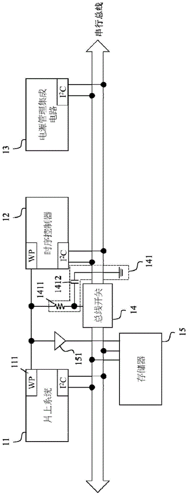
Fig. 1 is a schematic diagram of a communication architecture of a display panel according to an embodiment of the invention.
Detailed Description
In order to make the objects, technical solutions and effects of the present invention clearer and clearer, the present invention is further described in detail below with reference to the accompanying drawings. It should be understood that the specific embodiments described herein are merely illustrative of the invention and are not intended to limit the invention.
The following description of the various embodiments refers to the accompanying drawings, which are included to illustrate embodiments of the invention, and which are set forth in the description and the drawings. The directional terminology used herein is for the purpose of describing particular aspects only and is not intended to be limiting. Accordingly, the directional terms used are used for explanation and understanding of the present invention, and are not used for limiting the present invention.
Referring to fig. 1, fig. 1 is a schematic view of a communication architecture of a display panel according to an embodiment of the invention. The communication architecture includes a system-on-chip (SoC) 11 electrically connected to a serial bus (not shown), a Timing Controller (TCON) 12, a Power Management Integrated Circuit (PMIC) 13, a bus switch 14, and a memory 15, and the bus switch 14 is disposed between the SoC 11 and the memory 15 and between the timing controller 12 and the power management integrated circuit 13. As shown in fig. 1, the system on chip 11 and the memory 15 are disposed on the left side of the bus switch 14, the timing controller 12 and the power management integrated circuit 13 are disposed on the right side of the bus switch 14, and the communication switch between the system on chip 11 side and the timing controller 12 side is controlled by the bus switch 14.
In this embodiment, the serial bus is an inter-integrated circuit (I) bus including a serial data line (SDA) and a Serial Clock Line (SCL) 2 C) The memory 15 is an Electrically Erasable Programmable Read Only Memory (EEPROM). It is understood that the functions and functions of the inter-integrated circuit bus and the eeprom are well known to those skilled in the art and will not be described herein.
In the present embodiment, the system-on-chip 11 outputs a serial signal to the timing controller 12 through the serial bus, so that the timing controller 12 can perform display control such as resolution conversion, image data modulation, and driving frequency conversion. The memory 15 stores screen category information, and the system-on-chip 11 may determine a display state of a display panel by reading the screen category information in the memory 15. In order to explain the present invention more clearly, the memory 15 storing the screen category information will be described below, but this should not be construed as a limitation of the present invention.
In this embodiment, the system on chip 11 is further configured to output a write protection signal (WP) to control the operation states of the timing controller 12, the bus switch 14, and the memory 15, and the WP is simultaneously transmitted to the memory 15 and the bus switch 14 through the inverter 151 and the delay circuit 141, respectively. Specifically, the write protection terminal 111 of the system on chip 11 for outputting the write protection signal is electrically connected to the timing controller 12, the bus switch 14, and the memory 15, respectively. When the timing controller 12 receives the write protect signal with low level, the timing controller 12 is in a normal operation mode (i.e. normally outputs various control signals for driving a display panel), when the bus switch 14 is in an off state, and the memory 15 receives the write protect signal with high level through the inverter 151, so that the write protect signal is in a readable and non-writable state, and when the timing controller 12 receives the write protect signal with high level, the timing controller 12 is in a debug mode (i.e. the system on chip 11 can perform display control on the timing controller 12 through the serial bus), when the bus switch 14 is in an on state, and the memory 15 receives the write protect signal with low level through the inverter 151, making it readable and writable. In one embodiment, the bus switch 14 may include a Thin Film Transistor (TFT) and other electronic components, and the on and off of the bus switch 14 is realized by transmitting the write protection signal to a gate terminal of the TFT.
Further, in order to prevent the code stored in the power management integrated circuit 13 (which may be stored in a non-volatile memory or a flash memory) from being rewritten during the operation of the display panel, the timing controller 12 checks the code in the power management integrated circuit 13 through the serial bus at predetermined time intervals, for example, performs a Cyclic Redundancy Check (CRC) during an idle (blanking) time of each frame.
Since the serial bus is occupied during the verification process, and if the timing controller 12 receives the write protection signal with a high level, the timing controller 12 does not immediately switch to the debug mode, that is, the system on chip 11 cannot immediately control the timing controller 12 through the serial bus, and first waits for the verification process to be completed before switching. However, since the timing controller 12 is not in the debug mode but the write protect signal is a high level signal, the bus switch 14 is turned on and the memory 15 is in a readable and writable state, and if the verified communication address matches the communication address of the memory 15 storing the screen type information, the verified communication content is written into the memory 15, so that the content of the memory 15 (screen type information) is rewritten, and the screen type information cannot be correctly recognized, so that the display image of the display panel is abnormal.
According to the invention, through the arrangement of the delay circuit 141, the write protection signal can delay the starting of the bus switch 14 after flowing through the delay circuit 141 until the process of verifying the code in the power management integrated circuit 13 is finished, so that the bus switch 14 is not started when the timing controller 12 performs verification, and the memory 15 is prevented from being rewritten by verified communication contents. In this way, the soc 11 can read the correct screen type information stored in the memory 15, and correctly identify the screen type or display state, so that the display panel can normally operate to display the correct display image.
Preferably, the delay circuit includes a resistor 1411 and a capacitor 1412, a first end of the resistor 1411 receives the write protection signal, a second end of the resistor 1411 is electrically connected to the bus switch 14 and a first end of the capacitor 1412, and a second end of the capacitor 1412 is connected to a signal with a lower level than the write protection signal (e.g., ground), in which case the delay circuit 141 is a resistor-capacitor delay circuit (RC delay circuit).
The communication architecture of the display panel provided by the present invention can be applied to any type of display panel, such as a liquid crystal display panel (liquid crystal display panel), an organic light-emitting diode display panel (organic light-emitting diode display panel), a quantum display panel (quantum display panel), and the like.
The present invention also provides a display panel, which includes the above communication structure of the display panel, and the communication structure of the display panel is described above and is not repeated.
Although the present invention has been described with reference to the preferred embodiments, it is to be understood that the invention is not limited to the disclosed embodiments, and that various changes and modifications may be effected therein by one skilled in the art without departing from the scope of the invention as defined by the appended claims.
Claims (10)
Priority Applications (1)
| Application Number | Priority Date | Filing Date | Title |
|---|---|---|---|
| CN202010380824.1A CN111477154B (en) | 2020-05-08 | 2020-05-08 | Communication Architecture of Display Panel and Display Panel |
Applications Claiming Priority (1)
| Application Number | Priority Date | Filing Date | Title |
|---|---|---|---|
| CN202010380824.1A CN111477154B (en) | 2020-05-08 | 2020-05-08 | Communication Architecture of Display Panel and Display Panel |
Publications (2)
| Publication Number | Publication Date |
|---|---|
| CN111477154A CN111477154A (en) | 2020-07-31 |
| CN111477154B true CN111477154B (en) | 2022-09-09 |
Family
ID=71762228
Family Applications (1)
| Application Number | Title | Priority Date | Filing Date |
|---|---|---|---|
| CN202010380824.1A Active CN111477154B (en) | 2020-05-08 | 2020-05-08 | Communication Architecture of Display Panel and Display Panel |
Country Status (1)
| Country | Link |
|---|---|
| CN (1) | CN111477154B (en) |
Families Citing this family (2)
| Publication number | Priority date | Publication date | Assignee | Title |
|---|---|---|---|---|
| CN112785957B (en) * | 2021-01-05 | 2023-02-03 | Tcl华星光电技术有限公司 | Driving circuit, display device and control method thereof |
| CN113284452A (en) * | 2021-05-31 | 2021-08-20 | 深圳市华星光电半导体显示技术有限公司 | Display device and control method thereof |
Family Cites Families (5)
| Publication number | Priority date | Publication date | Assignee | Title |
|---|---|---|---|---|
| CN105224425B (en) * | 2015-09-25 | 2018-02-06 | 深圳市共济科技股份有限公司 | The data protection circuit and its method of a kind of storage chip |
| CN208806052U (en) * | 2018-09-30 | 2019-04-30 | 惠科股份有限公司 | display panel drive circuit and display device |
| CN109493894A (en) * | 2018-11-06 | 2019-03-19 | 惠科股份有限公司 | Protection circuit of memory cell in display panel, display panel and display device |
| CN109509422B (en) * | 2018-12-27 | 2021-08-24 | 惠科股份有限公司 | Display panel drive circuit and display device |
| CN109599049B (en) * | 2019-01-28 | 2022-02-08 | 惠科股份有限公司 | Test system and test method for display panel |
-
2020
- 2020-05-08 CN CN202010380824.1A patent/CN111477154B/en active Active
Also Published As
| Publication number | Publication date |
|---|---|
| CN111477154A (en) | 2020-07-31 |
Similar Documents
| Publication | Publication Date | Title |
|---|---|---|
| US11114012B2 (en) | Display panel driving circuit and display device | |
| CN208806052U (en) | display panel drive circuit and display device | |
| WO2021103146A1 (en) | Display panel drive system and display device | |
| JPH05327582A (en) | Program memory rewrite system for portable telephone set | |
| CN111800658B (en) | Chip parameter writing method, television and storage medium | |
| WO2018000471A1 (en) | Data storage device, method for preventing data failure, and time sequence controller | |
| CN110428767B (en) | Driving circuit of display panel and display device | |
| WO2019041396A1 (en) | Method and system for protecting software data in display panel | |
| CN109388345B (en) | Data reading method of memory, display device and computer readable storage medium | |
| CN111477154B (en) | Communication Architecture of Display Panel and Display Panel | |
| US8386694B2 (en) | Memory device, its access method, and memory system | |
| CN109192237B (en) | Memory write protection circuit and display device | |
| CN110767188B (en) | Display panel driving system | |
| US11289040B2 (en) | Driving circuit and driving method of liquid crystal display | |
| US12493420B2 (en) | Configuring data in power management integrated circuit based on circuit board architecture type in a display panel | |
| CN109493894A (en) | Protection circuit of memory cell in display panel, display panel and display device | |
| CN109446851B (en) | Method for protecting data in display panel and display device thereof | |
| CN107291639A (en) | It is a kind of to improve the method and apparatus that bus reads and writes stability | |
| CN116312330A (en) | Display control circuit, control method and electronic equipment | |
| CN104575605A (en) | Memory device and method for booting system using non-volatile memory | |
| JP4083474B2 (en) | MEMORY DEVICE CONTROL METHOD, PROGRAM THEREOF, AND RECORDING MEDIUM | |
| CN116343637B (en) | Driving circuit, driving method and display device | |
| US5224072A (en) | Read-only memory with few programming signal lines | |
| US20250037629A1 (en) | Vehicle display system | |
| WO2020042327A1 (en) | Driving device and driving method |
Legal Events
| Date | Code | Title | Description |
|---|---|---|---|
| PB01 | Publication | ||
| PB01 | Publication | ||
| SE01 | Entry into force of request for substantive examination | ||
| SE01 | Entry into force of request for substantive examination | ||
| GR01 | Patent grant | ||
| GR01 | Patent grant |