CN111448662A - Three-dimensional memory device containing drain select level air gap and method of fabricating the same - Google Patents

Three-dimensional memory device containing drain select level air gap and method of fabricating the same Download PDF

Info

Publication number
CN111448662A
CN111448662A CN201980006271.9A CN201980006271A CN111448662A CN 111448662 A CN111448662 A CN 111448662A CN 201980006271 A CN201980006271 A CN 201980006271A CN 111448662 A CN111448662 A CN 111448662A
Authority
CN
China
Prior art keywords
layer
drain select
dielectric
select level
memory device
Prior art date
Legal status (The legal status is an assumption and is not a legal conclusion. Google has not performed a legal analysis and makes no representation as to the accuracy of the status listed.)
Granted
Application number
CN201980006271.9A
Other languages
Chinese (zh)
Other versions
CN111448662B (en
Inventor
西川昌利
西田彰男
Current Assignee (The listed assignees may be inaccurate. Google has not performed a legal analysis and makes no representation or warranty as to the accuracy of the list.)
SanDisk Technologies LLC
Original Assignee
SanDisk Technologies LLC
Priority date (The priority date is an assumption and is not a legal conclusion. Google has not performed a legal analysis and makes no representation as to the accuracy of the date listed.)
Filing date
Publication date
Application filed by SanDisk Technologies LLC filed Critical SanDisk Technologies LLC
Publication of CN111448662A publication Critical patent/CN111448662A/en
Application granted granted Critical
Publication of CN111448662B publication Critical patent/CN111448662B/en
Active legal-status Critical Current
Anticipated expiration legal-status Critical

Links

Images

Classifications

    • HELECTRICITY
    • H10SEMICONDUCTOR DEVICES; ELECTRIC SOLID-STATE DEVICES NOT OTHERWISE PROVIDED FOR
    • H10BELECTRONIC MEMORY DEVICES
    • H10B41/00Electrically erasable-and-programmable ROM [EEPROM] devices comprising floating gates
    • H10B41/20Electrically erasable-and-programmable ROM [EEPROM] devices comprising floating gates characterised by three-dimensional [3D] arrangements, e.g. with cells on different height levels
    • H10B41/23Electrically erasable-and-programmable ROM [EEPROM] devices comprising floating gates characterised by three-dimensional [3D] arrangements, e.g. with cells on different height levels with source and drain on different levels, e.g. with sloping channels
    • H10B41/27Electrically erasable-and-programmable ROM [EEPROM] devices comprising floating gates characterised by three-dimensional [3D] arrangements, e.g. with cells on different height levels with source and drain on different levels, e.g. with sloping channels the channels comprising vertical portions, e.g. U-shaped channels
    • HELECTRICITY
    • H10SEMICONDUCTOR DEVICES; ELECTRIC SOLID-STATE DEVICES NOT OTHERWISE PROVIDED FOR
    • H10BELECTRONIC MEMORY DEVICES
    • H10B41/00Electrically erasable-and-programmable ROM [EEPROM] devices comprising floating gates
    • H10B41/50Electrically erasable-and-programmable ROM [EEPROM] devices comprising floating gates characterised by the boundary region between the core region and the peripheral circuit region
    • HELECTRICITY
    • H10SEMICONDUCTOR DEVICES; ELECTRIC SOLID-STATE DEVICES NOT OTHERWISE PROVIDED FOR
    • H10BELECTRONIC MEMORY DEVICES
    • H10B43/00EEPROM devices comprising charge-trapping gate insulators
    • H10B43/10EEPROM devices comprising charge-trapping gate insulators characterised by the top-view layout
    • HELECTRICITY
    • H10SEMICONDUCTOR DEVICES; ELECTRIC SOLID-STATE DEVICES NOT OTHERWISE PROVIDED FOR
    • H10BELECTRONIC MEMORY DEVICES
    • H10B43/00EEPROM devices comprising charge-trapping gate insulators
    • H10B43/20EEPROM devices comprising charge-trapping gate insulators characterised by three-dimensional [3D] arrangements, e.g. with cells on different height levels
    • H10B43/23EEPROM devices comprising charge-trapping gate insulators characterised by three-dimensional [3D] arrangements, e.g. with cells on different height levels with source and drain on different levels, e.g. with sloping channels
    • H10B43/27EEPROM devices comprising charge-trapping gate insulators characterised by three-dimensional [3D] arrangements, e.g. with cells on different height levels with source and drain on different levels, e.g. with sloping channels the channels comprising vertical portions, e.g. U-shaped channels
    • HELECTRICITY
    • H10SEMICONDUCTOR DEVICES; ELECTRIC SOLID-STATE DEVICES NOT OTHERWISE PROVIDED FOR
    • H10BELECTRONIC MEMORY DEVICES
    • H10B43/00EEPROM devices comprising charge-trapping gate insulators
    • H10B43/30EEPROM devices comprising charge-trapping gate insulators characterised by the memory core region
    • H10B43/35EEPROM devices comprising charge-trapping gate insulators characterised by the memory core region with cell select transistors, e.g. NAND
    • HELECTRICITY
    • H10SEMICONDUCTOR DEVICES; ELECTRIC SOLID-STATE DEVICES NOT OTHERWISE PROVIDED FOR
    • H10BELECTRONIC MEMORY DEVICES
    • H10B43/00EEPROM devices comprising charge-trapping gate insulators
    • H10B43/40EEPROM devices comprising charge-trapping gate insulators characterised by the peripheral circuit region
    • HELECTRICITY
    • H10SEMICONDUCTOR DEVICES; ELECTRIC SOLID-STATE DEVICES NOT OTHERWISE PROVIDED FOR
    • H10BELECTRONIC MEMORY DEVICES
    • H10B43/00EEPROM devices comprising charge-trapping gate insulators
    • H10B43/50EEPROM devices comprising charge-trapping gate insulators characterised by the boundary region between the core and peripheral circuit regions
    • HELECTRICITY
    • H10SEMICONDUCTOR DEVICES; ELECTRIC SOLID-STATE DEVICES NOT OTHERWISE PROVIDED FOR
    • H10DINORGANIC ELECTRIC SEMICONDUCTOR DEVICES
    • H10D30/00Field-effect transistors [FET]
    • H10D30/60Insulated-gate field-effect transistors [IGFET]
    • H10D30/69IGFETs having charge trapping gate insulators, e.g. MNOS transistors
    • H10D30/694IGFETs having charge trapping gate insulators, e.g. MNOS transistors characterised by the shapes, relative sizes or dispositions of the gate electrodes
    • HELECTRICITY
    • H10SEMICONDUCTOR DEVICES; ELECTRIC SOLID-STATE DEVICES NOT OTHERWISE PROVIDED FOR
    • H10DINORGANIC ELECTRIC SEMICONDUCTOR DEVICES
    • H10D62/00Semiconductor bodies, or regions thereof, of devices having potential barriers
    • H10D62/10Shapes, relative sizes or dispositions of the regions of the semiconductor bodies; Shapes of the semiconductor bodies
    • H10D62/113Isolations within a component, i.e. internal isolations
    • H10D62/115Dielectric isolations, e.g. air gaps
    • HELECTRICITY
    • H10SEMICONDUCTOR DEVICES; ELECTRIC SOLID-STATE DEVICES NOT OTHERWISE PROVIDED FOR
    • H10WGENERIC PACKAGES, INTERCONNECTIONS, CONNECTORS OR OTHER CONSTRUCTIONAL DETAILS OF DEVICES COVERED BY CLASS H10
    • H10W20/00Interconnections in chips, wafers or substrates
    • H10W20/01Manufacture or treatment
    • H10W20/071Manufacture or treatment of dielectric parts thereof
    • H10W20/074Manufacture or treatment of dielectric parts thereof of dielectric parts comprising thin functional dielectric layers, e.g. dielectric etch-stop, barrier, capping or liner layers
    • HELECTRICITY
    • H10SEMICONDUCTOR DEVICES; ELECTRIC SOLID-STATE DEVICES NOT OTHERWISE PROVIDED FOR
    • H10BELECTRONIC MEMORY DEVICES
    • H10B41/00Electrically erasable-and-programmable ROM [EEPROM] devices comprising floating gates
    • H10B41/10Electrically erasable-and-programmable ROM [EEPROM] devices comprising floating gates characterised by the top-view layout
    • HELECTRICITY
    • H10SEMICONDUCTOR DEVICES; ELECTRIC SOLID-STATE DEVICES NOT OTHERWISE PROVIDED FOR
    • H10BELECTRONIC MEMORY DEVICES
    • H10B41/00Electrically erasable-and-programmable ROM [EEPROM] devices comprising floating gates
    • H10B41/30Electrically erasable-and-programmable ROM [EEPROM] devices comprising floating gates characterised by the memory core region
    • H10B41/35Electrically erasable-and-programmable ROM [EEPROM] devices comprising floating gates characterised by the memory core region with a cell select transistor, e.g. NAND
    • HELECTRICITY
    • H10SEMICONDUCTOR DEVICES; ELECTRIC SOLID-STATE DEVICES NOT OTHERWISE PROVIDED FOR
    • H10BELECTRONIC MEMORY DEVICES
    • H10B41/00Electrically erasable-and-programmable ROM [EEPROM] devices comprising floating gates
    • H10B41/40Electrically erasable-and-programmable ROM [EEPROM] devices comprising floating gates characterised by the peripheral circuit region

Landscapes

  • Semiconductor Memories (AREA)
  • Non-Volatile Memory (AREA)

Abstract

A three-dimensional memory device comprising: an alternating stack of insulating layers and word lines over a substrate; a memory stack structure extending through the alternating stack and containing respective vertical semiconductor channels and respective memory films; a drain select gate electrode over the alternating stack extending along a first horizontal direction and laterally spaced along a second horizontal direction; and a dielectric cap layer between adjacent drain select gate electrodes. An air gap is located in the dielectric cap layer between adjacent drain select gate electrodes.

Description

含有漏极选择层级气隙的三维存储器装置及其制造方法Three-dimensional memory device with drain selective level air gap and method of making the same

相关申请案related applications

本申请案要求2018年8月20日提交的第62/719,893号美国临时专利申请和2018年9月20日提交的第16/136,686号美国非临时专利申请案的权益,以上申请的全部内容以引用的方式并入本文中。This application claims the benefit of US Provisional Patent Application No. 62/719,893, filed August 20, 2018, and US Non-Provisional Patent Application No. 16/136,686, filed September 20, 2018, the entire contents of which Incorporated herein by reference.

技术领域technical field

本公开大体上涉及半导体装置的领域,且特别涉及含有漏极选择层级气隙的三维存储器装置及其制造方法。The present disclosure relates generally to the field of semiconductor devices, and in particular, to three-dimensional memory devices including drain selective level air gaps and methods of fabricating the same.

背景技术Background technique

在T.Endoh等的标题为“具有堆叠包围栅极晶体管(S-SGT)结构化单元的新型超高密度存储器(Novel Ultra High Density Memory With A Stacked-Surrounding GateTransistor(S-SGT)Structured Cell)”(IEDM学报(2001)33-36)的论文中公开了每单元具有一个位的三维竖直NAND串。Titled "Novel Ultra High Density Memory With A Stacked-Surrounding Gate Transistor (S-SGT) Structured Cell" by T. Endoh et al. A three-dimensional vertical NAND string with one bit per cell is disclosed in a paper in (IEDM Journal (2001) 33-36).

发明内容SUMMARY OF THE INVENTION

根据本公开的方面,一种三维存储器装置包含位于衬底上方的绝缘层和字线的交替堆叠,延伸穿过所述交替堆叠且含有相应竖直半导体通道和相应存储器膜的存储器堆叠结构,位于交替堆叠上方、沿着第一水平方向延伸且沿着第二水平方向横向隔开的漏极选择栅极电极,以及位于邻近漏极选择栅极电极之间的电介质顶盖层。气隙在邻近漏极选择栅极电极之间位于所述电介质顶盖层中。According to an aspect of the present disclosure, a three-dimensional memory device includes alternating stacks of insulating layers and word lines over a substrate, a memory stack structure extending through the alternating stack and containing respective vertical semiconductor channels and respective memory films, located at Overlying drain select gate electrodes extending along a first horizontal direction and laterally spaced along a second horizontal direction are alternately stacked, and a dielectric cap layer between adjacent drain select gate electrodes. An air gap is located in the dielectric cap layer between adjacent drain select gate electrodes.

根据本公开的另一方面,提供一种形成三维存储器装置的方法,其包括:在衬底上方形成绝缘层和间隔物材料层的交替堆叠,其中间隔物材料层被形成为字线层级导电层或被字线层级导电层代替;形成穿过交替堆叠的存储器堆叠结构,其中存储器堆叠结构中的每一个包括相应竖直半导体通道和相应存储器膜;在交替堆叠上方形成模板轨道结构;在存储器堆叠结构上方形成漏极选择层级柱结构,其中漏极选择层级柱结构中的每一个包括接触存储器堆叠结构中的下伏存储器堆叠结构的漏极选择层级通道;在交替堆叠上方和相邻对的模板轨道结构之间形成漏极选择层级电极条带;通过移除模板轨道结构形成横向延伸沟槽;以及在横向延伸沟槽中和漏极选择层级电极条带上方形成电介质顶盖层,其中电介质顶盖层包括上覆于漏极选择层级电极条带的平坦部分和填充横向延伸沟槽且位于相邻对的漏极选择层级电极条带之间的向下突出轨道部分,其中向下突出轨道部分中的每一个包括不含任何固相材料或任何液相材料的腔。According to another aspect of the present disclosure, there is provided a method of forming a three-dimensional memory device comprising forming an alternating stack of insulating layers and spacer material layers over a substrate, wherein the spacer material layers are formed as word line level conductive layers or replaced by word line level conductive layers; forming memory stacks through alternating stacks, wherein each of the memory stacks includes respective vertical semiconductor channels and respective memory films; forming template track structures over the alternating stacks; over the memory stacks forming a drain select level pillar structure over the structure, wherein each of the drain select level pillar structures includes a drain select level channel contacting an underlying memory stack structure in the memory stack structure; over the alternating stack and adjacent pairs of templates forming drain select level electrode strips between the track structures; forming laterally extending trenches by removing the template track structures; and forming a dielectric cap layer in the laterally extending trenches and over the drain select level electrode strips, wherein the dielectric top The capping layer includes a flat portion overlying the drain select level electrode strips and a downwardly projecting track portion filling the laterally extending trench and between adjacent pairs of the drain select level electrode strips, wherein the downwardly projecting track portion Each of these includes a cavity that does not contain any solid phase material or any liquid phase material.

附图说明Description of drawings

图1A是根据本公开的第一实施例的在形成至少一个外围装置和处理中源极层级材料层之后的示例性结构的竖直横截面图。1A is a vertical cross-sectional view of an exemplary structure after forming at least one peripheral device and an in-process source level material layer according to a first embodiment of the present disclosure.

图1B是图1A的处理中源极层级材料层的放大图。FIG. 1B is an enlarged view of the in-process source level material layer of FIG. 1A .

图2是根据本公开的实施例的在形成绝缘层和牺牲材料层的交替堆叠之后的示例性结构的竖直横截面图。2 is a vertical cross-sectional view of an exemplary structure after forming alternating stacks of insulating layers and sacrificial material layers in accordance with an embodiment of the present disclosure.

图3是根据本公开的实施例的在形成阶梯式阶台和逆向阶梯式电介质材料部分之后的示例性结构的竖直横截面图。3 is a vertical cross-sectional view of an exemplary structure after forming stepped steps and reverse stepped dielectric material portions in accordance with an embodiment of the present disclosure.

图4A是根据本公开的实施例的在形成存储器开口之后的示例性结构的竖直横截面图。4A is a vertical cross-sectional view of an exemplary structure after forming a memory opening in accordance with an embodiment of the present disclosure.

图4B是图4A的示例性结构的俯视图。铰接竖直平面A-A'是图4A的竖直横截面图的平面。4B is a top view of the exemplary structure of FIG. 4A. The hinged vertical plane AA' is the plane of the vertical cross-sectional view of Figure 4A.

图5A-5D是根据本公开的实施例的在存储器开口填充结构的形成期间的存储器开口的竖直横截面图。5A-5D are vertical cross-sectional views of memory openings during formation of a memory opening fill structure in accordance with embodiments of the present disclosure.

图6A是根据本公开的实施例的在形成存储器堆叠结构之后的示例性结构的竖直横截面图。6A is a vertical cross-sectional view of an exemplary structure after forming a memory stack structure in accordance with an embodiment of the present disclosure.

图6B是图6A的示例性结构的俯视图。铰接竖直平面A-A'是图6A的竖直横截面图的平面。6B is a top view of the exemplary structure of FIG. 6A. The hinged vertical plane AA' is the plane of the vertical cross-sectional view of Figure 6A.

图6C是沿着图6B中的竖直平面C-C'的示例性结构的区的竖直横截面图。Figure 6C is a vertical cross-sectional view of a region of the exemplary structure along vertical plane CC' in Figure 6B.

图7A是根据本公开的实施例的在形成电介质蚀刻终止层和牺牲填充材料层之后的示例性结构的竖直横截面图。7A is a vertical cross-sectional view of an exemplary structure after forming a dielectric etch stop layer and a sacrificial fill material layer in accordance with an embodiment of the present disclosure.

图7B是图7A的示例性结构的区的竖直横截面图。7B is a vertical cross-sectional view of a region of the exemplary structure of FIG. 7A.

图8是根据本公开的实施例的在形成沟槽之后的示例性结构的区的竖直横截面图。8 is a vertical cross-sectional view of a region of an exemplary structure after trenches are formed in accordance with an embodiment of the present disclosure.

图9是根据本公开的实施例的在形成牺牲衬里之后的示例性结构的竖直横截面图。9 is a vertical cross-sectional view of an exemplary structure after formation of a sacrificial liner in accordance with an embodiment of the present disclosure.

图10A是根据本公开的实施例的在形成模板轨道结构之后的示例性结构的竖直横截面图。10A is a vertical cross-sectional view of an exemplary structure after forming a template track structure in accordance with an embodiment of the present disclosure.

图10B是图10A的示例性结构的俯视图。竖直平面A-A'是图10A的竖直横截面图的平面。10B is a top view of the exemplary structure of FIG. 10A. Vertical plane AA' is the plane of the vertical cross-sectional view of Figure 10A.

图11是根据本公开的实施例的在形成电介质顶盖之后的示例性结构的竖直横截面图。11 is a vertical cross-sectional view of an exemplary structure after forming a dielectric cap in accordance with an embodiment of the present disclosure.

图12A是根据本公开的实施例的在形成漏极选择层级开口之后的示例性结构的竖直横截面图。12A is a vertical cross-sectional view of an exemplary structure after forming a drain select level opening in accordance with an embodiment of the present disclosure.

图12B是图12A的示例性结构的俯视图。竖直平面A-A'是图12A的竖直横截面图的平面。12B is a top view of the exemplary structure of FIG. 12A. Vertical plane AA' is the plane of the vertical cross-sectional view of Figure 12A.

图13A是根据本公开的实施例的在形成圆柱形电介质间隔物之后的示例性结构的竖直横截面图。13A is a vertical cross-sectional view of an exemplary structure after formation of cylindrical dielectric spacers in accordance with an embodiment of the present disclosure.

图13B是图13A的示例性结构的俯视图。竖直平面A-A'是图13A的竖直横截面图的平面。13B is a top view of the exemplary structure of FIG. 13A. Vertical plane AA' is the plane of the vertical cross-sectional view of Figure 13A.

图14是根据本公开的实施例的在形成栅极电极层之后的示例性结构的竖直横截面图。14 is a vertical cross-sectional view of an exemplary structure after forming a gate electrode layer according to an embodiment of the present disclosure.

图15是根据本公开的实施例的在形成圆柱形栅极电极之后的示例性结构的竖直横截面图。15 is a vertical cross-sectional view of an exemplary structure after forming a cylindrical gate electrode according to an embodiment of the present disclosure.

图16是根据本公开的实施例的在形成栅极电介质层和覆盖材料层之后的示例性结构的竖直横截面图。16 is a vertical cross-sectional view of an exemplary structure after forming a gate dielectric layer and a capping material layer in accordance with an embodiment of the present disclosure.

图17是根据本公开的实施例的在形成栅极电介质和覆盖材料间隔物之后的示例性结构的竖直横截面图。17 is a vertical cross-sectional view of an exemplary structure after forming gate dielectric and capping material spacers in accordance with an embodiment of the present disclosure.

图18是根据本公开的实施例的在形成漏极选择层级半导体通道层和漏极层级电介质芯层之后的示例性结构的竖直横截面图。18 is a vertical cross-sectional view of an exemplary structure after forming a drain select level semiconductor channel layer and a drain level dielectric core layer in accordance with an embodiment of the present disclosure.

图19是根据本公开的实施例的在形成漏极层级电介质芯之后的示例性结构的竖直横截面图。19 is a vertical cross-sectional view of an exemplary structure after forming a drain-level dielectric core in accordance with an embodiment of the present disclosure.

图20是根据本公开的实施例的在形成漏极层级层级通道之后的示例性结构的竖直横截面图。20 is a vertical cross-sectional view of an exemplary structure after forming a drain level level channel according to an embodiment of the present disclosure.

图21是根据本公开的实施例的在形成电介质漏极间隔物之后的示例性结构的竖直横截面图。21 is a vertical cross-sectional view of an exemplary structure after forming a dielectric drain spacer in accordance with an embodiment of the present disclosure.

图22A是根据本公开的实施例的在形成漏极区之后的示例性结构的竖直横截面图。22A is a vertical cross-sectional view of an exemplary structure after forming a drain region in accordance with an embodiment of the present disclosure.

图22B是图22A的示例性结构的俯视图。竖直平面A-A'是图22A的竖直横截面图的平面。Figure 22B is a top view of the exemplary structure of Figure 22A. Vertical plane AA' is the plane of the vertical cross-sectional view of Figure 22A.

图22C是沿着平面C-C'的示例性结构的竖直横截面图。22C is a vertical cross-sectional view of an exemplary structure along plane CC'.

图23A-23H是根据本公开的实施例的在用源极层级材料层代替处理中源极层级材料层期间的示例性结构的区的顺序竖直横截面图。23A-23H are sequential vertical cross-sectional views of regions of an exemplary structure during replacement of a source level material layer in processing with a source level material layer in accordance with embodiments of the present disclosure.

图24是根据本公开的实施例的在背侧沟槽中形成电介质壁结构之后的示例性结构的竖直横截面图。24 is a vertical cross-sectional view of an exemplary structure after forming a dielectric wall structure in a backside trench in accordance with an embodiment of the present disclosure.

图25是根据本公开的实施例的在移除牺牲覆盖层之后的示例性结构的竖直横截面图。25 is a vertical cross-sectional view of an exemplary structure after removal of the sacrificial capping layer in accordance with an embodiment of the present disclosure.

图26到30是根据本公开的实施例的用于形成漏极选择层级栅极电极的步骤的竖直横截面图。26 to 30 are vertical cross-sectional views of steps for forming a drain select level gate electrode according to embodiments of the present disclosure.

图31A是根据本公开的实施例的在形成气隙之后的示例性结构的竖直横截面图。31A is a vertical cross-sectional view of an exemplary structure after forming an air gap, according to an embodiment of the present disclosure.

图31B是图31A的示例性结构的俯视图。竖直平面A-A'是图31A的竖直横截面图的平面。31B is a top view of the exemplary structure of FIG. 31A. Vertical plane AA' is the plane of the vertical cross-sectional view of Figure 31A.

图31C是沿着铰接竖直平面C-C'的图31B的示例性结构的竖直横截面图。31C is a vertical cross-sectional view of the exemplary structure of FIG. 31B along hinged vertical plane CC'.

具体实施方式Detailed ways

漏极选择晶体管用以选择性地激活存储器串而不激活相邻存储器串。漏极选择晶体管位于漏极选择层级中且包含漏极层级选择栅极电极。沿着长度方向延伸的漏极选择层级隔离结构用以提供邻近漏极选择晶体管之间的电隔离。随着漏极选择晶体管的尺寸收缩,漏极选择层级隔离结构的宽度也减小。因此,漏极选择层级隔离结构变得容易发生电介质击穿,且漏极选择晶体管的漏极层级选择栅极电极的相邻对之间的电容性耦合增加。本公开的实施例是针对含有漏极选择层级气隙(在本文中也被称为“腔隔离”)的三维存储器装置及减小上述电介质击穿和电容性耦合的其制造方法。本公开的实施例可用以形成包含多层级存储器结构的各种结构,本公开的非限制性实例包含包括多个NAND存储器串的半导体装置,例如三维单片存储器阵列装置。Drain select transistors are used to selectively activate memory strings without activating adjacent memory strings. A drain select transistor is located in the drain select level and includes a drain level select gate electrode. A drain select level isolation structure extending along the length is used to provide electrical isolation between adjacent drain select transistors. As the size of the drain select transistor shrinks, the width of the drain select level isolation structure also decreases. Therefore, the drain selection level isolation structure becomes prone to dielectric breakdown and the capacitive coupling between adjacent pairs of drain level selection gate electrodes of the drain selection transistor increases. Embodiments of the present disclosure are directed to three-dimensional memory devices containing a drain-selective level air gap (also referred to herein as "cavity isolation") and methods of making the same that reduce the aforementioned dielectric breakdown and capacitive coupling. Embodiments of the present disclosure may be used to form various structures including multi-level memory structures, non-limiting examples of the present disclosure including semiconductor devices including multiple NAND memory strings, such as three-dimensional monolithic memory array devices.

图式未按比例绘制。除非明确地描述或以其它方式清楚地指示不存在元件的重复,否则在说明元件的单个个例的情况下,可重复元件的多个个例。例如“第一”、“第二”以及“第三”的序数仅用以识别类似元件,且可跨越本公开的说明书和权利要求书采用不同序数。相同附图标记指代相同元件或类似元件。除非另外指示,否则假定具有相同附图标号的元件具有相同组成。除非另外指示,否则元件之间的“接触”指代元件之间的直接接触,其提供由所述元件共享的边缘或表面。如本文中所使用,位于第二元件“上”的第一元件可以位于第二元件的表面的外侧上或第二元件的内侧上。如本文中所使用,如果第一元件的表面与第二元件的表面之间存在物理接触,那么第一元件“直接”位于第二元件“上”。Figures are not drawn to scale. Where a single instance of an element is illustrated, multiple instances of an element may be repeated unless explicitly described or otherwise clearly indicated that there is no repetition of the element. Ordinals such as "first," "second," and "third" are used only to identify similar elements, and different ordinal numbers may be employed across the description and claims of the present disclosure. The same reference numbers refer to the same or similar elements. Elements with the same reference numerals are assumed to have the same composition unless otherwise indicated. Unless otherwise indicated, "contact" between elements refers to direct contact between the elements that provides an edge or surface shared by the elements. As used herein, a first element "on" a second element can be on the outside of the surface of the second element or on the inside of the second element. As used herein, a first element is "directly on" a second element if there is physical contact between the surface of the first element and the surface of the second element.

如本文中所使用,“层”指代包含具有厚度的区的材料部分。层可以在整个下伏或上覆结构上方延伸,或可具有小于下伏或上覆结构的范围的范围。另外,层可以是厚度小于连续结构的厚度的均质或非均质连续结构的区域。举例来说,层可定位于在连续结构的顶部表面与底部表面之间或在连续结构的顶部表面和底部表面处的任何对水平平面之间。层可水平地、竖直地和/或沿着锥形表面延伸。衬底可以是层,所述层可包含其中的一或多个层,或可具有其上、其上方和/或其下的一或多个层。As used herein, a "layer" refers to a portion of a material comprising a region of thickness. A layer may extend over the entire underlying or overlying structure, or may have an extent less than that of the underlying or overlying structure. Additionally, a layer may be a region of a homogeneous or heterogeneous continuous structure having a thickness less than the thickness of the continuous structure. For example, a layer may be positioned between the top and bottom surfaces of the continuous structure or between any pair of horizontal planes at the top and bottom surfaces of the continuous structure. The layers may extend horizontally, vertically and/or along a tapered surface. A substrate may be a layer, which may include one or more layers therein, or may have one or more layers thereon, over it, and/or under it.

单片三维存储器阵列是其中在如半导体晶片的单个衬底上方形成多个存储器级而不具有中间衬底的存储器阵列。术语“单片”意味着阵列的每一层级的层直接沉积于阵列的每一下伏层级的层上。相比之下,二维阵列可单独形成,且接着封装在一起以形成非单片存储器装置。例如,非单片堆叠存储器已通过在单独衬底上形成存储器层级且竖直地堆叠所述存储器层级来构建,如标题为“三维结构存储器(Three-dimensional StructureMemory)”的第5,915,167号美国专利中所描述。衬底可在接合之前薄化或从存储器层级去除,但由于存储器层级起初形成于单独衬底上方,因此此类存储器不是真正单片三维存储器阵列。本公开的各种三维存储器装置包含单片三维NAND串存储器装置,且可采用本文中所描述的各种实施例来制造。Monolithic three-dimensional memory arrays are memory arrays in which multiple memory levels are formed over a single substrate, such as a semiconductor wafer, without an intervening substrate. The term "monolithic" means that the layers of each level of the array are deposited directly on the layers of each underlying level of the array. In contrast, two-dimensional arrays can be formed individually and then packaged together to form non-monolithic memory devices. For example, non-monolithic stacked memories have been constructed by forming memory levels on separate substrates and stacking the memory levels vertically, as in US Pat. No. 5,915,167 entitled "Three-dimensional Structure Memory" Described. The substrates can be thinned or removed from the memory levels prior to bonding, but since the memory levels are initially formed over separate substrates, such memories are not true monolithic three-dimensional memory arrays. Various three-dimensional memory devices of the present disclosure include monolithic three-dimensional NAND string memory devices, and may be fabricated using the various embodiments described herein.

参考图1A和1B,示出根据本公开的实施例的示例性结构,其可用于例如制造含有竖直NAND存储器装置的装置结构。示例性结构包含衬底8,例如硅晶片或绝缘体硅片衬底。衬底8可包含在其上部部分中的衬底半导体层9。衬底半导体层9可以是硅晶片8的上部部分、硅晶片8的上部部分中的掺杂阱,或位于衬底的顶部表面上方的半导体(例如,硅)层。衬底8可具有主表面7,其可为例如衬底半导体层9的最顶部表面。主表面7可为半导体表面。在一个实施例中,主表面7可为单晶半导体表面,例如单晶硅表面。Referring to FIGS. 1A and 1B , exemplary structures according to embodiments of the present disclosure are shown, which may be used, for example, to fabricate device structures including vertical NAND memory devices. Exemplary structures include a substrate 8, such as a silicon wafer or a silicon-on-insulator substrate. The substrate 8 may include a substrate semiconductor layer 9 in an upper portion thereof. The substrate semiconductor layer 9 may be an upper portion of the silicon wafer 8, a doped well in the upper portion of the silicon wafer 8, or a semiconductor (eg, silicon) layer over the top surface of the substrate. The substrate 8 may have a major surface 7 , which may be, for example, the topmost surface of the substrate semiconductor layer 9 . The main surface 7 may be a semiconductor surface. In one embodiment, the main surface 7 may be a single crystal semiconductor surface, such as a single crystal silicon surface.

如本文中所使用,“半导性材料”是指具有1.0×10-6S/cm到1.0×105S/cm的范围内的电导率的材料。如本文中所使用,“半导体材料”指代在其中不存在电掺杂剂的情况下,具有从1.0×10-6S/cm到1.0×105S/cm的范围内的电导率的材料,且其能够在与电掺杂剂的合适掺杂后产生具有从1.0S/cm到1.0×105S/cm的范围内的电导率的掺杂材料。如本文中所使用,“电掺杂剂”指代将空穴添加到能带结构内的价带的p型掺杂剂,或将电子添加到能带结构内的导带的n型掺杂剂。如本文中所使用,“导电材料”指代具有大于1.0×105S/cm的电导率的材料。如本文中所使用,“绝缘体材料”或“电介质材料”指代具有小于1.0×10-6S/cm的电导率的材料。如本文所使用,“重掺杂半导体材料”指代以充分高原子浓度掺杂有电掺杂剂以变为导电材料的半导体材料,其形成为结晶材料或通过退火过程(例如,从初始非晶态)转换为结晶材料,即,具有大于1.0×105S/cm的电导率。“掺杂半导体材料”可为重掺杂半导体材料,或可为包含提供从1.0×10-6S/cm到1.0×105S/cm的范围内的电导率的浓度下的电掺杂剂(即,p型掺杂剂和/或n型掺杂剂)的半导体材料。“本征半导体材料”指代并不掺杂有电掺杂剂的半导体材料。因此,半导体材料可为半导性或传导性的,且可为本征半导体材料或掺杂半导体材料。掺杂半导体材料可取决于其中的电掺杂剂的原子浓度而是半导性或传导性的。如本文中所使用,“金属材料”是指其中包含至少一种金属元素的导电材料。针对电导率的所有测量均在标准条件下进行。As used herein, "semiconductive material" refers to a material having an electrical conductivity in the range of 1.0×10 −6 S/cm to 1.0×10 5 S/cm. As used herein, "semiconductor material" refers to a material having an electrical conductivity in the range from 1.0x10⁻⁶ S/cm to 1.0x10⁵ S/cm in the absence of electrical dopants in it , and it is capable of producing doped materials with conductivities ranging from 1.0 S/cm to 1.0×10 5 S/cm after suitable doping with electrical dopants. As used herein, "electrical dopant" refers to a p-type dopant that adds holes to the valence band within the band structure, or an n-type dopant that adds electrons to the conduction band within the band structure agent. As used herein, "conductive material" refers to a material having an electrical conductivity greater than 1.0×10 5 S/cm. As used herein, "insulator material" or "dielectric material" refers to a material having an electrical conductivity of less than 1.0 x 10⁻⁶ S/cm. As used herein, "heavily doped semiconductor material" refers to a semiconductor material that is doped with an electrical dopant at a sufficiently high atomic concentration to become a conductive material, either formed as a crystalline material or by an annealing process (eg, from an initial non- crystalline state) into a crystalline material, ie, having a conductivity greater than 1.0×10 5 S/cm. A "doped semiconductor material" may be a heavily doped semiconductor material, or may include an electrical dopant at a concentration that provides an electrical conductivity in the range from 1.0 x 10⁻⁶ S/cm to 1.0 x 10⁵ S/cm (ie, p-type dopants and/or n-type dopants). "Intrinsic semiconductor material" refers to a semiconductor material that is not doped with electrical dopants. Thus, the semiconductor material may be semiconducting or conductive, and may be an intrinsic semiconductor material or a doped semiconductor material. A doped semiconductor material can be semiconducting or conductive depending on the atomic concentration of the electrical dopants therein. As used herein, "metallic material" refers to a conductive material containing at least one metal element therein. All measurements for conductivity were performed under standard conditions.

用于外围电路的至少一个半导体装置700可形成于衬底半导体层9的一部分上。所述至少一个半导体装置可包含例如场效应晶体管。举例来说,至少一个浅沟槽隔离结构720可通过蚀刻衬底半导体层9的部分且在其中沉积电介质材料而形成。栅极电介质层、至少一个栅极导体层和栅极顶盖电介质层可形成于衬底半导体层9上方,且可随后图案化以形成至少一个栅极结构(750、752、754、758),所述栅极结构中的每一个可包含栅极电介质750、栅极电极(752、754)和栅极顶盖电介质758。栅极电极(752、754)可包含第一栅极电极部分752和第二栅电极部分754的堆叠。至少一个栅极间隔物756可通过沉积和各向异性地蚀刻电介质衬里而形成在所述至少一个栅极结构(750、752、754、758)周围。有源区730可例如通过采用至少一个栅极结构(750、752、754、758)作为掩模结构来引入电掺杂剂而形成于衬底半导体层9的上部部分中。额外掩模可视需要而采用。有源区730可包含场效应晶体管的源极区和漏极区。可任选地形成第一电介质衬里761和第二电介质衬里762。第一和第二电介质衬里(761、762)中的每一个可包括氧化硅层、氮化硅层和/或电介质金属氧化物层。如本文中所使用,氧化硅包含二氧化硅以及每一硅原子具有大于或小于两个氧原子的非化学计量氧化硅。二氧化硅是优选的。在说明性实例中,第一电介质衬里761可以是氧化硅层,且第二电介质衬里762可以是氮化硅层。用于外围电路的至少一个半导体装置可含有用于待随后形成的存储器装置的驱动器电路,所述存储器装置可包含至少一个NAND装置。如氧化硅的电介质材料可沉积在至少一个半导体装置上方,且可随后平坦化以形成平坦化电介质层770。包含至少一个半导体装置700的区在本文中被称为外围装置区200。At least one semiconductor device 700 for peripheral circuits may be formed on a portion of the substrate semiconductor layer 9 . The at least one semiconductor device may comprise, for example, a field effect transistor. For example, at least one shallow trench isolation structure 720 may be formed by etching portions of substrate semiconductor layer 9 and depositing a dielectric material therein. A gate dielectric layer, at least one gate conductor layer, and a gate capping dielectric layer can be formed over the substrate semiconductor layer 9, and can then be patterned to form at least one gate structure (750, 752, 754, 758), so Each of the gate structures may include a gate dielectric 750 , gate electrodes ( 752 , 754 ) and a gate capping dielectric 758 . The gate electrodes ( 752 , 754 ) may comprise a stack of a first gate electrode portion 752 and a second gate electrode portion 754 . At least one gate spacer 756 may be formed around the at least one gate structure (750, 752, 754, 758) by depositing and anisotropically etching a dielectric liner. The active region 730 may be formed in the upper portion of the substrate semiconductor layer 9, eg, by introducing electrical dopants using at least one gate structure (750, 752, 754, 758) as a mask structure. Additional masks may be used as needed. The active region 730 may include source and drain regions of a field effect transistor. A first dielectric liner 761 and a second dielectric liner 762 can optionally be formed. Each of the first and second dielectric liners (761, 762) may include a silicon oxide layer, a silicon nitride layer, and/or a dielectric metal oxide layer. As used herein, silicon oxide includes silicon dioxide as well as non-stoichiometric silicon oxides having more or less than two oxygen atoms per silicon atom. Silica is preferred. In an illustrative example, first dielectric liner 761 may be a silicon oxide layer, and second dielectric liner 762 may be a silicon nitride layer. At least one semiconductor device for peripheral circuits may contain driver circuits for memory devices to be subsequently formed, which may include at least one NAND device. A dielectric material, such as silicon oxide, can be deposited over the at least one semiconductor device, and can then be planarized to form planarized dielectric layer 770 . The region containing at least one semiconductor device 700 is referred to herein as peripheral device region 200 .

电介质材料层768可形成于衬底半导体层9上方。电介质材料层768可包含单个电介质材料层或多个电介质材料层。电介质材料层768可包含掺杂硅酸盐玻璃、未掺杂硅酸盐玻璃和有机硅酸盐玻璃中的任一种或多种。在一个实施例中,所述至少一个电介质材料层768可包括具有不超过未掺杂硅酸盐玻璃(即,氧化硅)的3.9的介电常数的介电常数的电介质材料层或基本上由所述电介质材料层组成。A layer of dielectric material 768 may be formed over the substrate semiconductor layer 9 . Dielectric material layer 768 may comprise a single dielectric material layer or multiple dielectric material layers. The layer of dielectric material 768 may comprise any one or more of doped silicate glass, undoped silicate glass, and organosilicate glass. In one embodiment, the at least one layer of dielectric material 768 may comprise a layer of dielectric material having a dielectric constant that does not exceed the dielectric constant of undoped silicate glass (ie, silicon oxide) of 3.9 or consists essentially of The dielectric material layer is composed.

可将任选金属材料层和半导体材料层沉积在电介质材料层768上方或沉积于电介质材料层的图案化凹部内,且进行光刻图案化以提供任选导电板层6和处理中源极层级材料层10'。如本文所使用,“处理中”元件指代在后续处理步骤期间被修改的元件。任选的导电板层6(如果存在)提供用于流入或流出处理中源极层级材料层10'的电流的高电导率导电路径。任选的导电板层6包含例如金属、金属硅化物或重掺杂半导体材料的导电材料。任选的导电板层6例如可包含具有从3nm到100nm范围内的厚度的钨或硅化钨层,但也可采用较小和较大的厚度。金属氮化物层(未示出)可提供为导电板层6的顶部上的扩散屏障层。导电板层6可充当完成装置中的特殊源极线。另外,导电板层6可包括蚀刻终止层,且可包括任何合适的导电、半导体或绝缘层。任选的导电板层6可包含金属化合物材料,例如导电金属硅化物或氮化物(例如,TiN)和/或金属(例如,W)。任选的导电板层6的厚度可在从5nm到100nm范围内,但也可采用较小和较大的厚度。Optional layers of metallic and semiconductor materials may be deposited over dielectric material layer 768 or within patterned recesses of the dielectric material layer, and photolithographically patterned to provide optional conductive plate layer 6 and in-process source level Material layer 10'. As used herein, an "in process" element refers to an element that is modified during subsequent processing steps. The optional conductive plate layer 6, if present, provides a high-conductivity conductive path for current flow into or out of the in-process source level material layer 10'. The optional conductive plate layer 6 comprises conductive materials such as metals, metal suicides or heavily doped semiconductor materials. The optional conductive plate layer 6 may, for example, comprise a layer of tungsten or tungsten silicide having a thickness ranging from 3 nm to 100 nm, although smaller and larger thicknesses may also be employed. A metal nitride layer (not shown) may be provided as a diffusion barrier layer on top of the conductive plate layer 6 . The conductive plate layer 6 can act as a special source line in the finished device. Additionally, the conductive plate layer 6 may include an etch stop layer, and may include any suitable conductive, semiconducting or insulating layer. The optional conductive plate layer 6 may comprise metal compound materials such as conductive metal suicides or nitrides (eg, TiN) and/or metals (eg, W). The thickness of the optional conductive plate layer 6 may range from 5 nm to 100 nm, although smaller and larger thicknesses may also be used.

处理中源极层级材料层10'可包含随后被改质以形成源极层级材料层的各种层。源极层级材料层在形成后包含充当用于三维存储器装置的竖直场效应晶体管的共同源极区的源极触点层。在一个实施例中,处理中源极层级材料层10'从下到上可包含下部源极层级材料层112、下部牺牲衬里103、源极层级牺牲层104、上部牺牲衬里105、上部源极层级材料层116、源极层级绝缘层117以及任选的源极选择层级导电层118。The in-process source level material layer 10' may include various layers that are subsequently modified to form the source level material layer. The source level material layer, after formation, includes a source contact layer that serves as a common source region for vertical field effect transistors of the three-dimensional memory device. In one embodiment, the source level material layer 10 ′ in processing may include, from bottom to top, a lower source level material layer 112 , a lower sacrificial liner 103 , a source level sacrificial layer 104 , an upper sacrificial liner 105 , and an upper source level Material layer 116 , source level insulating layer 117 and optional source select level conductive layer 118 .

下部源极层级材料层112和上部源极层级材料层116可包含掺杂半导体材料,例如掺杂多晶硅或掺杂非晶硅。下部源极层级材料层112和上部源极层级材料层116的导电性类型可与将随后形成的竖直半导体通道的导电性相反。例如,如果将随后形成的竖直半导体通道具有第一导电性类型的掺杂,则下部源极层级材料层112和上部源极层级材料层116具有与第一导电性类型相反的第二导电性类型的掺杂。下部源极层级材料层112和上部源极层级材料层116中的每一个的厚度可介于从10nm到300nm的范围内,例如从20nm到150nm,但是也可采用更小和更大的厚度。The lower source level material layer 112 and the upper source level material layer 116 may comprise doped semiconductor materials, such as doped polysilicon or doped amorphous silicon. The conductivity type of the lower source level material layer 112 and the upper source level material layer 116 may be opposite to the conductivity of the vertical semiconductor channels to be formed subsequently. For example, if a subsequently formed vertical semiconductor channel is to be doped with a first conductivity type, then the lower source level material layer 112 and the upper source level material layer 116 have a second conductivity opposite to the first conductivity type type of doping. The thickness of each of the lower source level material layer 112 and the upper source level material layer 116 may range from 10 nm to 300 nm, eg, from 20 nm to 150 nm, although smaller and larger thicknesses may also be employed.

源极层级牺牲层104包含可相对下部牺牲衬里103和上部牺牲衬里105选择性移除的牺牲材料。在一个实施例中,源极层级牺牲层104可包含半导体材料,例如未掺杂非晶硅、多晶硅或具有大于20%的锗原子浓度的硅锗合金。源极层级牺牲层104的厚度可在从30nm到400nm范围内,例如从60nm到200nm,但也可采用更小和更大的厚度。The source-level sacrificial layer 104 includes a sacrificial material that can be selectively removed relative to the lower sacrificial liner 103 and the upper sacrificial liner 105 . In one embodiment, the source-level sacrificial layer 104 may comprise a semiconductor material, such as undoped amorphous silicon, polycrystalline silicon, or a silicon germanium alloy having a germanium atomic concentration greater than 20%. The thickness of the source level sacrificial layer 104 may range from 30 nm to 400 nm, eg, from 60 nm to 200 nm, although smaller and larger thicknesses may also be employed.

下部牺牲衬里103和上部牺牲衬里105包含在源极层级牺牲层104的去除期间可充当蚀刻终止材料的材料。例如,下部牺牲衬里103和上部牺牲衬里105可包含氧化硅、氮化硅和/或电介质金属氧化物。在一个实施例中,下部牺牲衬里103和上部牺牲衬里105中的每一个可包含具有介于从2nm到30nm的范围内的厚度的氧化硅层,但是也可采用更小和更大的厚度。Lower sacrificial liner 103 and upper sacrificial liner 105 contain materials that can act as etch stop materials during removal of source level sacrificial layer 104 . For example, lower sacrificial liner 103 and upper sacrificial liner 105 may comprise silicon oxide, silicon nitride, and/or dielectric metal oxide. In one embodiment, each of lower sacrificial liner 103 and upper sacrificial liner 105 may comprise a silicon oxide layer having a thickness ranging from 2 nm to 30 nm, although smaller and larger thicknesses may also be employed.

源极层级绝缘层117包含例如氧化硅的电介质材料。源极层级绝缘层117的厚度可在从20nm到400nm范围内,例如从40nm到200nm,但也可采用较小和较大的厚度。任选的源极选择层级导电层118可包含可用作源极选择层级栅极电极的导电材料。例如,任选的源极选择层级导电层118可包含重掺杂半导体材料,例如重掺杂多晶硅或可随后通过退火过程转换成掺杂多晶硅的掺杂非晶硅。任选的源极层级导电层118的厚度可介于从30nm到200nm的范围内,例如从60nm到100nm,但是也可采用更小和更大的厚度。The source-level insulating layer 117 includes a dielectric material such as silicon oxide. The thickness of the source level insulating layer 117 may range from 20 nm to 400 nm, eg, from 40 nm to 200 nm, although smaller and larger thicknesses may also be employed. The optional source select level conductive layer 118 can include a conductive material that can be used as a source select level gate electrode. For example, the optional source select level conductive layer 118 may comprise a heavily doped semiconductor material, such as heavily doped polysilicon or doped amorphous silicon that may be subsequently converted to doped polysilicon by an annealing process. The thickness of the optional source level conductive layer 118 may range from 30 nm to 200 nm, eg, from 60 nm to 100 nm, although smaller and larger thicknesses may also be employed.

处理中源极层级材料层10'可形成于半导体衬底8(例如,硅晶片)上的半导体装置子组的正上方。如本文所使用,如果第一元件位于包含第二元件的最顶部表面的水平平面上方且第一元件的区域和第二元件的区域在平面图中具有区域重叠,那么第一元件位于第二元件的“正上方”(即,沿着竖直平面或垂直于衬底8的顶部表面7的方向)。An in-process source-level material layer 10' may be formed directly over a subset of semiconductor devices on a semiconductor substrate 8 (eg, a silicon wafer). As used herein, a first element is located above a horizontal plane containing the topmost surface of the second element and the area of the first element and the area of the second element have area overlap in plan view. "Directly above" (ie, along a vertical plane or in a direction perpendicular to the top surface 7 of the substrate 8).

可对任选的导电板层6和处理中源极层级材料层10'进行图案化,以在随后将形成贯穿存储器层级触点通孔结构和贯穿电介质触点通孔结构的区域中提供开口。导电板层6的处理中源极层级材料层10'的堆叠的图案化部分存在于随后将形成三维存储器堆叠结构的每一存储器阵列区100中。因此,存在处理中源极层级材料层10'的区包含随后将形成存储器装置的存储器阵列区100,和随后将形成阶梯式表面和接触各种导电层的触点通孔结构的触点区300。The optional conductive plate layer 6 and in-process source level material layer 10' may be patterned to provide openings in regions where the through memory level contact via structures and through dielectric contact via structures will subsequently be formed. A patterned portion of the stack of source level material layers 10' in the processing of the conductive plate layer 6 is present in each memory array region 100 that will subsequently form a three-dimensional memory stack. Thus, the region where the in-process source level material layer 10' is present includes the memory array region 100 where the memory device will subsequently be formed, and the contact region 300 where the stepped surfaces and contact via structures that contact the various conductive layers will then be formed .

参考图2,交替的多个第一材料层(可为绝缘层32)和第二材料层(可为牺牲材料层42)的堆叠形成于衬底8的顶部表面上方。如本文中所使用,“材料层”是指在整个层中包含材料的层。如本文所用,第一元件和第二元件的交替多重结构指代其中第一元件的个例与第二元件的个例交替的结构。不为交替多重结构的末端元件的第一元件的每一个例在两侧上由第二元件的两个个例邻接,且不为交替多重结构的末端元件的第二元件的每一个例在两个末端上由第一元件的两个个例邻接。第一元件可在其间具有相同厚度,或可具有不同厚度。第二元件可在其间具有相同厚度,或可具有不同厚度。第一材料层与第二材料层的交替多重结构可能以第一材料层的个例或以第二材料层的个例开始,且可能以第一材料层的个例或以第二材料层的个例结束。在一个实施例中,第一元件的个例和第二元件的个例可形成在所述交替的多个内周期性重复的单元。Referring to FIG. 2 , a stack of alternating multiple first material layers (which may be insulating layers 32 ) and second material layers (which may be sacrificial material layers 42 ) is formed over the top surface of substrate 8 . As used herein, a "layer of material" refers to a layer comprising a material throughout the layer. As used herein, an alternating multiple configuration of a first element and a second element refers to a configuration in which instances of the first element alternate with instances of the second element. Each instance of a first element that is not a terminal element of an alternating multiple is adjoined on both sides by two instances of a second element, and each instance of a second element that is not a terminal element of an alternating multiple is bordered on two sides by two instances of the second element. Each end is adjoined by two instances of the first element. The first elements may have the same thickness therebetween, or may have different thicknesses. The second elements may have the same thickness therebetween, or may have different thicknesses. The alternating multiple structure of the first material layer and the second material layer may start with an instance of the first material layer or with an instance of the second material layer, and may start with an instance of the first material layer or with an instance of the second material layer. End of case. In one embodiment, the individual instances of the first element and the individual instances of the second element may form a unit that is periodically repeated within the alternating plurality.

每一第一材料层包含第一材料,且每一第二材料层包含不同于第一材料的第二材料。在一个实施例中,每一第一材料层可为绝缘层32,且每一第二材料层可为牺牲材料层。在这种情况下,堆叠可包含绝缘层32和牺牲材料层42的交替多重结构,且构成包括绝缘层32和牺牲材料层42的交替层的原型堆叠。如本文中所使用,“原型”结构或“处理中”结构是指随后其中至少一个组件的形状或组成经过修改的暂时结构。Each first material layer includes a first material, and each second material layer includes a second material different from the first material. In one embodiment, each first material layer may be an insulating layer 32, and each second material layer may be a sacrificial material layer. In this case, the stack may comprise alternating multiple structures of insulating layers 32 and sacrificial material layers 42 and constitute a prototype stack comprising alternating layers of insulating layers 32 and sacrificial material layers 42 . As used herein, a "prototype" structure or an "in process" structure refers to a temporary structure in which the shape or composition of at least one component is subsequently modified.

交替多重结构的堆叠在本文中被称为交替堆叠(32、42)。在一个实施例中,交替堆叠(32、42)可包含由第一材料构成的绝缘层32,和由不同于绝缘层32的材料的第二材料构成的牺牲材料层42。绝缘层32的第一材料可以是至少一种绝缘材料。因而,每一绝缘层32可为绝缘材料层。可用于绝缘层32的绝缘材料包含但不限于氧化硅(包含掺杂或未掺杂硅酸盐玻璃)、氮化硅、氮氧化硅、有机硅酸盐玻璃(organosilicate glass,OSG)、旋涂式电介质材料、通常称为高介电常数(高k)电介质氧化物(例如,氧化铝、氧化铪等)的电介质金属氧化物和其硅酸盐、电介质金属氮氧化物和其硅酸盐,以及有机绝缘材料。在一个实施例中,绝缘层32的第一材料可以是氧化硅。The stacking of alternating multiple structures is referred to herein as alternating stacking (32, 42). In one embodiment, the alternating stacks ( 32 , 42 ) may include insulating layers 32 of a first material, and sacrificial material layers 42 of a second material different from the material of insulating layers 32 . The first material of the insulating layer 32 may be at least one insulating material. Thus, each insulating layer 32 may be a layer of insulating material. Insulating materials that can be used for insulating layer 32 include, but are not limited to, silicon oxide (including doped or undoped silicate glass), silicon nitride, silicon oxynitride, organosilicate glass (OSG), spin-on dielectric materials, dielectric metal oxides and their silicates, dielectric metal oxynitrides and their silicates, commonly referred to as high dielectric constant (high-k) dielectric oxides (eg, aluminum oxide, hafnium oxide, etc.), and organic insulating materials. In one embodiment, the first material of insulating layer 32 may be silicon oxide.

牺牲材料层42的第二材料是对绝缘层32的第一材料可选择性移除的牺牲材料。如本文中所使用,如果移除过程以第二材料的移除速率的至少两倍的速率移除第一材料,那么第一材料的移除对第二材料“具有选择性”。第一材料的移除速率与第二材料的移除速率的比率在本文中被称为第一材料相对于第二材料的移除过程的“选择性”。The second material of the sacrificial material layer 42 is a sacrificial material that is selectively removable to the first material of the insulating layer 32 . As used herein, removal of a first material is "selective" to a second material if the removal process removes the first material at a rate that is at least twice the rate of removal of the second material. The ratio of the removal rate of the first material to the removal rate of the second material is referred to herein as the "selectivity" of the removal process of the first material relative to the second material.

牺牲材料层42可包括绝缘材料、半导体材料或导电材料。牺牲材料层42的第二材料随后可用可例如充当竖直NAND装置的控制栅电极的导电电极替换。第二材料的非限制性实例包含氮化硅、非晶形半导体材料(例如非晶硅)和多晶半导体材料(例如多晶硅)。在一个实施例中,牺牲材料层42可为包括氮化硅的间隔物材料层,或包含硅和锗中的至少一个的半导体材料。The sacrificial material layer 42 may include insulating materials, semiconductor materials, or conductive materials. The second material of the sacrificial material layer 42 can then be replaced with a conductive electrode that can serve, for example, as a control gate electrode for a vertical NAND device. Non-limiting examples of the second material include silicon nitride, amorphous semiconductor materials (eg, amorphous silicon), and polycrystalline semiconductor materials (eg, polysilicon). In one embodiment, the sacrificial material layer 42 may be a spacer material layer including silicon nitride, or a semiconductor material including at least one of silicon and germanium.

在一个实施例中,绝缘层32可包含氧化硅,且牺牲材料层可包含氮化硅牺牲材料层。绝缘层32的第一材料可例如通过化学气相沉积(CVD)而沉积。举例来说,如果氧化硅用于绝缘层32,那么原硅酸四乙酯(tetraethyl orthosilicate;TEOS)可用作CVD过程的前驱体材料。牺牲材料层42的第二材料可例如为CVD或原子层沉积(ALD)而形成。In one embodiment, insulating layer 32 may include silicon oxide, and the sacrificial material layer may include a silicon nitride sacrificial material layer. The first material of insulating layer 32 may be deposited, for example, by chemical vapor deposition (CVD). For example, if silicon oxide is used for insulating layer 32, tetraethyl orthosilicate (TEOS) can be used as a precursor material for the CVD process. The second material of the sacrificial material layer 42 may be formed, for example, by CVD or atomic layer deposition (ALD).

牺牲材料层42可适宜地图案化,使得随后将通过替换牺牲材料层42形成的导电材料部分可充当导电电极,例如随后将形成的单片三维NAND串存储器装置的控制栅电极。牺牲材料层42可包括具有大体上平行于衬底的主表面7延伸的带材形状的部分。The sacrificial material layer 42 can be suitably patterned so that portions of the conductive material that will subsequently be formed by replacing the sacrificial material layer 42 can serve as conductive electrodes, such as the control gate electrodes of a monolithic three-dimensional NAND string memory device that will subsequently be formed. The sacrificial material layer 42 may comprise a portion having a strip shape extending generally parallel to the major surface 7 of the substrate.

绝缘层32和牺牲材料层42的厚度可在20nm到50nm范围内,但更小和更大的厚度可用于每一绝缘层32和每一牺牲材料层42。绝缘层32和牺牲材料层(例如,控制栅极电极或牺牲材料层)42的对的重复数目可介于从2到1,024的范围内,且通常从8到256,但也可采用更大的重复数目。堆叠中的顶部栅极电极和底部栅极电极可充当选择栅极电极。在一个实施例中,交替堆叠(32、42)中的每一牺牲材料层42可具有在每一相应牺牲材料层42内基本上不变的均匀厚度。The thickness of insulating layer 32 and sacrificial material layer 42 may range from 20 nm to 50 nm, although smaller and greater thicknesses may be used for each insulating layer 32 and each sacrificial material layer 42 . The number of repetitions of pairs of insulating layer 32 and sacrificial material layer (eg, control gate electrode or sacrificial material layer) 42 may range from 2 to 1,024, and typically from 8 to 256, although larger Number of repetitions. The top and bottom gate electrodes in the stack can act as select gate electrodes. In one embodiment, each sacrificial material layer 42 in the alternating stacks ( 32 , 42 ) may have a substantially constant uniform thickness within each respective sacrificial material layer 42 .

虽然本公开采用其中间隔材料层是随后用导电层替换的牺牲材料层42的实施例加以描述,但本文中明确地涵盖其中牺牲材料层形成为导电层的实施例。在此情况下,可省略用于用导电层替换间隔物材料层的步骤。Although the present disclosure is described with embodiments in which the spacer material layer is a sacrificial material layer 42 that is subsequently replaced with a conductive layer, embodiments in which the sacrificial material layer is formed as a conductive layer are expressly contemplated herein. In this case, the step for replacing the spacer material layer with the conductive layer may be omitted.

绝缘顶盖层70可形成于交替堆叠(32、42)上方。绝缘顶盖层70包含不同于牺牲材料层42的材料的电介质材料。在一个实施例中,绝缘顶盖层70可包含可用于如上文所描述的绝缘层32的电介质材料。绝缘顶盖层70可具有比绝缘层32中的每一个更大的厚度。绝缘顶盖层70可例如通过化学气相沉积而沉积。在一个实施例中,绝缘顶盖层70可以是氧化硅层。An insulating capping layer 70 may be formed over the alternating stacks (32, 42). The insulating cap layer 70 includes a dielectric material different from that of the sacrificial material layer 42 . In one embodiment, insulating cap layer 70 may include a dielectric material that may be used for insulating layer 32 as described above. The insulating capping layer 70 may have a greater thickness than each of the insulating layers 32 . The insulating capping layer 70 may be deposited, for example, by chemical vapor deposition. In one embodiment, the insulating cap layer 70 may be a silicon oxide layer.

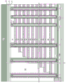
参考图3,阶梯式腔可形成于触点区300内,所述触点区定位于存储器阵列区100与包含用于外围电路的至少一个半导体装置的外围装置区200之间。阶梯式腔可具有各种阶梯式表面,使得阶梯式腔的水平横截面形状根据与衬底8的顶部表面的竖直距离而逐阶改变。在一个实施例中,阶梯式腔可通过反复执行一组处理步骤来形成。所述组处理步骤可包含例如将腔的深度竖直地增加一个或多个层级的第一类型的蚀刻过程,以及横向地扩展待在第一类型的后续蚀刻过程中竖直地蚀刻的区域的第二类型的蚀刻过程。如本文中所使用,包含交替的多个的结构的“层级”定义为所述结构内的一对第一材料层和第二材料层的相对位置。Referring to FIG. 3, a stepped cavity may be formed within a contact region 300 positioned between the memory array region 100 and the peripheral device region 200 including at least one semiconductor device for peripheral circuits. The stepped cavity may have various stepped surfaces such that the horizontal cross-sectional shape of the stepped cavity changes stepwise according to the vertical distance from the top surface of the substrate 8 . In one embodiment, the stepped cavity may be formed by repeatedly performing a set of processing steps. The set of processing steps may comprise, for example, a first type of etching process that vertically increases the depth of the cavity by one or more levels, and laterally expanding the area to be vertically etched in a subsequent etching process of the first type. The second type of etching process. As used herein, a "level" of a structure comprising alternating plurals is defined as the relative position of a pair of first and second material layers within the structure.

阶梯式表面通过形成阶梯式腔而形成于绝缘顶盖层70和交替堆叠(32、42)的外围部分处。如本文中所使用,“阶梯式表面”指代包含至少两个水平表面和至少两个竖直表面,使得每一水平表面邻接到从水平表面的第一边缘向上延伸的第一竖直表面,且邻接到从水平表面的第二边缘向下延伸的第二竖直表面的一组表面。“阶梯式腔”指代具有阶梯式表面的腔。Stepped surfaces are formed at the insulating cap layer 70 and peripheral portions of the alternating stacks (32, 42) by forming stepped cavities. As used herein, "stepped surface" refers to comprising at least two horizontal surfaces and at least two vertical surfaces, such that each horizontal surface abuts a first vertical surface extending upwardly from a first edge of the horizontal surface, and a set of surfaces adjacent to the second vertical surface extending downwardly from the second edge of the horizontal surface. "Stepped cavity" refers to a cavity having a stepped surface.

通过图案化绝缘顶盖层70和交替堆叠(32、42)而形成阶台区。交替堆叠(32、42)内除最顶部牺牲材料层42外的每一牺牲材料层42比交替堆叠(32、42)内的任何上覆牺牲材料层42横向延伸更远。阶台区包含从交替堆叠(32、42)内的最底部层连续延伸到交替堆叠(32、42)内的最顶部层的交替堆叠(32、42)的阶梯式表面。Step regions are formed by patterning the insulating capping layer 70 and alternating stacks (32, 42). Each sacrificial material layer 42 other than the topmost sacrificial material layer 42 within the alternating stack (32, 42) extends further laterally than any overlying sacrificial material layer 42 within the alternating stack (32, 42). The stepped region comprises a stepped surface of alternating stacks (32, 42) extending continuously from the bottommost layer within the alternating stack (32, 42) to the topmost layer within the alternating stack (32, 42).

逆向阶梯式电介质材料部分65(即,绝缘填充材料部分)可通过在阶梯式腔中沉积电介质材料而形成于阶梯式腔中。举例来说,例如氧化硅等电介质材料可沉积于阶梯式腔中。举例来说,可通过化学机械平坦化(CMP)从绝缘顶盖层70的最顶部表面上方移除沉积的电介质材料的过量部分。填充阶梯式腔的所沉积电介质材料的剩余部分构成逆向阶梯式电介质材料部分65。如本文中所使用,“逆向阶梯式”元件指代具有阶梯式表面和水平横截面积的元件,所述横截面积根据与上面存在元件的衬底的顶部表面的竖直距离单调地增加。如果氧化硅用于逆向阶梯式电介质材料部分65,那么逆向阶梯式电介质材料部分65的氧化硅可或不可掺杂有掺杂剂,如B、P和/或F。The reverse stepped dielectric material portion 65 (ie, the insulating fill material portion) may be formed in the stepped cavity by depositing a dielectric material in the stepped cavity. For example, a dielectric material such as silicon oxide can be deposited in the stepped cavity. For example, the excess portion of the deposited dielectric material may be removed from over the topmost surface of insulating cap layer 70 by chemical mechanical planarization (CMP). The remainder of the deposited dielectric material filling the stepped cavity constitutes the reverse stepped dielectric material portion 65 . As used herein, a "reverse stepped" element refers to an element having a stepped surface and a horizontal cross-sectional area that increases monotonically according to vertical distance from the top surface of the substrate on which the element resides. If silicon oxide is used for reverse stepped dielectric material portion 65, the silicon oxide of reverse stepped dielectric material portion 65 may or may not be doped with dopants, such as B, P, and/or F.

参考图4A、4B和5A,包含至少光致抗蚀剂层的光刻材料堆叠(未示出)可形成于绝缘顶盖层70上方,并且可以光刻方式图案化以在其中形成开口。所述开口包含形成于存储器阵列区100上方的第一组开口和形成于触点区300上方的第二组开口。光刻材料堆叠中的图案可通过采用经图案化光刻材料堆叠作为蚀刻掩模的至少一次各向异性蚀刻而转印通过绝缘顶盖层70、交替堆叠(32、42)和逆向阶梯式电介质材料部分65。4A, 4B and 5A, a stack of photoresist material (not shown) including at least a photoresist layer can be formed over the insulating cap layer 70 and can be photolithographically patterned to form openings therein. The openings include a first set of openings formed over the memory array region 100 and a second set of openings formed over the contact region 300 . The pattern in the lithographic material stack can be transferred through the insulating cap layer 70, the alternating stacks (32, 42) and the reverse stepped dielectric by at least one anisotropic etch using the patterned lithographic material stack as an etch mask Material section 65.

下伏于存储器阵列区100内的经图案化光刻材料堆叠中的开口的绝缘顶盖层70和交替堆叠(32、42)的部分被蚀刻以形成存储器开口49。下伏于触点区300内的经图案化光刻材料堆叠中的开口的绝缘顶盖层70、交替堆叠(32、42)和逆向阶梯式电介质材料部分65的部分被蚀刻以形成支撑开口19。如本文所使用,“存储器开口”指代其中随后形成例如存储器堆叠结构等存储器元件的结构。如本文所使用,“支撑开口”指代其中随后形成机械地支撑其它元件的支撑结构(例如支撑柱结构)的结构。Portions of the insulating cap layer 70 and alternating stacks ( 32 , 42 ) underlying openings in the patterned stack of photolithographic material within the memory array region 100 are etched to form memory openings 49 . Portions of insulating cap layer 70 , alternating stacks ( 32 , 42 ) and reverse stepped dielectric material portions 65 underlying openings in the patterned photolithographic material stack within contact region 300 are etched to form support openings 19 . As used herein, "memory opening" refers to a structure in which memory elements, such as memory stack structures, are subsequently formed. As used herein, "support opening" refers to a structure in which support structures (eg, support post structures) that mechanically support other elements are subsequently formed.

存储器开口49延伸穿过整个交替堆叠(32、42)。支撑开口19延伸穿过交替堆叠(32、42)内的层的子组。用以蚀刻穿过交替堆叠(32、42)的材料的各向异性蚀刻过程的化学作用可交替以优化交替堆叠(32、42)中的第一材料和第二材料的蚀刻。各向异性蚀刻可为例如一系列反应性离子蚀刻。存储器开口49和支撑开口19的侧壁可为基本上竖直的,或可为锥形的。图案化光刻材料堆叠可随后例如通过灰化来移除。Memory openings 49 extend through the entire alternating stack (32, 42). The support openings 19 extend through subsets of layers within the alternating stack (32, 42). The chemistry of the anisotropic etching process used to etch through the material of the alternating stacks (32, 42) can be alternated to optimize the etching of the first and second materials in the alternating stacks (32, 42). The anisotropic etching can be, for example, a series of reactive ion etchings. The side walls of the reservoir opening 49 and the support opening 19 may be substantially vertical, or may be tapered. The patterned lithographic material stack can then be removed, eg, by ashing.

存储器开口49和支撑开口19可从绝缘顶盖层70的顶部表面延伸到处理中源极层级材料层10中的下部源极层级材料层112。在一个实施例中,在每一存储器开口49和每一支撑开口19的底部处物理上暴露下部源极层级材料层112的顶部表面之后可以任选地执行进入下部源极层级材料层112的过度蚀刻。凹部深度可例如介于从1nm到50nm的范围内,但也可采用更小和更大的凹部深度。过度蚀刻是任选的,且可省略。如果未执行过度蚀刻,那么存储器开口49和支撑开口19的底部表面可与下部源极层级材料层112的最顶部表面共面。The memory opening 49 and the support opening 19 may extend from the top surface of the insulating cap layer 70 to the lower source level material layer 112 in the processing source level material layer 10 . In one embodiment, transition into the lower source level material layer 112 may optionally be performed after physically exposing the top surface of the lower source level material layer 112 at the bottom of each memory opening 49 and each support opening 19 etching. The recess depth may for example be in the range from 1 nm to 50 nm, although smaller and larger recess depths may also be employed. Overetching is optional and can be omitted. If no overetch is performed, the bottom surfaces of the memory openings 49 and the support openings 19 may be coplanar with the topmost surface of the lower source level material layer 112 .

存储器开口49和支撑开口19中的每一个可以包含基本上垂直于衬底的最顶部表面延伸的侧壁(或多个侧壁)。可在存储器阵列区100中形成存储器开口49的二维阵列。可在触点区300中形成支撑开口19的二维阵列。Each of memory opening 49 and support opening 19 may include a sidewall (or sidewalls) extending substantially perpendicular to the topmost surface of the substrate. A two-dimensional array of memory openings 49 may be formed in memory array region 100 . A two-dimensional array of support openings 19 may be formed in the contact region 300 .

存储器开口49可以布置成群组,使得每个群组包含多行存储器开口49。在存储器开口49的每个群组内,存储器开口49可以布置成沿着第一水平方向hd1延伸的行。多个行可以沿着垂直于第一水平方向hd1的第二水平方向hd2间隔开,存储器开口49的整个群组具有均匀的行间间距。在此情况下,各行存储器开口49沿着第二水平方向“在间距上(on-pitch)”,即,具有均匀间距。在一个实施例中,存储器开口可布置成包含多行存储器开口49的集群,即,群组。在一个实施例中,集群中的存储器开口49可被布置成具有二维周期性的二维六边形阵列。The memory openings 49 may be arranged in groups such that each group contains multiple rows of memory openings 49 . Within each group of the memory openings 49, the memory openings 49 may be arranged in rows extending along the first horizontal direction hd1. A plurality of rows may be spaced apart along a second horizontal direction hd2 perpendicular to the first horizontal direction hd1, and the entire group of memory openings 49 has a uniform inter-row spacing. In this case, each row of memory openings 49 is "on-pitch" along the second horizontal direction, ie, has a uniform pitch. In one embodiment, the memory openings may be arranged in clusters, ie, groups, comprising rows of memory openings 49 . In one embodiment, the memory openings 49 in the cluster may be arranged in a two-dimensional hexagonal array with two-dimensional periodicity.

参考图5B,可在存储器开口49中和支撑开口19中循序地沉积连续存储器膜50L和半导体通道材料层611L。每一连续存储器膜50L可包含层堆叠,其包含连续阻挡电介质层52L、连续电荷存储层54L和连续隧穿电介质层56L。连续存储器膜50L连续延伸进入每一存储器开口49并进入每一支撑开口19。Referring to FIG. 5B , a continuous memory film 50L and a layer of semiconductor channel material 611L may be sequentially deposited in the memory openings 49 and in the support openings 19 . Each continuous memory film 50L may include a layer stack including a continuous blocking dielectric layer 52L, a continuous charge storage layer 54L, and a continuous tunneling dielectric layer 56L. The continuous memory film 50L extends continuously into each memory opening 49 and into each support opening 19 .

连续阻挡电介质层52L可包含单个电介质材料层或多个电介质材料层的堆叠。在一个实施例中,阻挡电介质层可包含基本上由电介质金属氧化物组成的电介质金属氧化物层。如本文中所使用,电介质金属氧化物是指包含至少一种金属元素和至少氧的电介质材料。电介质金属氧化物可主要由所述至少一种金属元素和氧组成,或可主要由所述至少一种金属元素、氧以及至少一种非金属元素(例如氮)组成。在一个实施例中,连续阻挡电介质层52L可包含具有大于7.9的介电常数的电介质金属氧化物,即,具有大于氮化硅的介电常数的介电常数。The continuous blocking dielectric layer 52L may comprise a single layer of dielectric material or a stack of multiple layers of dielectric material. In one embodiment, the blocking dielectric layer may comprise a dielectric metal oxide layer consisting essentially of a dielectric metal oxide. As used herein, a dielectric metal oxide refers to a dielectric material comprising at least one metal element and at least oxygen. The dielectric metal oxide may consist essentially of the at least one metal element and oxygen, or may consist essentially of the at least one metal element, oxygen, and at least one non-metal element (eg, nitrogen). In one embodiment, the continuous blocking dielectric layer 52L may include a dielectric metal oxide having a dielectric constant greater than 7.9, ie, having a dielectric constant greater than that of silicon nitride.

电介质金属氧化物的非限制性实例包含氧化铝(Al2O3)、氧化铪(HfO2)、氧化镧(LaO2)、氧化钇(Y2O3)、氧化钽(Ta2O5)、其硅酸盐、其氮掺杂化合物、其合金以及其堆叠。电介质金属氧化物层可例如通过化学气相沉积(CVD)、原子层沉积(ALD)、脉冲激光沉积(PLD)、液体源雾化化学沉积或其组合而沉积。电介质金属氧化物层的厚度可在1nm到20nm的范围内,但是也可采用更小和更大的厚度。电介质金属氧化物层可随后充当阻挡所存储电荷泄漏到控制栅极电极的电介质材料部分。在一个实施例中,连续阻挡电介质层52L包含氧化铝。在一个实施例中,连续阻挡电介质层52L可包含具有不同材料组成物的多个电介质金属氧化层。Non-limiting examples of dielectric metal oxides include aluminum oxide (Al 2 O 3 ), hafnium oxide (HfO 2 ), lanthanum oxide (LaO 2 ), yttrium oxide (Y 2 O 3 ), tantalum oxide (Ta 2 O 5 ) , its silicates, its nitrogen-doped compounds, its alloys, and its stacks. The dielectric metal oxide layer can be deposited, for example, by chemical vapor deposition (CVD), atomic layer deposition (ALD), pulsed laser deposition (PLD), liquid source atomized chemical deposition, or a combination thereof. The thickness of the dielectric metal oxide layer may range from 1 nm to 20 nm, although smaller and larger thicknesses may also be employed. The dielectric metal oxide layer may then act as a portion of the dielectric material that blocks leakage of the stored charge to the control gate electrode. In one embodiment, the continuous blocking dielectric layer 52L comprises aluminum oxide. In one embodiment, the continuous blocking dielectric layer 52L may comprise multiple dielectric metal oxide layers having different material compositions.

替代或另外地,连续阻挡电介质层52L可包含电介质半导体化合物,如氧化硅、氮氧化硅、氮化硅或其组合。在一个实施例中,连续阻挡电介质层52L可包含氧化硅。在此情况下,连续阻挡电介质层52L的电介质半导体化合物可通过保形沉积方法形成,例如低压化学气相沉积、原子层沉积或其组合。电介质半导体化合物的厚度可在1nm到20nm的范围内,但也可采用更小和更大厚度。或者,可省略连续阻挡电介质层52L,且背侧阻挡电介质层可在随后待形成的存储器膜的表面上形成背侧凹部之后形成。Alternatively or additionally, the continuous blocking dielectric layer 52L may comprise a dielectric semiconductor compound, such as silicon oxide, silicon oxynitride, silicon nitride, or combinations thereof. In one embodiment, the continuous blocking dielectric layer 52L may comprise silicon oxide. In this case, the dielectric semiconductor compound of the continuous blocking dielectric layer 52L may be formed by a conformal deposition method, such as low pressure chemical vapor deposition, atomic layer deposition, or a combination thereof. The thickness of the dielectric semiconductor compound may be in the range of 1 nm to 20 nm, although smaller and larger thicknesses may also be employed. Alternatively, the continuous blocking dielectric layer 52L may be omitted, and the backside blocking dielectric layer may be formed after the backside recesses are formed on the surface of the memory film to be formed later.

随后,可形成连续电荷存储层54L。在一个实施例中,连续电荷存储层54L可为电荷捕获材料的连续层或经图案化离散部分,所述电荷捕获材料包含可例如为氮化硅的电介质电荷捕获材料。替代地,例如通过形成于进入牺牲材料层42的橫向凹部内,连续电荷存储层54L可包含导电材料的连续层或经图案化离散部分,例如经图案化为多个电隔离部分(例如,浮动栅极)的掺杂多晶硅或金属材料。在一个实施例中,连续电荷存储层54L包含氮化硅层。在一个实施例中,牺牲材料层42和绝缘层32可具有竖直重合的侧壁,且连续电荷存储层54L可形成为单个连续层。如本文中所使用,如果第二表面上覆于或下伏于第一表面,并且如果存在包含第一表面和第二表面的竖直平面,那么第一表面和第二表面“竖直重合”。Subsequently, the continuous charge storage layer 54L may be formed. In one embodiment, the continuous charge storage layer 54L may be a continuous layer or patterned discrete portions of charge trapping material including a dielectric charge trapping material, which may be, for example, silicon nitride. Alternatively, such as by being formed within lateral recesses into sacrificial material layer 42, continuous charge storage layer 54L may comprise a continuous layer of conductive material or patterned discrete portions, such as patterned into a plurality of electrically isolated portions (eg, floating gate) of doped polysilicon or metal materials. In one embodiment, the continuous charge storage layer 54L includes a silicon nitride layer. In one embodiment, sacrificial material layer 42 and insulating layer 32 may have vertically overlapping sidewalls, and continuous charge storage layer 54L may be formed as a single continuous layer. As used herein, a first surface and a second surface "vertically coincide" if the second surface overlies or underlies the first surface, and if there is a vertical plane that includes the first surface and the second surface .

在另一实施例中,牺牲材料层42可相对于绝缘层32的侧壁横向凹入,且可采用沉积过程和各向异性蚀刻过程的组合将连续电荷存储层54L形成为竖直间隔开的多个存储器材料部分。虽然采用其中连续电荷存储层54L为单个连续层的实施例描述本公开,但本文明确地预期其中连续电荷存储层54L被竖直隔开的多个存储器材料部分(其可为电荷捕获材料部分或电隔离导电材料部分)替换的实施例。In another embodiment, sacrificial material layer 42 may be recessed laterally relative to the sidewalls of insulating layer 32, and a combination of deposition and anisotropic etching processes may be employed to form continuous charge storage layer 54L as vertically spaced apart Multiple memory material sections. Although the present disclosure is described with embodiments in which the continuous charge storage layer 54L is a single continuous layer, multiple portions of memory material (which may be portions of charge trapping material or Electrically isolated conductive material portion) alternative embodiment.

连续电荷存储层54L可形成为均质组成的单个电荷存储层,或可包含多个电荷存储层的堆叠。所述多个电荷存储层(如果采用的话)可包括含有导电材料(例如,比如钨、钼、钽、钛、铂、钌及其合金等金属,或比如硅化钨、硅化钼、硅化钽、硅化钛、硅化镍、硅化钴或其组合等金属硅化物)和/或半导体材料(例如,包含至少一种元素半导体元件的多晶或非晶形半导体材料,或至少一种化合物半导体材料)的多个间隔开的浮动栅极材料层。替代地或另外,连续电荷存储层54L可以包括绝缘电荷捕获材料,例如一个或多个氮化硅片段。或者,连续电荷存储层54L可包括例如金属纳米粒子等导电纳米粒子,所述金属纳米粒子可以是例如钌纳米粒子。连续电荷存储层54L可例如通过化学气相沉积(CVD)、原子层沉积(ALD)、物理气相沉积(PVD)或用于在其中存储电荷的任何适合的沉积技术而形成。连续电荷存储层54L的厚度可在2nm到20nm的范围内,但也可采用更小和更大厚度。The continuous charge storage layer 54L may be formed as a single charge storage layer of homogeneous composition, or may comprise a stack of multiple charge storage layers. The plurality of charge storage layers, if employed, may include metals containing conductive materials (eg, metals such as tungsten, molybdenum, tantalum, titanium, platinum, ruthenium, and alloys thereof, or metals such as tungsten, molybdenum, tantalum, silicide) a plurality of metal silicides such as titanium, nickel silicide, cobalt silicide, or combinations thereof) and/or semiconductor materials (eg, polycrystalline or amorphous semiconductor materials comprising at least one elemental semiconductor element, or at least one compound semiconductor material) spaced apart layers of floating gate material. Alternatively or additionally, the continuous charge storage layer 54L may include an insulating charge trapping material, such as one or more silicon nitride segments. Alternatively, the continuous charge storage layer 54L may include conductive nanoparticles, such as metal nanoparticles, which may be, for example, ruthenium nanoparticles. Continuous charge storage layer 54L may be formed, for example, by chemical vapor deposition (CVD), atomic layer deposition (ALD), physical vapor deposition (PVD), or any suitable deposition technique for storing charge therein. The thickness of the continuous charge storage layer 54L may range from 2 nm to 20 nm, although smaller and larger thicknesses may also be employed.

连续隧穿电介质层56L包含电介质材料,电荷隧穿可穿过所述电介质材料在适合的电偏压条件下执行。取决于要形成的单片三维NAND串存储器装置的操作模式,可通过热载流子注入或通过佛勒-诺德海姆(Fowler-Nordheim)隧穿引发电荷转移来执行电荷隧穿。连续隧穿电介质层56L可包含氧化硅、氮化硅、氮氧化硅、电介质金属氧化物(例如氧化铝和二氧化铪)、电介质金属氮氧化物、电介质金属硅酸盐、其合金,和/或其组合。在一个实施例中,连续隧穿电介质层56L可包含第一氧化硅层、氮氧化硅层以及第二氧化硅层的堆叠,所述堆叠通常称为ONO堆叠。在一个实施例中,连续隧穿电介质层56L可包含大体上不含碳的氧化硅层或大体上不含碳的氮氧化硅层。连续隧穿电介质层56L的厚度可在2nm到20nm的范围内,但也可采用更小和更大厚度。The continuous tunneling dielectric layer 56L includes a dielectric material through which charge tunneling can be performed under suitable electrical bias conditions. Depending on the mode of operation of the monolithic three-dimensional NAND string memory device to be formed, charge tunneling can be performed by hot carrier injection or by induced charge transfer by Fowler-Nordheim tunneling. The continuous tunneling dielectric layer 56L may comprise silicon oxide, silicon nitride, silicon oxynitride, dielectric metal oxides (eg, aluminum oxide and hafnium dioxide), dielectric metal oxynitrides, dielectric metal silicates, alloys thereof, and/or or a combination thereof. In one embodiment, the continuous tunneling dielectric layer 56L may include a stack of a first silicon oxide layer, a silicon oxynitride layer, and a second silicon dioxide layer, commonly referred to as an ONO stack. In one embodiment, the continuous tunneling dielectric layer 56L may comprise a substantially carbon-free silicon oxide layer or a substantially carbon-free silicon oxynitride layer. The thickness of the continuous tunneling dielectric layer 56L may be in the range of 2 nm to 20 nm, although smaller and larger thicknesses may also be employed.

半导体通道材料层611L包含半导体材料,如至少一种元素半导体材料、至少一种III-V化合物半导体材料、至少一种II-VI化合物半导体材料、至少一种有机半导体材料或本领域中已知的其它半导体材料。在一个实施例中,半导体通道材料层611L包含非晶硅或多晶硅。半导体通道材料层611L可通过例如低压化学气相沉积(LPCVD)的保形沉积方法形成。半导体通道材料层611L的厚度可介于从2nm到20nm的范围内,但是也可采用更小和更大的厚度。半导体通道材料层611L可具有介于从1.0x 10¹⁴/cm3到3.0x 1017/cm3的范围内的掺杂剂浓度的第一导电性类型的掺杂。存储器腔49'形成于每一存储器开口49的未填充有沉积材料层(50L、611L)的体积中。The semiconductor channel material layer 611L comprises a semiconductor material, such as at least one elemental semiconductor material, at least one III-V compound semiconductor material, at least one II-VI compound semiconductor material, at least one organic semiconductor material, or as known in the art other semiconductor materials. In one embodiment, the semiconductor channel material layer 611L includes amorphous silicon or polysilicon. The semiconductor channel material layer 611L may be formed by a conformal deposition method such as low pressure chemical vapor deposition (LPCVD). The thickness of the semiconductor channel material layer 611L may range from 2 nm to 20 nm, although smaller and larger thicknesses may also be employed. The semiconductor channel material layer 611L may have doping of the first conductivity type with a dopant concentration ranging from 1.0×10 14 /cm 3 to 3.0×10 17 /cm 3 . A memory cavity 49' is formed in the volume of each memory opening 49 that is not filled with a layer of deposited material (50L, 611L).

参考图5C,例如未掺杂硅酸盐玻璃、掺杂硅酸盐玻璃或有机硅酸盐玻璃等电介质材料可通过保形或非保形沉积方法沉积于存储器腔49'和支撑开口19的未填充体积中。电介质材料可通过凹部蚀刻过程竖直凹入,使得电介质材料的剩余部分在包含绝缘顶盖层70的顶部表面的水平平面与包含绝缘顶盖层70的底部表面的水平平面之间具有顶部表面。电介质材料的每一剩余部分构成电介质芯62。凹部腔存在于每一电介质芯62上方。Referring to FIG. 5C , a dielectric material such as undoped silicate glass, doped silicate glass, or organosilicate glass can be deposited on the memory cavity 49 ′ and the unfinished portion of the support opening 19 by conformal or non-conformal deposition methods. fill volume. The dielectric material may be vertically recessed by a recess etch process such that the remainder of the dielectric material has a top surface between the horizontal plane containing the top surface of insulating cap layer 70 and the horizontal plane containing the bottom surface of insulating cap layer 70 . Each remaining portion of the dielectric material constitutes a dielectric core 62 . A recess cavity exists above each dielectric core 62 .

参考图5D、6A、6B和6C,牺牲材料部分612可通过牺牲材料的沉积而形成于凹部腔中。在一个实施例中,牺牲材料可为具有第一导电性类型的掺杂的半导体材料,第一导电性类型即半导体通道材料层611L的导电性类型。可从包含绝缘顶盖层70的顶部表面的水平平面上方移除牺牲材料的过量部分和连续存储器膜50L的水平部分。牺牲材料的每一剩余部分构成牺牲材料部分612。在一个实施例中,牺牲材料部分612可包含具有第一导电性类型的掺杂的多晶硅或非晶硅。位于相应存储器开口49中或相应支撑开口19中的半导体通道材料层611L的每一剩余部分构成竖直半导体通道611。位于相应存储器开口49中或相应支撑开口19中的连续存储器膜50L的每一剩余部分构成存储器膜50。Referring to Figures 5D, 6A, 6B and 6C, a sacrificial material portion 612 may be formed in the recess cavity by deposition of a sacrificial material. In one embodiment, the sacrificial material may be a doped semiconductor material having a first conductivity type, ie, the conductivity type of the semiconductor channel material layer 611L. The excess portion of the sacrificial material and the horizontal portion of the continuous memory film 50L may be removed from above the horizontal plane containing the top surface of the insulating cap layer 70 . Each remaining portion of the sacrificial material constitutes a sacrificial material portion 612 . In one embodiment, the sacrificial material portion 612 may comprise doped polysilicon or amorphous silicon having a first conductivity type. Each remaining portion of the layer of semiconductor channel material 611L located in the corresponding memory opening 49 or in the corresponding support opening 19 constitutes a vertical semiconductor channel 611 . Each remaining portion of the continuous memory film 50L located in the corresponding memory opening 49 or in the corresponding support opening 19 constitutes the memory film 50 .

连续阻挡电介质层52L的每一离散剩余部分构成阻挡电介质层52。连续电荷存储层54L的每一离散剩余部分构成电荷存储层54。连续隧穿电介质层56L的每一离散剩余部分构成隧穿电介质层56。邻接的每一组阻挡电介质层52、电荷存储层54和隧穿电介质层56共同构成存储器膜50,所述存储器膜可以宏观滞留时间存储电荷。在一些实施例中,阻挡电介质层52在此步骤可能不存在于存储器膜50中,且阻挡电介质层可以随后在背侧凹部的形成之后形成。如本文所使用,宏观滞留时间指代适合于存储器装置作为永久存储器装置操作的滞留时间,例如超过24小时的滞留时间。Each discrete remaining portion of continuous blocking dielectric layer 52L constitutes blocking dielectric layer 52 . Each discrete remaining portion of continuous charge storage layer 54L constitutes charge storage layer 54 . Each discrete remaining portion of the continuous tunneling dielectric layer 56L constitutes the tunneling dielectric layer 56 . Each adjacent set of blocking dielectric layer 52, charge storage layer 54, and tunneling dielectric layer 56 collectively constitutes a memory film 50 that can store charge for a macroscopic residence time. In some embodiments, the blocking dielectric layer 52 may not be present in the memory film 50 at this step, and the blocking dielectric layer may be formed subsequently after the formation of the backside recess. As used herein, macroscopic residence time refers to a residence time suitable for operation of a memory device as a persistent memory device, eg, a residence time in excess of 24 hours.

竖直半导体通道611和存储器开口49中的存储器膜50的每一邻接组合构成存储器堆叠结构55。每一存储器堆叠结构55穿过交替堆叠(32、42)形成。存储器堆叠结构55、电介质芯62和牺牲材料部分612的每一邻接组合填充相应存储器开口49,且构成存储器开口填充结构58。存储器膜50、竖直半导体通道601、电介质芯62和填充支撑开口19的牺牲材料部分612的每一邻接组合构成支撑开口填充结构20。存储器堆叠结构55可布置成集群。在一个实施例中,集群中的存储器堆叠结构55可被布置成具有二维周期性的二维六边形阵列。Each adjoining combination of the vertical semiconductor channel 611 and the memory film 50 in the memory opening 49 constitutes the memory stack structure 55 . Each memory stack structure 55 is formed through alternating stacks (32, 42). Each adjoining combination of memory stack structure 55 , dielectric core 62 , and sacrificial material portion 612 fills corresponding memory opening 49 and constitutes memory opening filling structure 58 . Each adjoining combination of memory film 50 , vertical semiconductor channel 601 , dielectric core 62 , and sacrificial material portion 612 filling support opening 19 constitutes support opening fill structure 20 . Memory stacks 55 may be arranged in clusters. In one embodiment, the memory stacks 55 in the cluster may be arranged in a two-dimensional hexagonal array with two-dimensional periodicity.

参考图7A和7B,平坦绝缘间隔物层71、电介质蚀刻终止层73、电介质衬里75和牺牲填充材料层81依序形成于绝缘顶盖层70、存储器开口填充结构58和支撑开口填充结构20的顶部表面上。平坦绝缘间隔物层71包含例如氧化硅的电介质材料,且可具有介于从20nm到200nm的范围内的厚度,但是也可采用更小和更大的厚度。电介质蚀刻终止层73包含可在牺牲填充材料层81的后续图案化期间充当蚀刻终止材料的电介质材料。在一个实施例中,电介质蚀刻终止层73可包含例如氧化铝的电介质金属氧化物。电介质蚀刻终止层73的厚度可介于从2nm到50nm的范围内,但也可采用更小和更大的厚度。电介质衬里75包含例如氧化硅的电介质材料,且可具有介于从2nm到50nm的范围内的厚度,但是也可采用更小和更大的厚度。牺牲填充材料层81包含与电介质蚀刻终止层73和电介质衬里75的材料不同的材料。举例来说,牺牲填充材料层81可包含氮化硅。牺牲填充材料层81的厚度可介于从20nm到400nm的范围内,例如从40nm到200nm,但是也可采用更小和更大的厚度。7A and 7B, a planar insulating spacer layer 71, a dielectric etch stop layer 73, a dielectric liner 75 and a sacrificial filling material layer 81 are sequentially formed on the insulating cap layer 70, the memory opening filling structure 58 and the supporting opening filling structure 20. on the top surface. The flat insulating spacer layer 71 comprises a dielectric material such as silicon oxide, and may have a thickness ranging from 20 nm to 200 nm, although smaller and larger thicknesses may also be employed. Dielectric etch stop layer 73 includes a dielectric material that can act as an etch stop material during subsequent patterning of sacrificial fill material layer 81 . In one embodiment, the dielectric etch stop layer 73 may comprise a dielectric metal oxide such as aluminum oxide. The thickness of the dielectric etch stop layer 73 may range from 2 nm to 50 nm, although smaller and larger thicknesses may also be employed. Dielectric liner 75 comprises a dielectric material such as silicon oxide, and may have a thickness ranging from 2 nm to 50 nm, although smaller and larger thicknesses may also be employed. Sacrificial fill material layer 81 contains a different material than that of dielectric etch stop layer 73 and dielectric liner 75 . For example, the sacrificial fill material layer 81 may include silicon nitride. The thickness of the sacrificial filler material layer 81 may range from 20 nm to 400 nm, eg, from 40 nm to 200 nm, although smaller and larger thicknesses may also be employed.

参考图8,牺牲填充材料层81经图案化以形成层81中的轨道形沟槽82。举例来说,光致抗蚀剂层(未示出)可施加于层81上方且以光刻方式图案化以在其中形成线图案。通过各向异性蚀刻过程,线图案光致抗蚀剂层转印通过层81和电介质衬里75以形成轨道形沟槽82。电介质蚀刻终止层73在沟槽82的形成期间充当蚀刻终止层结构。沟槽82沿着第一水平方向hd1横向延伸且具有沿着第二水平方向hd2的10到30nm的均匀宽度,例如15到20nm。沟槽82沿着第二水平方向hd2横向隔开。Referring to FIG. 8 , a layer 81 of sacrificial fill material is patterned to form track-shaped trenches 82 in layer 81 . For example, a photoresist layer (not shown) may be applied over layer 81 and lithographically patterned to form a line pattern therein. Through an anisotropic etching process, a line pattern photoresist layer is transferred through layer 81 and dielectric liner 75 to form track-shaped trenches 82 . Dielectric etch stop layer 73 acts as an etch stop layer structure during formation of trench 82 . The trenches 82 extend laterally along the first horizontal direction hd1 and have a uniform width along the second horizontal direction hd2 of 10 to 30 nm, eg, 15 to 20 nm. The trenches 82 are laterally spaced along the second horizontal direction hd2.

参考图9,牺牲衬里175可在轨道形沟槽82中沉积于层81的顶部表面和侧壁上以及电介质蚀刻终止层73的在沟槽82中物理上暴露的部分的顶部表面上。牺牲衬里175包含与电介质蚀刻终止层73的材料不同的材料。举例来说,牺牲衬里175可包含氧化硅。牺牲衬里175的厚度可介于从1nm到20nm的范围内,例如从2nm到10nm,但是也可采用更小和更大的厚度。Referring to FIG. 9 , sacrificial liner 175 may be deposited in track-shaped trench 82 on the top surface and sidewalls of layer 81 and on the top surface of the portion of dielectric etch stop layer 73 that is physically exposed in trench 82 . Sacrificial liner 175 contains a different material than that of dielectric etch stop layer 73 . For example, the sacrificial liner 175 may include silicon oxide. The thickness of the sacrificial liner 175 may range from 1 nm to 20 nm, eg, from 2 nm to 10 nm, although smaller and larger thicknesses may also be employed.

参考图10A和10B,模板轨道结构77形成于位于牺牲填充材料层81内部的轨道形沟槽82中的牺牲衬里175上。模板轨道结构77可形成于通过牺牲填充材料层81彼此横向隔开的多个离散部分中。模板轨道结构77可例如通过在沟槽82中沉积牺牲材料且通过采用牺牲衬里175的顶部表面作为终止结构使牺牲材料平坦化而形成。随后使用选择性蚀刻使模板轨道结构77凹入牺牲衬里175和层81的顶部表面下方以形成轨道形凹部84。举例来说,模板轨道结构77可包含氮化硅。在此情况下,所述选择性蚀刻可为与牺牲衬里175相比选择性地蚀刻模板轨道结构77的热磷酸蚀刻。模板轨道结构可为约100到200nm高和约15到40nm宽,例如20与30nm之间宽。Referring to FIGS. 10A and 10B , template rail structures 77 are formed on sacrificial liners 175 in rail-shaped trenches 82 inside sacrificial fill material layer 81 . Template track structures 77 may be formed in a plurality of discrete portions laterally separated from each other by layers of sacrificial fill material 81 . Template track structure 77 may be formed, for example, by depositing a sacrificial material in trench 82 and planarizing the sacrificial material using the top surface of sacrificial liner 175 as a termination structure. The template rail structures 77 are then recessed under the top surfaces of the sacrificial liner 175 and layer 81 using selective etching to form rail-shaped recesses 84 . For example, template track structure 77 may comprise silicon nitride. In this case, the selective etch may be a hot phosphoric acid etch that selectively etches template track structure 77 compared to sacrificial liner 175 . The template orbital structure may be about 100 to 200 nm high and about 15 to 40 nm wide, eg, between 20 and 30 nm wide.

参考图11,电介质顶盖275形成于模板轨道结构77上方和牺牲填充材料层81上方的轨道形凹部84中。电介质顶盖275可以包括与模板轨道结构77和牺牲填充材料层81的材料不同的电介质材料。举例来说,如果模板轨道结构77和牺牲填充材料层81包括氮化硅,那么电介质顶盖275可包括氧化硅。电介质顶盖275可以通过反应性离子蚀刻或CMP而平坦化。由于凹部84的存在,位于模板轨道结构77上方的电介质顶盖275的第一部分275A比位于牺牲填充材料层81上方的电介质顶盖275的第二部分275B更厚。举例来说,第一部分275A可以比第二部分275B厚50%到300%。第一部分275A可以是20到50nm厚,而第二部分275B可以是5到20nm厚。Referring to FIG. 11 , dielectric caps 275 are formed in track-shaped recesses 84 over template track structures 77 and over sacrificial fill material layer 81 . Dielectric cap 275 may include a different dielectric material than that of template track structure 77 and sacrificial fill material layer 81 . For example, if template track structure 77 and sacrificial fill material layer 81 include silicon nitride, dielectric cap 275 may include silicon oxide. The dielectric cap 275 may be planarized by reactive ion etching or CMP. The first portion 275A of the dielectric cap 275 over the template track structure 77 is thicker than the second portion 275B of the dielectric cap 275 over the sacrificial fill material layer 81 due to the presence of the recess 84 . For example, the first portion 275A may be 50% to 300% thicker than the second portion 275B. The first portion 275A may be 20 to 50 nm thick, and the second portion 275B may be 5 to 20 nm thick.

参考图12A和12B,漏极选择层级开口149穿过模板轨道结构77、牺牲衬里175、电介质顶盖275和牺牲填充材料层81的组合形成。漏极选择层级开口149可具有与存储器开口49相同的图案,且因此,可具有与存储器开口填充结构58相同的图案。在一个实施例中,漏极选择层级开口149可具有圆柱形形状,在此情况下漏极选择层级开口149可为漏极选择层级圆柱形开口。Referring to FIGS. 12A and 12B , drain select level openings 149 are formed through the combination of template track structure 77 , sacrificial liner 175 , dielectric cap 275 and sacrificial fill material layer 81 . Drain select level openings 149 may have the same pattern as memory openings 49 , and thus, may have the same pattern as memory opening fill structures 58 . In one embodiment, the drain select level opening 149 may have a cylindrical shape, in which case the drain select level opening 149 may be a drain select level cylindrical opening.

漏极选择层级开口149可包含延伸穿过牺牲衬里175的竖直部分和电介质顶盖275的第一部分275A的漏极选择层级开口149的第一子组,以及不延伸穿过牺牲衬里175的竖直部分和电介质顶盖275的第一部分275A的漏极选择层级开口149的第二子组。漏极选择层级开口149的第一子组延伸穿过模板轨道结构77中的相应一个和牺牲填充材料层81的一部分。漏极选择层级开口149的第二子组与模板轨道结构77横向隔开,延伸穿过电介质顶盖275的第二部分275B且完全形成于牺牲填充材料层81的区域内。Drain select level openings 149 may include a first subset of drain select level openings 149 extending through vertical portions of sacrificial liner 175 and first portion 275A of dielectric cap 275 , and vertical portions that do not extend through sacrificial liner 175 . The straight portion and the drain of the first portion 275A of the dielectric cap 275 select the second subset of level openings 149 . A first subset of drain select level openings 149 extend through a respective one of template track structures 77 and a portion of sacrificial fill material layer 81 . A second subset of drain select level openings 149 are laterally spaced apart from template track structure 77 , extend through second portion 275B of dielectric cap 275 and are formed entirely within the region of sacrificial fill material layer 81 .

在一个实施例中,沿着第一水平方向hd1延伸的模板轨道结构77的每一侧壁可由相应行的漏极选择层级开口149穿孔。沿着第一水平方向hd1延伸的模板轨道结构77的每一侧壁可包含平坦竖直侧壁片段和凹竖直侧壁片段的横向交替序列。如本文所使用,平坦竖直侧壁片段指代位于竖直二维平面内的侧壁片段。如本文所使用,凹竖直侧壁片段指代位于圆柱形表面的一部分内的侧壁片段,所述部分具有在水平平面内的曲率且沿着竖直方向笔直延伸。In one embodiment, each sidewall of the template track structure 77 extending along the first horizontal direction hd1 may be perforated by the drain selection level openings 149 of the corresponding row. Each sidewall of the template track structure 77 extending along the first horizontal direction hd1 may comprise a laterally alternating sequence of flat vertical sidewall segments and concave vertical sidewall segments. As used herein, a flat vertical sidewall segment refers to a sidewall segment that lies in a vertical two-dimensional plane. As used herein, a concave vertical sidewall segment refers to a sidewall segment located within a portion of a cylindrical surface that has a curvature in a horizontal plane and extends straight in a vertical direction.

在一个实施例中,漏极选择层级开口149可布置成沿着第一水平方向hd1延伸的行,且行到行间距p可以对于每一相邻对的漏极选择层级开口149的行是相同的。在一个实施例中,漏极选择层级开口149被布置成二维六边形阵列,且存储器堆叠结构55被布置成具有以漏极选择层级开口149的二维六边形阵列相同的二维周期性的另一二维六边形阵列。In one embodiment, the drain selection level openings 149 may be arranged in rows extending along the first horizontal direction hd1, and the row-to-row spacing p may be the same for each adjacent pair of rows of drain selection level openings 149 . In one embodiment, the drain select level openings 149 are arranged in a two-dimensional hexagonal array, and the memory stack structures 55 are arranged to have the same two-dimensional period as the two-dimensional hexagonal array of drain select level openings 149 Another two-dimensional hexagonal array of properties.

参考图13A和13B,沉积且各向异性蚀刻保形电介质材料层以在漏极选择层级开口149的侧壁上形成圆柱形电介质间隔物78。圆柱形电介质间隔物78形成于漏极选择层级开口149中的每一个内。圆柱形电介质间隔物78包含例如氧化硅的电介质材料。圆柱形电介质间隔物78可具有均匀橫向厚度,其可介于从1nm到20nm的范围内,例如从2nm到10nm。圆柱形电介质间隔物78在拓扑上与环面同胚,即,可以连续地拉伸为环面的形状而无需形成额外孔或破坏现有孔。Referring to FIGS. 13A and 13B , a layer of conformal dielectric material is deposited and anisotropically etched to form cylindrical dielectric spacers 78 on the sidewalls of drain select level openings 149 . Cylindrical dielectric spacers 78 are formed within each of the drain select level openings 149 . Cylindrical dielectric spacers 78 comprise a dielectric material such as silicon oxide. Cylindrical dielectric spacers 78 may have a uniform lateral thickness, which may range from 1 nm to 20 nm, eg, from 2 nm to 10 nm. The cylindrical dielectric spacer 78 is topologically homeomorphic to the torus, ie, can be continuously stretched into the shape of the torus without forming additional holes or destroying existing holes.

参考图14,栅电极层152L可通过导电材料层的保形沉积而形成。栅极电极层152L可包含导电材料,包含金属材料,例如TiN,或重掺杂半导体材料,例如重掺杂多晶硅或重掺杂非晶硅。栅极电极层152L的厚度可介于从3nm到24nm的范围内,例如从6nm到12nm,但是也可采用更小和更大的厚度。Referring to FIG. 14, the gate electrode layer 152L may be formed by conformal deposition of a layer of conductive material. The gate electrode layer 152L may include conductive materials, including metal materials, such as TiN, or heavily doped semiconductor materials, such as heavily doped polysilicon or heavily doped amorphous silicon. The thickness of the gate electrode layer 152L may range from 3 nm to 24 nm, eg, from 6 nm to 12 nm, although smaller and larger thicknesses may also be employed.

参考图15,栅极电极层152L的水平部分可通过各向异性蚀刻过程而移除。栅极电极层152L的每一剩余圆柱形部分构成圆柱形栅极电极152。各向异性蚀刻继续通过电介质衬里75到电介质蚀刻终止层73,所述电介质蚀刻终止层在各向异性蚀刻过程期间充当蚀刻终止结构。电介质顶盖275保护下伏模板轨道结构77和牺牲填充材料层81。Referring to FIG. 15, the horizontal portion of the gate electrode layer 152L may be removed through an anisotropic etching process. Each remaining cylindrical portion of the gate electrode layer 152L constitutes a cylindrical gate electrode 152 . The anisotropic etch continues through the dielectric liner 75 to the dielectric etch stop layer 73, which acts as an etch stop structure during the anisotropic etch process. Dielectric cap 275 protects underlying template track structure 77 and sacrificial fill material layer 81 .

参考图16,栅极电介质层150L和覆盖材料层603L可通过保形沉积过程循序地沉积。栅极电介质层150L可包含任何栅极电介质材料。举例来说,栅极电介质层150L可包含氧化硅和/或电介质金属氧化物材料(例如氧化铝和/或二氧化铪)。栅极电介质层150L的厚度可介于从1.5nm到10nm的范围内,例如从2nm到6nm,但是也可采用更小和更大的厚度。覆盖材料层603L可为随后移除的牺牲材料,或可以是半导体材料。举例来说,覆盖材料层603L可包含非晶碳、非晶硅或多晶硅。Referring to FIG. 16, the gate dielectric layer 150L and the capping material layer 603L may be sequentially deposited by a conformal deposition process. The gate dielectric layer 150L may comprise any gate dielectric material. For example, gate dielectric layer 150L may include silicon oxide and/or dielectric metal oxide materials (eg, aluminum oxide and/or hafnium dioxide). The thickness of the gate dielectric layer 150L may range from 1.5 nm to 10 nm, eg, from 2 nm to 6 nm, although smaller and larger thicknesses may also be employed. The capping material layer 603L may be a sacrificial material that is subsequently removed, or may be a semiconductor material. For example, the capping material layer 603L may include amorphous carbon, amorphous silicon, or polycrystalline silicon.

参考图17,可执行各向异性蚀刻过程以循序地移除覆盖材料层603L的水平部分和栅极电介质层150L的水平部分。覆盖材料层603L的剩余圆柱形部分构成具有相应圆柱形形状的覆盖材料间隔物603。栅极电介质层150L的剩余部分构成具有相应圆柱形形状的栅极电介质150。各向异性蚀刻过程可通过蚀刻化学品的合适改变而继续,以蚀刻通过电介质蚀刻终止层73的物理上暴露部分,蚀刻通过平坦绝缘间隔物层71的物理上暴露部分,以及牺牲材料部分612(可以是半导体材料部分)的至少部分。在一个实施例中,各向异性蚀刻过程的蚀刻化学品可对牺牲填充材料层81的材料是选择性的。竖直延伸穿过牺牲填充材料层81、模板轨道结构77、电介质衬里75、电介质蚀刻终止层73、平坦绝缘间隔物层71和绝缘顶盖层70的上部部分的漏极选择层级腔249可形成于每一电介质芯62上方。下伏竖直半导体通道611的顶部表面和/或侧壁表面和/或牺牲半导体材料部分612的剩余部分可在每一漏极选择层级腔249下方物理上暴露。Referring to FIG. 17, an anisotropic etching process may be performed to sequentially remove horizontal portions of the capping material layer 603L and horizontal portions of the gate dielectric layer 150L. The remaining cylindrical portion of the cover material layer 603L constitutes a cover material spacer 603 having a corresponding cylindrical shape. The remainder of the gate dielectric layer 150L constitutes a gate dielectric 150 having a corresponding cylindrical shape. The anisotropic etch process can be continued with suitable changes in the etch chemistry to etch through the physically exposed portions of the dielectric etch stop layer 73, etch through the physically exposed portions of the planar insulating spacer layer 71, and the sacrificial material portions 612 ( may be at least part of a semiconductor material portion). In one embodiment, the etch chemistry of the anisotropic etch process may be selective to the material of the sacrificial fill material layer 81 . Drain select level cavity 249 extending vertically through upper portion of sacrificial fill material layer 81 , template track structure 77 , dielectric liner 75 , dielectric etch stop layer 73 , planar insulating spacer layer 71 and insulating cap layer 70 may be formed over each dielectric core 62 . The top surface and/or sidewall surface of the underlying vertical semiconductor channel 611 and/or the remainder of the sacrificial semiconductor material portion 612 may be physically exposed below each drain selection level cavity 249 .

参考图18,覆盖材料间隔物603可任选地对栅极电介质150选择性移除。举例来说,如果覆盖材料间隔物603包含例如非晶碳的牺牲材料,那么覆盖材料间隔物603可对栅极电介质150选择性移除。如果覆盖材料间隔物603包含例如非晶硅或多晶硅的半导体材料,那么覆盖材料间隔物603可以或可以不移除。Referring to FIG. 18 , capping material spacers 603 may optionally be selectively removed from gate dielectric 150 . For example, if the capping material spacers 603 comprise a sacrificial material such as amorphous carbon, the capping material spacers 603 can be selectively removed from the gate dielectric 150 . If the cover material spacer 603 comprises a semiconductor material such as amorphous silicon or polysilicon, the cover material spacer 603 may or may not be removed.

漏极选择层级半导体通道层613L可直接沉积在竖直半导体通道的物理暴露表面上,漏极选择层级腔249的外围区处,和牺牲填充材料层81上方。倘若覆盖材料间隔物603包含半导体材料且在漏极选择层级半导体通道层613L的沉积时保持在栅极电介质150的内侧壁上,那么覆盖材料间隔物603的剩余部分可并入到漏极选择层级半导体通道层613L中。在栅极电介质150的层级的漏极选择层级半导体通道层613L的竖直部分的厚度可介于从2nm到30nm的范围内,例如从4nm到20nm,但是也可采用更小和更大的厚度。漏极选择层级半导体通道层613L可以原位掺杂有第一导电性类型的掺杂剂,或可以在后续处理步骤中掺杂有第一导电性类型的掺杂剂。例如氧化硅的漏极层级电介质芯层162L通过保形或非保形沉积过程沉积于漏极选择层级腔的剩余体积中和漏极选择层级半导体通道层613L上方。The drain selection level semiconductor channel layer 613L may be deposited directly on the physically exposed surface of the vertical semiconductor channel, at the peripheral region of the drain selection level cavity 249 , and over the sacrificial fill material layer 81 . Provided that the capping material spacers 603 comprise semiconductor material and remain on the inner sidewalls of the gate dielectric 150 upon deposition of the drain select level semiconductor channel layer 613L, the remainder of the capping material spacers 603 may be incorporated into the drain select level in the semiconductor channel layer 613L. The thickness of the vertical portion of the drain select level semiconductor channel layer 613L at the level of the gate dielectric 150 may range from 2 nm to 30 nm, eg from 4 nm to 20 nm, although smaller and larger thicknesses may also be employed . The drain selection level semiconductor channel layer 613L may be doped with the first conductivity type dopant in-situ, or may be doped with the first conductivity type dopant in a subsequent processing step. A drain level dielectric core layer 162L, such as silicon oxide, is deposited in the remaining volume of the drain select level cavity and over the drain select level semiconductor channel layer 613L by a conformal or non-conformal deposition process.

参考图19,沉积的漏极层级电介质芯层162L通过凹部蚀刻过程凹入于包含牺牲填充材料层81的顶部表面的水平平面下方。由漏极选择层级半导体通道层613L横向包围的漏极层级电介质芯层162L的每一剩余部分在本文称为漏极选择层级电介质芯162。Referring to FIG. 19 , the deposited drain level dielectric core layer 162L is recessed below the horizontal plane containing the top surface of the sacrificial fill material layer 81 by a recess etch process. Each remaining portion of drain level dielectric core layer 162L laterally surrounded by drain select level semiconductor channel layer 613L is referred to herein as drain select level dielectric core 162 .

参考图20,上覆于漏极选择层级电介质芯162的顶部表面的漏极选择层级半导体通道层613L的部分可通过回蚀过程移除,所述回蚀过程可包含各向异性蚀刻过程或各向同性蚀刻过程。漏极选择层级半导体通道层613L的每一剩余部分构成漏极选择层级通道613。任选地,位于包含漏极选择层级电介质芯162的顶部表面的水平平面上方的栅极电介质150和圆柱形栅极电极152的部分可通过各向异性蚀刻过程移除。圆柱形栅极电极152的上部部分的移除缩短了圆柱形栅极电极152,且可增加圆柱形栅极电极152与随后将形成的漏极区之间的电隔离。Referring to FIG. 20, the portion of the drain select level semiconductor channel layer 613L overlying the top surface of the drain select level dielectric core 162 may be removed by an etch back process, which may include an anisotropic etching process or various isotropic etching process. Each remaining portion of the drain select level semiconductor channel layer 613L constitutes a drain select level channel 613 . Optionally, portions of gate dielectric 150 and cylindrical gate electrode 152 above the horizontal plane containing the top surface of drain select level dielectric core 162 may be removed by an anisotropic etching process. The removal of the upper portion of the cylindrical gate electrode 152 shortens the cylindrical gate electrode 152 and can increase the electrical isolation between the cylindrical gate electrode 152 and the drain region to be formed later.

参考图21,例如氧化硅的电介质材料可保形地沉积于圆柱形栅极电极152的顶部表面上方,并且可随后各向异性地蚀刻以形成本文称为电介质漏极间隔物250的电介质间隔物。电介质漏极间隔物250可接触圆柱形栅极电极152的顶部表面。在电介质漏极间隔物250的形成之后,漏极选择层级通道613的内侧壁的顶部表面和/或上部部分物理上暴露。任选地,第一导电性类型的掺杂剂可植入漏极选择层级通道613中以改进包含竖直半导体通道611和漏极选择层级通道613的串联连接的每一竖直晶体管的晶体管特性。Referring to FIG. 21 , a dielectric material, such as silicon oxide, may be conformally deposited over the top surface of cylindrical gate electrode 152 and may then be anisotropically etched to form dielectric spacers, referred to herein as dielectric drain spacers 250 . The dielectric drain spacer 250 may contact the top surface of the cylindrical gate electrode 152 . After formation of the dielectric drain spacers 250, the top surfaces and/or upper portions of the inner sidewalls of the drain select level channels 613 are physically exposed. Optionally, dopants of the first conductivity type may be implanted in the drain select level channel 613 to improve transistor characteristics of each vertical transistor comprising the series connection of the vertical semiconductor channel 611 and the drain select level channel 613 .

参考图22A-22C,可在上覆于相应漏极选择层级通道613且由相应电介质漏极间隔物250横向包围的腔中沉积具有第二导电性类型(与第一导电性类型相反)的掺杂的掺杂半导体材料。上覆于包含牺牲填充材料层81的顶部表面的水平平面的沉积掺杂半导体材料的部分可通过平坦化过程移除,所述平坦化过程可包含凹部蚀刻和/或化学机械平坦化。掺杂半导体材料的剩余部分构成漏极区63。漏极区63中的第二导电性类型的掺杂剂的原子浓度可介于从5.0x 1019/cm3到2.0x 1021/cm3的范围内,但也可采用更小和更大的原子浓度。还在平坦化期间移除电介质顶盖275的较薄第二部分275B以暴露牺牲填充材料层81的上部表面。然而,电介质顶盖275的较厚第一部分275A的至少部分保持于模板轨道结构77上方。22A-22C, dopant having a second conductivity type (as opposed to the first conductivity type) can be deposited in cavities overlying the respective drain select level channels 613 and laterally surrounded by respective dielectric drain spacers 250. Miscellaneous doped semiconductor materials. Portions of the deposited doped semiconductor material overlying the horizontal plane including the top surface of the sacrificial fill material layer 81 may be removed by a planarization process, which may include recess etching and/or chemical mechanical planarization. The remainder of the doped semiconductor material constitutes the drain region 63 . The atomic concentration of the dopant of the second conductivity type in drain region 63 may range from 5.0 x 10 19 /cm 3 to 2.0 x 10 21 /cm 3 , although smaller and larger may also be employed atomic concentration. The thinner second portion 275B of the dielectric cap 275 is also removed during planarization to expose the upper surface of the sacrificial fill material layer 81 . However, at least a portion of the thicker first portion 275A of the dielectric cap 275 remains over the template track structure 77 .

圆柱形栅极电极152、栅极电介质150、漏极选择层级通道613、漏极选择层级电介质芯162、电介质漏极间隔物250和漏极区63的每一邻接组合构成漏极选择层级柱结构158。每一漏极选择层级柱结构158由相应圆柱形电介质间隔物78横向包围,且形成于漏极选择层级开口149中的相应一个内。因此,每一漏极选择层级柱结构158包括横向包围漏极选择层级通道613中的相应一个的圆柱形栅极电介质150和横向包围圆柱形栅极电介质150的圆柱形栅极电极152。每一漏极选择层级柱结构158形成于相应存储器堆叠结构55上方且直接在其上。具体地,漏极选择层级柱结构158中的每一个包括接触存储器堆叠结构55中的下伏存储器堆叠结构的漏极选择层级通道613。Each adjoining combination of cylindrical gate electrode 152, gate dielectric 150, drain select level channel 613, drain select level dielectric core 162, dielectric drain spacer 250 and drain region 63 constitutes a drain select level pillar structure 158. Each drain select level pillar structure 158 is laterally surrounded by a respective cylindrical dielectric spacer 78 and is formed within a respective one of the drain select level openings 149 . Thus, each drain select level pillar structure 158 includes a cylindrical gate dielectric 150 laterally surrounding a respective one of the drain select level channels 613 and a cylindrical gate electrode 152 laterally surrounding the cylindrical gate dielectric 150 . Each drain select level pillar structure 158 is formed over and directly on the corresponding memory stack structure 55 . Specifically, each of the drain select level pillar structures 158 includes a drain select level channel 613 that contacts an underlying memory stack structure in the memory stack structure 55 .

在一个实施例中,漏极选择层级柱结构158布置成沿着第一水平方向hd1延伸的行,且行到行间距p对于每一相邻对的漏极选择层级柱结构158的行是相同的。在一个实施例中,漏极选择层级柱结构158被布置成第一二维六边形阵列,且存储器堆叠结构55被布置成具有与第一二维六边形阵列相同的二维周期性的第二二维六边形阵列。沿着第一水平方向hd1延伸的模板轨道结构77的每一侧壁由相应行的漏极选择层级柱结构158穿孔。In one embodiment, the drain selection level pillar structures 158 are arranged in rows extending along the first horizontal direction hd1, and the row-to-row spacing p is the same for each adjacent pair of rows of the drain selection level pillar structures 158 . In one embodiment, the drain select level pillar structures 158 are arranged in a first two-dimensional hexagonal array, and the memory stack structures 55 are arranged in a two-dimensional periodicity having the same two-dimensional periodicity as the first two-dimensional hexagonal array A second two-dimensional array of hexagons. Each sidewall of the template track structure 77 extending along the first horizontal direction hd1 is perforated by the drain selection level pillar structures 158 of the corresponding row.

参考图22B和22C,牺牲覆盖层83可沉积于牺牲填充材料层81、位于模板轨道结构77上方的电介质顶盖275的第一部分275A以及漏极区63上方。牺牲覆盖层83包含在用导电层代替牺牲材料层42的后续代替过程期间保护牺牲填充材料层81和模板轨道结构77的材料。举例来说,牺牲覆盖层83可包含氧化硅。牺牲覆盖层83的厚度可介于从10nm到300nm的范围内,但是也可采用更小和更大的厚度。Referring to FIGS. 22B and 22C , a sacrificial cap layer 83 may be deposited over sacrificial fill material layer 81 , first portion 275A of dielectric cap 275 over template track structure 77 , and drain region 63 . Sacrificial capping layer 83 contains material that protects sacrificial fill material layer 81 and template track structure 77 during a subsequent replacement process of sacrificial material layer 42 with a conductive layer. For example, the sacrificial capping layer 83 may include silicon oxide. The thickness of the sacrificial cap layer 83 may range from 10 nm to 300 nm, although smaller and larger thicknesses may also be employed.

参考图22B和22C,从牺牲覆盖层83的顶部表面竖直延伸到源极层级牺牲层104的背侧沟槽79可例如通过施加且图案化光致抗蚀剂层以在其中形成线沟槽图案,且通过使光致抗蚀剂层中的图案转印通过示例性结构的各种材料部分向下到源极层级牺牲层104而形成。随后例如通过灰化移除光致抗蚀剂层。背侧沟槽79可沿着第一水平方向hd1横向延伸。Referring to Figures 22B and 22C, backside trenches 79 extending vertically from the top surface of sacrificial cap layer 83 to source level sacrificial layer 104 may be formed, for example, by applying and patterning a photoresist layer to form line trenches therein The pattern is formed by transferring the pattern in the photoresist layer through the various material portions of the exemplary structure down to the source level sacrificial layer 104 . The photoresist layer is subsequently removed, eg by ashing. The backside trench 79 may extend laterally along the first horizontal direction hd1.

参考图23A,可保形地沉积且各向异性蚀刻蚀刻终止材料以形成每一背侧沟槽79内的背侧沟槽间隔物74。背侧沟槽间隔物74是在用源极层级材料层10代替处理中源极层级材料层10'期间保护交替堆叠(32、42)的牺牲间隔物。在一个实施例中,背侧沟槽间隔物74包含氮化硅。背侧沟槽间隔物74的厚度可介于从2nm到20nm的范围内,例如从3nm到10nm,但是也可采用更小和更大的厚度。Referring to FIG. 23A , an etch stop material may be conformally deposited and anisotropically etched to form backside trench spacers 74 within each backside trench 79 . The backside trench spacers 74 are sacrificial spacers that protect the alternating stacks ( 32 , 42 ) during replacement of the source level material layer 10 ′ in processing with the source level material layer 10 . In one embodiment, the backside trench spacers 74 comprise silicon nitride. The thickness of the backside trench spacers 74 may range from 2 nm to 20 nm, eg, from 3 nm to 10 nm, although smaller and larger thicknesses may also be employed.

参考图23B,可在各向同性蚀刻过程中将对交替堆叠(32、42)、绝缘顶盖层70和电介质矩阵结构72的材料选择性蚀刻源极层级牺牲层104的材料的蚀刻剂引入到背侧沟槽中。举例来说,如果源极层级牺牲层104包含未掺杂非晶硅或未掺杂非晶硅锗合金,背侧沟槽间隔物74包含氮化硅,且上部和下部牺牲衬里(105、103)包含氧化硅,那么可使用采用热三甲基-2羟基乙基氢氧化铵(“热TMY”)或氢氧化四甲基铵(TMAH)的湿式蚀刻过程来对背侧沟槽间隔物74以及上部和下部牺牲衬里(105、103)选择性移除源极层级牺牲层104。源极腔109形成于去除其中的源极层级牺牲层104的体积中。Referring to FIG. 23B, an etchant that selectively etches the material of the source level sacrificial layer 104 of the alternating stack (32, 42), insulating cap layer 70, and dielectric matrix structure 72 may be introduced into the isotropic etch process. in the back groove. For example, if the source level sacrificial layer 104 comprises undoped amorphous silicon or undoped amorphous silicon germanium alloy, the backside trench spacer 74 comprises silicon nitride, and the upper and lower sacrificial liners (105, 103 ) contains silicon oxide, then a wet etch process with hot trimethyl-2 hydroxyethyl ammonium hydroxide ("hot TMY") or tetramethyl ammonium hydroxide (TMAH) can be used to etch backside trench spacers 74 And upper and lower sacrificial liners (105, 103) selectively remove the source level sacrificial layer 104. The source cavity 109 is formed in the volume from which the source level sacrificial layer 104 is removed.

参考图23C,例如湿式蚀刻剂等一系列各向同性蚀刻剂可施加于存储器膜50的物理上暴露部分以从外部到内部循序地蚀刻存储器膜50的各种组件层,且在源极腔109的层级物理上暴露竖直半导体通道611的圆柱形表面。上部和下部牺牲衬里(105、103)可在位于源极腔109的层级的存储器膜50的部分的移除期间共同横向蚀刻。通过移除在源极腔109以及上部和下部牺牲衬里(105、103)的层级的存储器膜50的部分,源极腔109可以扩展体积。下部源极层112的顶部表面和上部源极层116的底部表面可物理地暴露于源极腔109。Referring to FIG. 23C, a series of isotropic etchants, such as wet etchants, may be applied to the physically exposed portions of the memory film 50 to sequentially etch the various component layers of the memory film 50 from the outside to the inside, and in the source cavity 109 The level of physically exposes the cylindrical surface of the vertical semiconductor channel 611 . The upper and lower sacrificial liners ( 105 , 103 ) may be co-etched laterally during removal of portions of the memory film 50 at the level of the source cavity 109 . The source cavity 109 can be expanded in volume by removing portions of the memory film 50 at the level of the source cavity 109 and the upper and lower sacrificial liners (105, 103). The top surface of the lower source layer 112 and the bottom surface of the upper source layer 116 may be physically exposed to the source cavity 109 .

参考图23D,可通过选择性半导体沉积过程沉积具有第二导电性类型的掺杂的掺杂半导体材料。在选择性半导体沉积过程期间半导体前驱气体、蚀刻剂和掺杂剂前驱气体可同时流动进入包含示例性结构的处理腔。举例来说,如果第二导电性类型是n型,那么例如硅烷、二硅烷或二氯硅烷的半导体前驱气体,例如氯化氢的蚀刻剂气体,以及例如磷化氢、砷化氢或锑化氢的掺杂剂前驱气体。沉积的掺杂半导体材料形成可接触竖直半导体通道611的触点侧壁的源极触点层114。可以选择选择性半导体沉积过程的持续时间以使得源极腔填充有源极触点层114,且源极触点层114接触背侧沟槽间隔物74的内侧壁的底部端部分。因此,可通过从源极腔109周围的半导体表面选择性地沉积掺杂半导体材料来形成源极触点层114。在一个实施例中,掺杂半导体材料可包含掺杂多晶硅。Referring to Figure 23D, a doped doped semiconductor material having a second conductivity type may be deposited by a selective semiconductor deposition process. A semiconductor precursor gas, an etchant, and a dopant precursor gas may flow simultaneously into a processing chamber containing the exemplary structure during a selective semiconductor deposition process. For example, if the second conductivity type is n-type, semiconductor precursor gases such as silane, disilane, or dichlorosilane, etchant gases such as hydrogen chloride, and phosphine, arsine, or antimonide dopant precursor gas. The deposited doped semiconductor material forms a source contact layer 114 that can contact the contact sidewalls of the vertical semiconductor channels 611 . The duration of the selective semiconductor deposition process may be selected such that the source cavity is filled with the source contact layer 114 and the source contact layer 114 contacts the bottom end portions of the inner sidewalls of the backside trench spacers 74 . Accordingly, source contact layer 114 may be formed by selectively depositing doped semiconductor material from the semiconductor surface surrounding source cavity 109 . In one embodiment, the doped semiconductor material may comprise doped polysilicon.

包含下部源极层112、源极触点层114和上部源极层116的层堆叠构成埋入源极层(112、114、116),其充当连接竖直半导体通道611中的每一个且具有第二导电性类型的掺杂的共同源极区。埋入源极层(112、114、116)中的平均掺杂剂浓度可在从5.0x 10¹⁹/cm3到2.0x 1021/cm3的范围内,但也可采用较小和较大的掺杂剂浓度。包含埋入源极层(112、114、116)、源极层级绝缘层117和任选的源极选择层级导电层118的层组构成源极层级材料层10,其代替处理中源极层级材料层10'。任选地,可执行氧化过程以将源极触点层114的表面部分转换为每一背侧沟槽79下方的半导体氧化物部分(未示出)。The layer stack comprising the lower source layer 112, the source contact layer 114 and the upper source layer 116 constitutes the buried source layers (112, 114, 116) which serve to connect each of the vertical semiconductor channels 611 and have A doped common source region of the second conductivity type. The average dopant concentration in the buried source layers (112, 114, 116) may range from 5.0 x 10¹⁹ / cm3 to 2.0 x 10²¹ / cm3 , although smaller and larger dopant concentration. The layer set comprising buried source layers (112, 114, 116), source level insulating layer 117, and optional source select level conductive layer 118 constitutes source level material layer 10, which replaces the in-process source level material Layer 10'. Optionally, an oxidation process may be performed to convert the surface portion of the source contact layer 114 to a semiconductor oxide portion (not shown) below each backside trench 79 .

参考图23E,可采用各向同性蚀刻过程对绝缘层32、绝缘顶盖层70和源极触点层114选择性移除背侧沟槽间隔物74。举例来说,如果背侧沟槽间隔物74包含氮化硅,那么可执行采用热磷酸的湿式蚀刻过程来移除背侧沟槽间隔物74。在一个实施例中,移除背侧沟槽间隔物74的各向同性蚀刻过程可与对绝缘层32、绝缘顶盖层70和源极触点层114选择性蚀刻牺牲材料层42的后续各向同性蚀刻过程组合。Referring to FIG. 23E , an isotropic etch process may be employed to selectively remove backside trench spacers 74 from insulating layer 32 , insulating cap layer 70 , and source contact layer 114 . For example, if backside trench spacers 74 comprise silicon nitride, a wet etch process using hot phosphoric acid may be performed to remove backside trench spacers 74 . In one embodiment, the isotropic etch process that removes backside trench spacers 74 may be combined with subsequent etch processes that selectively etch sacrificial material layer 42 for insulating layer 32 , insulating cap layer 70 , and source contact layer 114 . Isotropic etching process combination.

可执行氧化过程以将半导体材料的物理上暴露表面部分转换为电介质半导体氧化物部分。举例来说,源极触点层114和上部源极层级材料层116的表面部分可转换为电介质半导体氧化物板122,且任选的源极选择层级导电层118的表面部分可转换为环形电介质半导体氧化物间隔物124。An oxidation process may be performed to convert physically exposed surface portions of the semiconductor material to dielectric semiconductor oxide portions. For example, surface portions of source contact layer 114 and upper source level material layer 116 may be converted to dielectric semiconductor oxide plate 122, and surface portions of optional source select level conductive layer 118 may be converted to a ring dielectric Semiconductor oxide spacers 124 .

参考图23F,可对绝缘层32、绝缘顶盖层70、源极触点层114、电介质半导体氧化物板122和环形电介质半导体氧化物间隔物124选择性移除牺牲材料层42。举例来说,可例如采用各向同性蚀刻过程,将相对于绝缘层32、绝缘顶盖层70、逆向阶梯式电介质材料部分65(图22A中示出)的材料以及存储器膜50的最外层的材料选择性蚀刻牺牲材料层42的材料的蚀刻剂引入到背侧沟槽79中。举例来说,牺牲材料层42可包含氮化硅,绝缘层32、绝缘顶盖层70、逆向阶梯式电介质材料部分65和存储器膜50的最外层的材料可包含氧化硅材料。Referring to FIG. 23F , the sacrificial material layer 42 may be selectively removed from the insulating layer 32 , the insulating capping layer 70 , the source contact layer 114 , the dielectric semiconductor oxide plate 122 , and the annular dielectric semiconductor oxide spacer 124 . For example, an isotropic etch process may be employed, such as with the outermost layers of the insulating layer 32 , the insulating capping layer 70 , the material of the reverse stepped dielectric material portion 65 (shown in FIG. 22A ), and the memory film 50 . An etchant that selectively etches the material of sacrificial material layer 42 is introduced into backside trench 79 . For example, sacrificial material layer 42 may include silicon nitride, and the materials of insulating layer 32, insulating cap layer 70, reverse stepped dielectric material portion 65, and the outermost layers of memory film 50 may include silicon oxide materials.

各向同性蚀刻过程可为采用湿式蚀刻溶液的湿式蚀刻过程,或可为其中将蚀刻剂以气相引入到背侧沟槽79中的气相(干式)蚀刻过程。举例来说,如果牺牲材料层42包含氮化硅,那么蚀刻过程可为其中示例性结构浸没于包含磷酸的湿式蚀刻罐内的湿式蚀刻过程,其对氧化硅、硅和此项技术中采用的各种其它材料选择性蚀刻氮化硅。The isotropic etching process may be a wet etching process using a wet etching solution, or may be a gas phase (dry) etching process in which an etchant is introduced into the backside trench 79 in a gas phase. For example, if the sacrificial material layer 42 comprises silicon nitride, the etch process may be a wet etch process in which the exemplary structure is immersed in a wet etch tank comprising phosphoric acid, which is effective for silicon oxide, silicon, and other methods employed in the art. Various other materials selectively etch silicon nitride.

背侧凹部43中的每一个可为具有大于腔的竖直范围的横向尺寸的横向延伸腔。换句话说,背侧凹部43中的每一个的横向尺寸可大于相应背侧凹部43的高度。在从其移除牺牲材料层42的材料的体积中可以形成多个背侧凹部43。背侧凹部43中的每一个可基本上平行于衬底半导体层9的顶部表面延伸。背侧凹部43可受到下伏绝缘层32的顶部表面和上覆绝缘层32的底部表面竖直限界。在一个实施例中,背侧凹部43中的每一个可整体具有均匀高度。Each of the backside recesses 43 may be a laterally extending cavity having a lateral dimension that is greater than the vertical extent of the cavity. In other words, the lateral dimension of each of the backside recesses 43 may be greater than the height of the corresponding backside recess 43 . A plurality of backside recesses 43 may be formed in the volume from which the material of the sacrificial material layer 42 is removed. Each of the backside recesses 43 may extend substantially parallel to the top surface of the substrate semiconductor layer 9 . The backside recess 43 may be vertically bounded by the top surface of the underlying insulating layer 32 and the bottom surface of the overlying insulating layer 32 . In one embodiment, each of the backside recesses 43 may have a uniform height as a whole.

参考图23G,背侧阻挡电介质层44可随后形成于背侧凹部43中。背侧阻挡电介质层44可包含至少一个电介质材料,其随后用于防止电荷存储层54与将随后形成于背侧凹部43中的导电层之间的电荷隧穿。举例来说,背侧阻挡电介质层44可包含氧化硅和/或例如氧化铝的电介质金属氧化物。可以通过例如原子层沉积或化学气相沉积等保形沉积过程来形成背侧阻挡电介质层44。背侧阻挡电介质层44的厚度可介于从1nm到6nm(例如,2nm到4nm)的范围内,但是也可采用更小和更大的厚度。Referring to FIG. 23G , backside blocking dielectric layer 44 may then be formed in backside recess 43 . Backside blocking dielectric layer 44 may include at least one dielectric material, which is subsequently used to prevent charge tunneling between charge storage layer 54 and a conductive layer that will be subsequently formed in backside recess 43 . For example, backside blocking dielectric layer 44 may include silicon oxide and/or a dielectric metal oxide such as aluminum oxide. Backside blocking dielectric layer 44 may be formed by a conformal deposition process such as atomic layer deposition or chemical vapor deposition. The thickness of the backside blocking dielectric layer 44 may range from 1 nm to 6 nm (eg, 2 nm to 4 nm), although smaller and larger thicknesses may also be employed.

至少一个金属材料可随后沉积于背侧凹部43中和背侧沟槽79的外围部分处。举例来说,金属屏障层46A可例如通过化学气相沉积保形地沉积于背侧凹部43中。金属屏障层46A包含可充当扩散屏障层和/或用于随后将沉积的金属填充材料的促粘层的导电金属材料。金属屏障层46A可包含导电金属氮化物材料,例如TiN、TaN、WN或其堆叠,或可包含导电金属碳化物材料,例如TiC、TaC、WC或其堆叠。在一个实施例中,金属屏障层46A可通过例如化学气相沉积(CVD)或原子层沉积(ALD)的保形沉积过程而沉积。金属屏障层46A的厚度可介于从2nm到8nm的范围内,例如从3nm到6nm,但也可采用更小和更大厚度。在一个实施例中,金属屏障层46A可主要由例如TiN的导电金属氮化物组成。At least one metallic material may then be deposited in the backside recess 43 and at the peripheral portion of the backside trench 79 . For example, metal barrier layer 46A may be conformally deposited in backside recess 43, such as by chemical vapor deposition. Metal barrier layer 46A includes a conductive metal material that can act as a diffusion barrier layer and/or an adhesion promoting layer for a metal fill material to be deposited later. The metal barrier layer 46A may comprise a conductive metal nitride material such as TiN, TaN, WN or stacks thereof, or may comprise a conductive metal carbide material such as TiC, TaC, WC or stacks thereof. In one embodiment, the metal barrier layer 46A may be deposited by a conformal deposition process such as chemical vapor deposition (CVD) or atomic layer deposition (ALD). The thickness of the metal barrier layer 46A may range from 2 nm to 8 nm, eg, from 3 nm to 6 nm, although smaller and greater thicknesses may also be employed. In one embodiment, the metal barrier layer 46A may consist essentially of a conductive metal nitride such as TiN.

随后,金属填充材料沉积于所述多个背侧凹部43中、至少一个背侧沟槽79的侧壁上,以及绝缘顶盖层70的顶部表面上方以形成金属填充材料层46B。金属填充材料可通过保形沉积方法而沉积,所述保形沉积方法可例如是化学气相沉积(CVD)、原子层沉积(ALD)、无电镀覆、电镀或其组合。在一个实施例中,金属填充材料层46B可基本上由至少一种元素金属组成。金属填充材料层46B的至少一种元素金属可例如选自钨、钴、钌、钛以及钽。在一个实施例中,金属填充材料层46B可基本上由单种元素金属组成。在一个实施例中,金属填充材料层46B可采用例如WF6的含氟前驱气体而沉积。在一个实施例中,金属填充材料层46B可为包含残余水平的氟原子作为杂质的钨层。替代地,金属填充材料层46B可包含不同金属材料,例如钴、钌和/或钼。金属填充材料层46B通过金属屏障层46A与绝缘层32和存储器堆叠结构55间隔开,所述金属屏障层是阻挡氟原子扩散通过的金属屏障层。Subsequently, a metal fill material is deposited in the plurality of backside recesses 43, on the sidewalls of at least one backside trench 79, and over the top surface of insulating cap layer 70 to form metal fill material layer 46B. The metal fill material may be deposited by a conformal deposition method such as chemical vapor deposition (CVD), atomic layer deposition (ALD), electroless plating, electroplating, or combinations thereof. In one embodiment, the metal fill material layer 46B may consist essentially of at least one elemental metal. The at least one elemental metal of the metal fill material layer 46B may be selected, for example, from tungsten, cobalt, ruthenium, titanium, and tantalum. In one embodiment, the metal fill material layer 46B may consist essentially of a single element metal. In one embodiment, the metal fill material layer 46B may be deposited using a fluorine-containing precursor gas such as WF6 . In one embodiment, the metal fill material layer 46B may be a tungsten layer containing residual levels of fluorine atoms as impurities. Alternatively, the metal fill material layer 46B may comprise a different metal material, such as cobalt, ruthenium and/or molybdenum. The metal fill material layer 46B is spaced apart from the insulating layer 32 and the memory stack structure 55 by a metal barrier layer 46A, which is a metal barrier layer that blocks the diffusion of fluorine atoms therethrough.

可以在所述多个背侧凹部43中形成多个字线层级导电层46,并且可以在每个背侧沟槽79的侧壁上和绝缘顶盖层70上方形成连续金属材料层。每个字线层级导电层46包含金属屏障层46A的一部分和金属填充材料层46B的一部分,这些部分位于一对竖直相邻的电介质材料层之间,例如一对绝缘层32之间。连续金属材料层包含金属屏障层46A的连续部分和金属填充材料层46B的连续部分,这些连续部分位于背侧沟槽79中或绝缘顶盖层70上方。A plurality of wordline level conductive layers 46 may be formed in the plurality of backside recesses 43 , and a continuous layer of metal material may be formed on the sidewalls of each backside trench 79 and over the insulating cap layer 70 . Each word line level conductive layer 46 includes a portion of a metal barrier layer 46A and a portion of a metal fill material layer 46B between a pair of vertically adjacent layers of dielectric material, such as a pair of insulating layers 32 . The continuous metal material layer includes continuous portions of metal barrier layer 46A and continuous portions of metal fill material layer 46B that are located in backside trenches 79 or over insulating cap layer 70 .

例如通过各向同性湿式蚀刻、各向异性干式蚀刻或其组合,从每一背侧沟槽79的侧壁且从绝缘顶盖层70上方回蚀连续导电材料层的所沉积金属材料。背侧凹部43中的所沉积金属材料的每一剩余部分构成字线层级导电层46。每一字线层级导电层46可为导电线结构。因此,牺牲材料层42被字线层级导电层46代替。The deposited metal material of the continuous layer of conductive material is etched back from the sidewalls of each backside trench 79 and from above the insulating cap layer 70, eg, by isotropic wet etching, anisotropic dry etching, or a combination thereof. Each remaining portion of the deposited metal material in the backside recess 43 constitutes a word line level conductive layer 46 . Each word line level conductive layer 46 may be a conductive line structure. Thus, sacrificial material layer 42 is replaced by word line level conductive layer 46 .

每一字线层级导电层46可充当位于同一层级的多个控制栅极电极和电互连(即,电短接)位于同一层级的所述多个控制栅极电极的字线的组合。每一字线层级导电层46内的所述多个控制栅极电极是用于包含存储器堆叠结构55的竖直存储器装置的控制栅极电极。换句话说,每一字线层级导电层46可为充当用于所述多个竖直存储器装置的共同控制栅极电极或选择栅极电极的字线。Each word line level conductive layer 46 may serve as a combination of multiple control gate electrodes at the same level and word lines that electrically interconnect (ie, electrically short) the multiple control gate electrodes at the same level. The plurality of control gate electrodes within each word line level conductive layer 46 are control gate electrodes for a vertical memory device including the memory stack 55 . In other words, each word line level conductive layer 46 may be a word line that serves as a common control gate electrode or select gate electrode for the plurality of vertical memory devices.

参考图23H和24,在背侧沟槽79中沉积电介质材料以形成电介质壁结构76。电介质壁结构76中的每一个可沿着第一水平方向hd1横向延伸,且可竖直延伸穿过绝缘层32和字线层级导电层46的交替堆叠的每一层。每一电介质壁结构76可接触绝缘顶盖层70的侧壁。Referring to FIGS. 23H and 24 , a dielectric material is deposited in backside trenches 79 to form dielectric wall structures 76 . Each of the dielectric wall structures 76 may extend laterally along the first horizontal direction hd1 and may extend vertically through each layer of the alternating stack of insulating layers 32 and word line level conductive layers 46 . Each dielectric wall structure 76 may contact a sidewall of the insulating cap layer 70 .

参考图25和26,可通过选择性蚀刻过程移除牺牲覆盖层83以物理上暴露牺牲填充材料层81、位于模板轨道结构77上的电介质顶盖275的第一部分275A和漏极区63的顶部表面。举例来说,如果牺牲覆盖层83包含氧化硅,那么可使用采用稀释氢氟酸的湿式蚀刻过程来移除牺牲覆盖层83。25 and 26, the sacrificial capping layer 83 may be removed by a selective etch process to physically expose the sacrificial fill material layer 81, the first portion 275A of the dielectric cap 275 over the template track structure 77, and the top of the drain region 63 surface. For example, if the sacrificial cap layer 83 comprises silicon oxide, the sacrificial cap layer 83 may be removed using a wet etch process using dilute hydrofluoric acid.

参考图27,通过选择性蚀刻,例如通过热磷酸蚀刻以形成开口85,来移除暴露的牺牲填充材料层81。电介质顶盖275的第一部分275A覆盖模板轨道结构77以使得模板轨道结构77未移除。Referring to FIG. 27 , the exposed sacrificial fill material layer 81 is removed by selective etching, such as by hot phosphoric acid etching, to form openings 85 . The first portion 275A of the dielectric cap 275 covers the template rail structure 77 so that the template rail structure 77 is not removed.

在移除牺牲填充材料层81而不移除模板轨道结构77时,曾先前与牺牲填充材料层81接触的圆柱形电介质间隔物78的第一部分在开口85中物理上暴露,而与模板轨道结构77接触的圆柱形电介质间隔物78的第二部分位于模板轨道结构77与漏极选择层级柱结构158中的相邻者之间。When the sacrificial fill material layer 81 is removed without removing the template track structure 77, a first portion of the cylindrical dielectric spacer 78 that was previously in contact with the sacrificial fill material layer 81 is physically exposed in the opening 85, but not in contact with the template track structure. The second portion of the cylindrical dielectric spacer 78 that 77 contacts is located between the template track structure 77 and the adjacent ones of the drain select level pillar structures 158 .

随后,在开口85中暴露的圆柱形电介质间隔物78的第一部分通过选择性蚀刻移除,例如稀释HF蚀刻,其还蚀刻电介质顶盖275的剩余第一部分275A的部分。在模板轨道结构77与圆柱形栅极电极152之间的圆柱形电介质间隔物78的剩余第二部分未移除,因为它们受电介质顶盖275的第一部分275A保护。圆柱形电介质间隔物的剩余第二部分构成电介质圆柱形片段78'。如本文所使用,“圆柱形片段”指代通过移除圆柱形结构的一部分获得的结构。在此情况下,电介质圆柱形片段78'中的每一个可在方位上从包含曲率中心的相应竖直轴线延伸小于270度,和/或小于180度,和/或小于135度,所述曲率包含电介质圆柱形片段78'的内部凹圆柱形表面部分。Subsequently, the first portion of the cylindrical dielectric spacer 78 exposed in the opening 85 is removed by a selective etch, such as a dilute HF etch, which also etches the portion of the remaining first portion 275A of the dielectric cap 275 . The remaining second portions of cylindrical dielectric spacers 78 between template track structure 77 and cylindrical gate electrode 152 are not removed because they are protected by first portion 275A of dielectric cap 275 . The remaining second portion of the cylindrical dielectric spacer constitutes the dielectric cylindrical segment 78'. As used herein, "cylindrical segment" refers to a structure obtained by removing a portion of a cylindrical structure. In this case, each of the dielectric cylindrical segments 78' may extend azimuthally less than 270 degrees, and/or less than 180 degrees, and/or less than 135 degrees from a respective vertical axis containing the center of curvature, the curvature Contains the inner concave cylindrical surface portion of the dielectric cylindrical segment 78'.

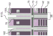
参考图28,漏极选择层级电极条带146通过沉积至少一种导电材料形成于开口85中。举例来说,至少一种导电材料可包含金属屏障层和金属填充材料的组合。金属屏障层包含可充当扩散屏障层和/或用于待随后沉积的金属填充材料的促粘层的导电金属材料。金属屏障层可包含例如TiN、TaN、WN或其堆叠的导电金属氮化物材料。在一个实施例中,金属屏障层可通过例如化学气相沉积(CVD)或原子层沉积(ALD)的保形沉积过程而沉积。金属屏障层的厚度可介于从2nm到8nm的范围内,例如从3nm到6nm,但也可采用更小和更大厚度。在一个实施例中,金属屏障层可基本上由例如TiN等导电金属氮化物组成。金属填充材料可沉积于金属屏障层上以填充横向延伸沟槽87的剩余体积。金属填充材料可通过保形沉积方法沉积,其可为例如化学气相沉积(CVD)、原子层沉积(ALD)、无电镀敷、电镀或其组合。在一个实施例中,金属填充材料可主要由至少一种元素金属组成。金属填充材料层的至少一种元素金属可例如选自钨、钴、钌、钛以及钽。在一个实施例中,金属填充材料层可主要由单种元素金属组成。Referring to FIG. 28, drain selection level electrode strips 146 are formed in openings 85 by depositing at least one conductive material. For example, the at least one conductive material may comprise a combination of a metal barrier layer and a metal fill material. The metal barrier layer comprises a conductive metal material that can act as a diffusion barrier layer and/or an adhesion promoting layer for the metal fill material to be subsequently deposited. The metal barrier layer may comprise conductive metal nitride materials such as TiN, TaN, WN or stacks thereof. In one embodiment, the metal barrier layer may be deposited by a conformal deposition process such as chemical vapor deposition (CVD) or atomic layer deposition (ALD). The thickness of the metal barrier layer may range from 2 nm to 8 nm, eg, from 3 nm to 6 nm, although smaller and larger thicknesses may also be employed. In one embodiment, the metal barrier layer may consist essentially of a conductive metal nitride such as TiN. A metal fill material may be deposited on the metal barrier layer to fill the remaining volume of the laterally extending trenches 87 . The metal fill material can be deposited by conformal deposition methods, which can be, for example, chemical vapor deposition (CVD), atomic layer deposition (ALD), electroless plating, electroplating, or combinations thereof. In one embodiment, the metal filler material may consist essentially of at least one elemental metal. The at least one elemental metal of the metal filling material layer may be selected, for example, from tungsten, cobalt, ruthenium, titanium and tantalum. In one embodiment, the metal fill material layer may consist essentially of a single element metal.

可执行凹部蚀刻以使所述至少一种导电材料凹入,使得所述至少一种导电材料的凹入部分的顶部表面形成于包含漏极区63的顶部表面的水平平面下方。凹入导电材料的每一凹入离散部分构成漏极选择层级电极条带146。漏极选择层级电极条带146形成于从其移除牺牲填充材料层81的体积中。漏极选择层级电极条带146形成于交替堆叠(32、46)上方和相邻对的模板轨道结构77之间,且具有约100nm到约200nm的高度(即,厚度)。A recess etch may be performed to recess the at least one conductive material such that the top surface of the recessed portion of the at least one conductive material is formed below the horizontal plane containing the top surface of the drain region 63 . Each recessed discrete portion of the recessed conductive material constitutes a drain select level electrode strip 146 . Drain select level electrode strips 146 are formed in the volume from which the sacrificial fill material layer 81 is removed. Drain select level electrode strips 146 are formed over the alternating stacks (32, 46) and between adjacent pairs of template track structures 77, and have a height (ie, thickness) of about 100 nm to about 200 nm.

每一漏极选择层级电极条带146接触相应一组圆柱形栅极电极152的外侧壁。每一圆柱形栅极电极152接触漏极选择层级电极条带146中的相应一个。圆柱形栅极电极152包含:第一圆柱形栅极电极152,其在一侧上接触电介质圆柱形片段78'中的相应一个且在另一侧上接触漏极选择层级电极条带146中的相应一个;以及第二圆柱形栅极电极152,其并不接触电介质圆柱形片段78'中的任一个且由漏极选择层级电极条带146中的相应一个横向包围,即环绕。在一个实施例中,圆柱形栅极电极152中的每一个包括掺杂半导体材料,且漏极选择层级电极条带146中的每一个包括至少一种金属材料。所述一对接触的圆柱形栅极电极152和漏极选择层级电极条带146的组合构成漏极选择晶体管的漏极选择栅极电极(146、152)。漏极选择晶体管还包含通道613以及通道613与漏极选择栅极电极(146、152)之间的栅极电介质150。Each drain select level electrode strip 146 contacts the outer sidewalls of a corresponding set of cylindrical gate electrodes 152 . Each cylindrical gate electrode 152 contacts a corresponding one of the drain select level electrode strips 146 . The cylindrical gate electrodes 152 include a first cylindrical gate electrode 152 that contacts a respective one of the dielectric cylindrical segments 78 ′ on one side and contacts a drain select level electrode strip 146 on the other side a respective one; and a second cylindrical gate electrode 152 that does not contact any of the dielectric cylindrical segments 78 ′ and is laterally surrounded, ie, surrounded, by a respective one of the drain select level electrode strips 146 . In one embodiment, each of the cylindrical gate electrodes 152 includes a doped semiconductor material, and each of the drain select level electrode strips 146 includes at least one metallic material. The combination of the pair of contacting cylindrical gate electrodes 152 and drain select level electrode strips 146 constitute the drain select gate electrodes (146, 152) of the drain select transistor. The drain select transistor also includes channel 613 and gate dielectric 150 between channel 613 and the drain select gate electrodes (146, 152).

参见图29,通过例如稀释HF蚀刻的选择性蚀刻移除电介质顶盖275的第一部分275A的剩余部分,以暴露模板轨道结构77的顶部表面。Referring to FIG. 29 , the remainder of the first portion 275A of the dielectric cap 275 is removed by a selective etch, such as a dilute HF etch, to expose the top surface of the template track structure 77 .

参考图30,对漏极选择层级电极条带146、漏极区63、电介质漏极间隔物250、电介质圆柱形片段78'和电介质壁结构76选择性移除暴露模板轨道结构77。在一个实施例中,模板轨道结构77可包含氮化硅,且可采用使用热磷酸的各向同性蚀刻过程来移除模板轨道结构77。横向延伸沟槽87可形成于从其移除模板轨道结构77的体积中。每一横向延伸沟槽87包含大体上沿着第一水平方向hd1延伸的一对侧壁。横向延伸沟槽87的每一侧壁包含所述一对侧壁中的每一个的横向交替序列,包括沿着第一水平方向hd1延伸的笔直侧壁片段和从包含笔直侧壁片段的竖直平面向内横向突出的凸片段。笔直侧壁片段包含相应漏极选择层级电极条带146的平坦竖直侧壁片段。凸片段包含电介质圆柱形片段78'的凸圆柱形侧壁片段。Referring to FIG. 30 , exposed template track structures 77 are selectively removed for drain select level electrode strips 146 , drain regions 63 , dielectric drain spacers 250 , dielectric cylindrical segments 78 ′, and dielectric wall structures 76 . In one embodiment, the template track structures 77 may comprise silicon nitride, and an isotropic etch process using hot phosphoric acid may be employed to remove the template track structures 77 . Laterally extending trenches 87 may be formed in the volume from which template track structures 77 are removed. Each laterally extending trench 87 includes a pair of sidewalls extending generally along the first horizontal direction hd1. Each sidewall of the laterally extending trench 87 comprises a laterally alternating sequence of each of the pair of sidewalls, including straight sidewall segments extending along the first horizontal direction hd1 and vertical sidewall segments comprising straight sidewall segments. A convex segment protruding laterally inward from the plane. The straight sidewall segments include flat vertical sidewall segments of the corresponding drain select level electrode strips 146 . The convex segment comprises the convex cylindrical sidewall segment of the dielectric cylindrical segment 78'.

参考图31A-31C,可在漏极选择层级电极条带146上方通过非保形沉积过程来沉积例如氧化硅或有机硅酸盐玻璃的电介质材料。举例来说,可采用等离子体增强式化学气相沉积(PECVD)来非保形地沉积电介质材料。通过电介质材料的非保形沉积来形成含有轨道形腔89的电介质顶盖层90。电介质顶盖层90形成于横向延伸沟槽87中和漏极选择层级电极条带146上方。电介质顶盖层90包括上覆于漏极选择层级电极条带146的平坦部分以及填充横向延伸沟槽且位于相邻对的漏极选择层级电极条带146之间的向下突出轨道部分。在一个实施例中,向下突出轨道部分中的每一个包括不含任何固相材料或任何液相材料的腔89(即,气隙)。电介质顶盖层90直接形成在电介质圆柱形片段78'的侧壁上。Referring to FIGS. 31A-31C , a dielectric material such as silicon oxide or organosilicate glass may be deposited over the drain select level electrode strips 146 by a non-conformal deposition process. For example, plasma-enhanced chemical vapor deposition (PECVD) may be employed to non-conformally deposit the dielectric material. Dielectric capping layer 90 containing track-shaped cavities 89 is formed by non-conformal deposition of a dielectric material. Dielectric capping layer 90 is formed in laterally extending trenches 87 and over drain select level electrode strips 146 . Dielectric capping layer 90 includes flat portions overlying drain select level electrode strips 146 and downwardly projecting track portions that fill laterally extending trenches and are located between adjacent pairs of drain select level electrode strips 146 . In one embodiment, each of the downwardly projecting track portions includes a cavity 89 (ie, an air gap) that is free of any solid phase material or any liquid phase material. A dielectric capping layer 90 is formed directly on the sidewalls of the dielectric cylindrical segment 78'.

在图31C中所示的一个实施例中,轨道形腔89的竖直横截面形状可包含拱形形状。在一个实施例中,向下突出轨道部分内的每一腔89包含具有随着距衬底8的竖直距离增加而减小的可变宽度的上部部分。在一个实施例中,电介质顶盖层90的向下突出轨道部分中的每一个包含一对侧壁和位于电介质蚀刻终止层73的顶部表面上方的底部部分。由于在电介质顶盖层90的形成期间沉积的电介质材料的几何遮蔽,底部部分的厚度随着距所述一对侧壁中的近侧一个的横向距离增加而增加。在一个实施例中,向下突出轨道部分中的每一个接触沿着第一水平方向hd1布置的两行电介质圆柱形片段78'。In one embodiment shown in Figure 31C, the vertical cross-sectional shape of the track-shaped cavity 89 may comprise an arcuate shape. In one embodiment, each cavity 89 within the downwardly projecting track portion includes an upper portion having a variable width that decreases with increasing vertical distance from the substrate 8 . In one embodiment, each of the downwardly projecting track portions of the dielectric cap layer 90 includes a pair of sidewalls and a bottom portion above the top surface of the dielectric etch stop layer 73 . The thickness of the bottom portion increases with increasing lateral distance from the proximal one of the pair of sidewalls due to geometric shadowing of the dielectric material deposited during the formation of the dielectric capping layer 90 . In one embodiment, each of the downwardly projecting track portions contacts two rows of dielectric cylindrical segments 78' arranged along the first horizontal direction hd1.

如图31B和31C中所示,在上文描述的步骤中的任一个期间,可通过光刻和蚀刻来图案化漏极选择层级电极条带146以移除位于触点区300和外围装置区200中的漏极选择层级电极条带146的部分。可在触点区300和外围装置区200中在从其移除漏极选择层级电极条带146的位置形成平坦化电介质92。电介质顶盖层90可随后形成于位于触点区300和外围装置区200中的平坦化电介质92上方,和位于存储器阵列区100中的漏极选择层级电极条带146上方。As shown in FIGS. 31B and 31C , during any of the steps described above, the drain select level electrode strips 146 may be patterned by photolithography and etching to remove areas located in the contact areas 300 and peripheral devices The drain in 200 selects the portion of the level electrode strip 146 . Planarized dielectric 92 may be formed in contact region 300 and peripheral device region 200 at locations from which drain select level electrode strips 146 were removed. Dielectric capping layer 90 may then be formed over planarized dielectric 92 in contact region 300 and peripheral device region 200 , and over drain select level electrode strips 146 in memory array region 100 .

栅极触点通孔结构86穿过电介质顶盖层90、平坦化电介质92和逆向阶梯式电介质65中的开口与相应导电层(例如,字线)46或漏极选择层级电极条带146接触而形成。漏极触点通孔结构88穿过电介质顶盖层90中的开口形成以接触漏极区63。位线(未示出)随后与漏极触点通孔结构88电接触而形成。Gate contact via structures 86 contact corresponding conductive layers (eg, word lines) 46 or drain select level electrode strips 146 through openings in dielectric cap layer 90 , planarization dielectric 92 , and reverse stepped dielectric 65 formed. Drain contact via structures 88 are formed through openings in dielectric cap layer 90 to contact drain regions 63 . A bit line (not shown) is then formed in electrical contact with the drain contact via structure 88 .

参考本公开的所有附图,提供三维存储器装置,其包括位于衬底8上方的绝缘层32和字线46的交替堆叠,延伸穿过交替堆叠(32、46)且包括相应竖直半导体通道611和相应存储器膜50的存储器堆叠结构55,位于交替堆叠上方、沿着第一水平方向延伸且沿着第二水平方向横向隔开的漏极选择栅极电极(146、152),以及位于邻近漏极选择栅极电极之间的电介质顶盖层90。气隙89在邻近漏极选择栅极电极之间位于电介质顶盖层90中。Referring to all figures of the present disclosure, a three-dimensional memory device is provided that includes alternating stacks of insulating layers 32 and word lines 46 over a substrate 8, extending through the alternating stacks (32, 46) and including respective vertical semiconductor channels 611 and memory stack structure 55 of corresponding memory films 50, over alternate stacks, drain select gate electrodes (146, 152) extending along the first horizontal direction and laterally spaced along the second horizontal direction, and adjacent to the drain Dielectric capping layer 90 between the pole select gate electrodes. Air gaps 89 are located in dielectric cap layer 90 between adjacent drain select gate electrodes.

在一个实施例中,漏极选择层级柱结构158位于存储器堆叠结构55中的相应一个上,其中漏极选择层级柱结构158中的每一个包括接触存储器堆叠结构55中的下伏存储器堆叠结构的漏极选择层级通道613。In one embodiment, the drain select level pillar structures 158 are located on respective ones of the memory stack structures 55 , wherein each of the drain select level pillar structures 158 includes a contact point of an underlying memory stack structure in the memory stack structures 55 . Drain select level channel 613 .

在一个实施例中,电介质顶盖层90包括上覆于漏极选择栅极电极(146、152)的平坦部分(例如,漏极选择层级电极条带146)和位于相邻对的漏极选择栅极电极之间的向下突出轨道部分。向下突出轨道部分中的每一个包括气隙89,其为不含任何固相材料或任何液相材料的腔。In one embodiment, dielectric capping layer 90 includes a flat portion (eg, drain select level electrode strip 146) overlying the drain select gate electrodes (146, 152) and a drain select in an adjacent pair The downwardly protruding track portion between the gate electrodes. Each of the downwardly projecting track portions includes an air gap 89, which is a cavity free of any solid phase material or any liquid phase material.

在一个实施例中,向下突出轨道部分内的每一腔(即,气隙89)是大体上沿着第一水平方向hd1延伸且具有沿着第二水平方向hd2的橫向起伏的横向起伏的腔。在一个实施例中,向下突出轨道部分内的每一腔包含具有随着距衬底8的竖直距离增加而减小的可变宽度的上部部分。In one embodiment, each cavity (ie, air gap 89 ) within the downwardly projecting track portion is laterally undulating extending generally along the first horizontal direction hd1 and having lateral undulations along the second horizontal direction hd2 cavity. In one embodiment, each cavity within the downwardly projecting track portion includes an upper portion having a variable width that decreases with increasing vertical distance from the substrate 8 .

在一个实施例中,其中每一漏极选择栅极电极(146、152)包括接触相应漏极选择层级电极条带146的相应圆柱形栅极电极152。因此,每一圆柱形栅极电极152包括相应漏极选择栅极电极的一部分和相应漏极选择层级柱结构158的一部分。In one embodiment, wherein each drain select gate electrode ( 146 , 152 ) includes a respective cylindrical gate electrode 152 that contacts a respective drain select level electrode strip 146 . Thus, each cylindrical gate electrode 152 includes a portion of a corresponding drain select gate electrode and a portion of a corresponding drain select level pillar structure 158 .

示例性结构可包含三维存储器装置。在一个实施例中,三维存储器装置包括单片三维NAND存储器装置。衬底8可包括硅衬底。竖直NAND存储器装置可包括在硅衬底上方的单片三维NAND串阵列。单片三维NAND串阵列的第一装置层级中的至少一个存储器单元(如体现为字线层级导电层46的层级处的电荷存储层54的一部分)可位于单片三维NAND串阵列的第二装置层级中的另一存储器单元(如体现为另一字线层级导电层46的层级处的电荷存储层54的另一部分)上方。硅衬底可包含集成电路,所述集成电路包括用于位于其上的存储器装置的驱动器电路(如体现为至少一个半导体装置700的子组)。字线层级导电层46可包括具有基本上平行于衬底8的顶部表面,例如在一对背侧沟槽79之间延伸的条带形状的多个控制栅极电极。所述多个控制栅极电极包括位于第一装置层级中的至少第一控制栅极电极,和位于第二装置层级中的第二控制栅极电极。单片三维NAND串的阵列可包括:多个半导体通道(611、613),其中所述多个半导体通道(611、613)中的每一个的至少一个末端部分基本上垂直于衬底8的顶部表面延伸且包括竖直半导体通道611中的相应一个;以及多个电荷存储元件(体现为存储器膜50的部分,即,电荷存储层54的部分)。每一电荷存储元件可邻近于所述多个半导体通道(611)中的相应一个定位。Exemplary structures may include three-dimensional memory devices. In one embodiment, the three-dimensional memory device comprises a monolithic three-dimensional NAND memory device. The substrate 8 may comprise a silicon substrate. A vertical NAND memory device may include a monolithic three-dimensional array of NAND strings over a silicon substrate. At least one memory cell in a first device level of the monolithic three-dimensional NAND string array, such as a portion of charge storage layer 54 at the level embodied as word line level conductive layer 46, may be located in a second device of the monolithic three-dimensional NAND string array Above another memory cell in a level, such as another portion of charge storage layer 54 at a level embodied as another word line level conductive layer 46 . The silicon substrate may contain integrated circuits including driver circuits for memory devices located thereon (eg, embodied as a subset of at least one semiconductor device 700). The wordline level conductive layer 46 may include a plurality of control gate electrodes having a stripe shape substantially parallel to the top surface of the substrate 8 , eg, extending between a pair of backside trenches 79 . The plurality of control gate electrodes includes at least a first control gate electrode in a first device level, and a second control gate electrode in a second device level. The array of monolithic three-dimensional NAND strings may include a plurality of semiconductor channels ( 611 , 613 ), wherein at least one end portion of each of the plurality of semiconductor channels ( 611 , 613 ) is substantially perpendicular to the top of the substrate 8 The surface extends and includes a respective one of the vertical semiconductor channels 611; and a plurality of charge storage elements (embodied as part of memory film 50, ie, part of charge storage layer 54). Each charge storage element may be positioned adjacent to a respective one of the plurality of semiconductor channels (611).

电介质顶盖层90的向下突出轨道部分内的气隙89具有约1.0的介电常数,且因此,减少相邻对的漏极选择层级电极条带146之间的电容性耦合。此外,电介质顶盖层90的向下突出轨道部分自对准于漏极选择层级柱结构158。因此,漏极选择层级柱结构158的在间距上的阵列可与存储器堆叠结构55的下伏在间距上的阵列结合使用,以提供竖直NAND串的紧凑周期性二维阵列。The air gap 89 within the downwardly protruding track portion of the dielectric cap layer 90 has a dielectric constant of about 1.0, and thus, reduces capacitive coupling between adjacent pairs of drain select level electrode strips 146 . Additionally, the downward protruding track portion of the dielectric cap layer 90 is self-aligned with the drain select level pillar structure 158 . Accordingly, the on-pitch array of drain select level pillar structures 158 can be used in conjunction with the underlying on-pitch array of memory stack structures 55 to provide a compact periodic two-dimensional array of vertical NAND strings.

虽然前述内容是指特定的优选实施例,但应了解,本公开限于此。所属领域的一般技术人员将想到可对所公开的实施例作各种修改且此类修改意图在本公开的范围内。假定并非彼此的替代方案的所有实施例当中存在兼容性。除非另外明确地陈述,否则字词“包括”或“包含”涵盖其中字词“基本上由…组成”或字词“由…组成”代替字词“包括”或“包含”的所有实施例。在本公开中说明采用特定结构和/或配置的实施例的情况下,应理解,可以用在功能上等效的任何其它相容结构和/或配置实践本公开,条件是此类替代物并未被明确禁用或以其它方式被所属领域的技术人员认为是不可能的。所有本文中列举的公开、专利申请和专利以全文引用的方式并入本文中。While the foregoing is directed to specific preferred embodiments, it should be understood that the present disclosure is limited thereto. Various modifications to the disclosed embodiments will occur to those of ordinary skill in the art and such modifications are intended to be within the scope of the present disclosure. Compatibility is assumed among all embodiments that are not alternatives to each other. Unless expressly stated otherwise, the word "comprising" or "comprising" encompasses all embodiments in which the word "consisting essentially of" or the word "consisting of" replaces the word "comprising" or "comprising". Where embodiments employing particular structures and/or configurations are described in this disclosure, it should be understood that the present disclosure may be practiced with any other compatible structures and/or configurations that are functionally equivalent, provided that such alternatives do not Not expressly disabled or otherwise considered impossible by those skilled in the art. All publications, patent applications and patents listed herein are incorporated by reference in their entirety.

Claims (20)

1. A three-dimensional memory device, comprising:
an alternating stack of insulating layers and word lines over a substrate;
memory stack structures extending through the alternating stack and comprising respective vertical semiconductor channels and respective memory films;
a drain select gate electrode over the alternating stack, extending along a first horizontal direction, and laterally spaced along a second horizontal direction; and
a dielectric cap layer located between adjacent drain select gate electrodes, wherein an air gap is located in the dielectric cap layer between adjacent drain select gate electrodes.
2. The three-dimensional memory device of claim 1, further comprising drain select level pillar structures located on a respective one of the memory stack structures, wherein each of the drain select level pillar structures comprises a drain select level channel that contacts an underlying one of the memory stack structures.
3. The three-dimensional memory device of claim 2, wherein:
the dielectric cap layer includes a planar portion overlying the drain select gate electrode and a downwardly projecting rail portion between adjacent pairs of the drain select gate electrodes; and is
Each of the downwardly projecting track portions includes the air gap, which is a cavity that is free of any solid phase material or any liquid phase material.
4. The three-dimensional memory device of claim 3, wherein each cavity within the downwardly projecting rail portion is a laterally undulating cavity extending generally along the first horizontal direction and having a laterally undulation along the second horizontal direction.
5. The three-dimensional memory device of claim 4, wherein each cavity within the downwardly protruding rail portion includes an upper portion having a variable width that decreases with increasing vertical distance from the substrate.
6. The three-dimensional memory device of claim 3, wherein each of the drain select level pillar structures comprises:
a cylindrical gate dielectric laterally surrounding the drain select level channel; and
a cylindrical gate electrode laterally surrounding the cylindrical gate dielectric.
7. The three-dimensional memory device of claim 6, wherein each drain select gate electrode comprises a respective cylindrical gate electrode that contacts a respective drain select level electrode strip.
8. The three-dimensional memory device of claim 7, wherein each of the downwardly projecting rail portions contacts two rows of dielectric cylindrical segments arranged along the first horizontal direction.
9. The three-dimensional memory device of claim 8, wherein the cylindrical gate electrode comprises:
first cylindrical gate electrodes contacting, on one side, respective ones of the dielectric cylindrical segments and contacting respective drain select level electrode strips; and
a second cylindrical gate electrode that does not contact any of the dielectric cylindrical segments and is laterally surrounded by the drain select level electrode strip.
10. The three-dimensional memory device of claim 7, wherein:
each of the cylindrical gate electrodes comprises a doped semiconductor material; and is
Each of the drain select level electrode strips comprises a metal material.
11. The three-dimensional memory device of claim 2, wherein:
the three-dimensional memory device comprises a monolithic three-dimensional NAND memory device;
the drain select level pillar structures are arranged in rows extending along the first horizontal direction; and is
The row-to-row spacing is the same for each adjacent pair of rows of the drain select level pillar structures.
12. The three-dimensional memory device of claim 11, wherein:
the drain select level pillar structures are arranged in a first two-dimensional hexagonal array; and is
The memory stack structures are arranged in a second two-dimensional hexagonal array having the same two-dimensional periodicity as the first two-dimensional hexagonal array.
13. The three-dimensional memory device of claim 7, further comprising a dielectric etch stop layer between the alternating stacks and the drain select level electrode strips, wherein each drain select level channel extends through a respective opening through the dielectric etch stop layer.
14. The three-dimensional memory device of claim 13, wherein each of the downwardly projecting rail portions of the dielectric cap layer includes a pair of sidewalls and a bottom portion that contacts a top surface of the dielectric etch stop layer, wherein a thickness of the bottom portion increases with increasing lateral distance from a proximal one of the pair of sidewalls.
15. A method of forming a three-dimensional memory device, comprising:
forming an alternating stack of insulating layers and spacer material layers over a substrate, wherein the spacer material layers are formed as or replaced by wordline-level conductive layers;
forming memory stack structures through the alternating stack, wherein each of the memory stack structures includes a respective vertical semiconductor channel and a respective memory film;
forming a template rail structure over the alternating stack;
forming drain select level pillar structures over the memory stack structures, wherein each of the drain select level pillar structures comprises a drain select level channel that contacts an underlying one of the memory stack structures;
forming drain select level electrode strips over the alternating stacks and between adjacent pairs of the template rail structures;
forming laterally extending trenches by removing the template rail structure; and
forming a dielectric cap layer in the laterally extending trenches and over the drain select level electrode strips, wherein the dielectric cap layer comprises a planar portion overlying the drain select level electrode strips and downwardly projecting rail portions filling the laterally extending trenches and located between adjacent pairs of the drain select level electrode strips, wherein each of the downwardly projecting rail portions comprises a cavity free of any solid phase material or any liquid phase material.
16. The method of claim 15, wherein:
the formwork track structure extends along a first horizontal direction and is laterally spaced along a second horizontal direction; and is
Each sidewall of the template rail structure extending along the first horizontal direction is perforated by a respective row of drain select level pillar structures.
17. The method of claim 16, wherein:
each of the laterally extending trenches includes a pair of sidewalls extending generally along the first horizontal direction; and is
Each of the pair of sidewalls includes a straight sidewall segment extending along the first horizontal direction and a convex segment projecting laterally inward from a vertical plane containing the straight sidewall segment.
18. The method of claim 15, wherein each cavity within the downwardly projecting rail portion includes an upper portion having a variable width that decreases with increasing vertical distance from the substrate.
19. The method of claim 15, further comprising:
forming a layer of sacrificial fill material over the alternating stack; and
forming drain select level openings through the layer of sacrificial fill material and the template rail structures, wherein a first subset of the drain select level openings extend through a respective one of the template rail structures and a portion of the layer of sacrificial fill material, and a second subset of the drain select level openings are laterally spaced from the template rail structures,
wherein the drain select level pillar structures are formed within respective ones of the drain select level openings.
20. The method of claim 19, wherein each of the drain select level pillar structures comprises:
a cylindrical gate dielectric laterally surrounding a respective one of the drain select level channels; and
a cylindrical gate electrode laterally surrounding the cylindrical gate dielectric.
CN201980006271.9A 2018-08-20 2019-05-14 Three-dimensional memory device containing drain-selective level air gap and method of manufacturing same Active CN111448662B (en)

Applications Claiming Priority (5)

Application Number Priority Date Filing Date Title
US201862719893P 2018-08-20 2018-08-20
US62/719,893 2018-08-20
US16/136,686 US10741576B2 (en) 2018-08-20 2018-09-20 Three-dimensional memory device containing drain-select-level air gap and methods of making the same
US16/136,686 2018-09-20
PCT/US2019/032174 WO2020040833A1 (en) 2018-08-20 2019-05-14 Three-dimensional memory device containing drain-selct-level air gap and methods of making the same

Publications (2)

Publication Number Publication Date
CN111448662A true CN111448662A (en) 2020-07-24
CN111448662B CN111448662B (en) 2023-10-31

Family

ID=69523415

Family Applications (1)

Application Number Title Priority Date Filing Date
CN201980006271.9A Active CN111448662B (en) 2018-08-20 2019-05-14 Three-dimensional memory device containing drain-selective level air gap and method of manufacturing same

Country Status (3)

Country Link
US (1) US10741576B2 (en)
CN (1) CN111448662B (en)
WO (1) WO2020040833A1 (en)

Cited By (5)

* Cited by examiner, † Cited by third party
Publication number Priority date Publication date Assignee Title
CN113270421A (en) * 2021-05-17 2021-08-17 长江存储科技有限责任公司 Three-dimensional memory and preparation method thereof
CN114664855A (en) * 2022-03-14 2022-06-24 长江存储科技有限责任公司 Semiconductor structure, preparation method thereof, three-dimensional memory and storage system
CN115440672A (en) * 2022-08-18 2022-12-06 长江存储科技有限责任公司 Three-dimensional memory, its manufacturing method and storage system
WO2023108330A1 (en) * 2021-12-13 2023-06-22 Yangtze Memory Technologies Co., Ltd. Three-dimensional memory device with divided drain select gate lines and method for forming the same
CN117241587A (en) * 2022-06-15 2023-12-15 美光科技公司 Electronic devices including source seals and related methods and electronic systems

Families Citing this family (40)

* Cited by examiner, † Cited by third party
Publication number Priority date Publication date Assignee Title
US11552094B2 (en) 2017-07-18 2023-01-10 Sandisk Technologies Llc Three-dimensional memory device having on-pitch drain select gate electrodes and method of making the same
US11037943B2 (en) * 2017-07-18 2021-06-15 Sandisk Technologies Llc Three-dimensional memory device having on-pitch drain select gate electrodes and method of making the same
US10756105B2 (en) * 2018-11-26 2020-08-25 Micron Technology, Inc. Memory arrays and methods used in forming a memory array
JP7270740B2 (en) * 2018-12-20 2023-05-10 アプライド マテリアルズ インコーポレイテッド Fabrication of memory cells for 3D NAND applications
US10937800B2 (en) 2019-03-13 2021-03-02 Sandisk Technologies Llc Three-dimensional memory device with on-axis self-aligned drain-select-level isolation structure and methods of manufacturing the same
CN110914986B (en) 2019-03-29 2021-05-14 长江存储科技有限责任公司 Three-dimensional memory device and manufacturing method thereof
WO2020199388A1 (en) 2019-03-29 2020-10-08 Yangtze Memory Technologies Co., Ltd. Three-dimensional memory devices and fabrication methods thereof
CN110896672B (en) * 2019-03-29 2021-05-25 长江存储科技有限责任公司 Three-dimensional memory device and manufacturing method thereof
CN110896671B (en) 2019-03-29 2021-07-30 长江存储科技有限责任公司 Three-dimensional memory device and manufacturing method thereof
CN110896670B (en) 2019-03-29 2021-06-08 长江存储科技有限责任公司 Three-dimensional memory device and manufacturing method thereof
US11075219B2 (en) 2019-08-20 2021-07-27 Micron Technology, Inc. Memory arrays and methods used in forming a memory array comprising strings of memory cells
US11195848B2 (en) 2019-08-25 2021-12-07 Micron Technology, Inc. Memory arrays and methods used in forming a memory array comprising strings of memory cells
US11563022B2 (en) 2019-08-25 2023-01-24 Micron Technology, Inc. Memory arrays and methods used in forming a memory array comprising strings of memory cells
US11195850B2 (en) 2019-10-18 2021-12-07 Micron Technology, Inc. Memory arrays and methods used in forming a memory array comprising strings of memory cells
US11101210B2 (en) 2019-10-25 2021-08-24 Micron Technology, Inc. Methods for manufacturing a memory array having strings of memory cells comprising forming bridge material between memory blocks
KR102849979B1 (en) * 2020-03-16 2025-08-27 삼성전자주식회사 Semiconductor devices having a stud connected to string selection line
US11222954B2 (en) 2020-03-24 2022-01-11 Sandisk Technologies Llc Three-dimensional memory device containing inter-select-gate electrodes and methods of making the same
US11398496B2 (en) * 2020-04-27 2022-07-26 Sandisk Technologies Llc Three-dimensional memory device employing thinned insulating layers and methods for forming the same
WO2021221738A1 (en) * 2020-04-27 2021-11-04 Sandisk Technologies Llc Three-dimensional memory device employing thinned insulating layers and methods for forming the same
US11489043B2 (en) 2020-04-27 2022-11-01 Sandisk Technologies Llc Three-dimensional memory device employing thinned insulating layers and methods for forming the same
US11152284B1 (en) 2020-05-07 2021-10-19 Sandisk Technologies Llc Three-dimensional memory device with a dielectric isolation spacer and methods of forming the same
US11985825B2 (en) 2020-06-25 2024-05-14 Taiwan Semiconductor Manufacturing Co., Ltd. 3D memory array contact structures
KR102812031B1 (en) * 2020-06-25 2025-05-26 삼성전자주식회사 Semiconductor device
US11653500B2 (en) 2020-06-25 2023-05-16 Taiwan Semiconductor Manufacturing Co., Ltd. Memory array contact structures
US11532343B2 (en) 2020-06-26 2022-12-20 Taiwan Semiconductor Manufacturing Co., Ltd. Memory array including dummy regions
US11600520B2 (en) 2020-06-26 2023-03-07 Taiwan Semiconductor Manufacturing Co., Ltd. Air gaps in memory array structures
US11640974B2 (en) 2020-06-30 2023-05-02 Taiwan Semiconductor Manufacturing Co., Ltd. Memory array isolation structures
US11889683B2 (en) * 2020-07-01 2024-01-30 Micron Technology, Inc. Memory arrays comprising strings of memory cells and methods used in forming a memory array comprising strings of memory cells
US11647634B2 (en) 2020-07-16 2023-05-09 Taiwan Semiconductor Manufacturing Co., Ltd. Three-dimensional memory device and method
US11355516B2 (en) 2020-07-16 2022-06-07 Taiwan Semiconductor Manufacturing Co., Ltd. Three-dimensional memory device and method
US11495618B2 (en) 2020-07-30 2022-11-08 Taiwan Semiconductor Manufacturing Co., Ltd. Three-dimensional memory device and method
US11605589B2 (en) * 2021-01-28 2023-03-14 Micron Technology, Inc. Methods of forming microelectronic devices, and related microelectronic devices, memory devices, and electronic systems
US11716856B2 (en) 2021-03-05 2023-08-01 Taiwan Semiconductor Manufacturing Co., Ltd. Three-dimensional memory device and method
US12211746B2 (en) * 2021-04-15 2025-01-28 Micron Technology, Inc. Methods used in forming a memory array comprising strings of memory cells including forming a pair of elevationally-extending walls that are laterally-spaced relative one another and that are individually horizontally-longitudinally-elongated
US12004347B2 (en) 2021-04-22 2024-06-04 Sandisk Technologies Llc Three-dimensional memory device including self-aligned drain-select-level isolation structures and method of making thereof
US11871580B2 (en) 2021-05-11 2024-01-09 Sandisk Technologies Llc Three-dimensional memory device including low-k drain-select-level isolation structures and methods of forming the same
US11856765B2 (en) 2021-05-11 2023-12-26 Sandisk Technologies Llc Three-dimensional memory device including low-k drain-select-level isolation structures and methods of forming the same
US11756596B1 (en) * 2022-05-24 2023-09-12 Micron Technology, Inc. Transition structures for three-dimensional memory arrays
US12476192B2 (en) * 2022-07-26 2025-11-18 SanDisk Technologies, Inc. Three-dimensional memory device including a drain contact etch-stop dielectric layer and methods for forming the same
JP2025539159A (en) * 2022-12-02 2025-12-03 アプライド マテリアルズ インコーポレイテッド Formation of word line contacts for NAND devices

Citations (5)

* Cited by examiner, † Cited by third party
Publication number Priority date Publication date Assignee Title
US20150008503A1 (en) * 2013-07-02 2015-01-08 SanDisk Technologies, Inc. Method Of Making A Three-Dimensional Memory Array With Etch Stop
US20150069496A1 (en) * 2013-09-10 2015-03-12 Kabushiki Kaisha Toshiba Semiconductor storage device
US20160111435A1 (en) * 2014-10-15 2016-04-21 Sandisk Technologies Inc. Three-dimensional memory structure having self-aligned drain regions and methods of making thereof
US9419012B1 (en) * 2015-06-19 2016-08-16 Sandisk Technologies Llc Three-dimensional memory structure employing air gap isolation
US20180211970A1 (en) * 2016-11-17 2018-07-26 Sandisk Technologies Llc Three-dimensional memory device with self-aligned drain side select gate electrodes and method of making thereof

Family Cites Families (23)

* Cited by examiner, † Cited by third party
Publication number Priority date Publication date Assignee Title
US5915167A (en) 1997-04-04 1999-06-22 Elm Technology Corporation Three dimensional structure memory
US9397093B2 (en) 2013-02-08 2016-07-19 Sandisk Technologies Inc. Three dimensional NAND device with semiconductor, metal or silicide floating gates and method of making thereof
US8349681B2 (en) 2010-06-30 2013-01-08 Sandisk Technologies Inc. Ultrahigh density monolithic, three dimensional vertical NAND memory device
KR20130044711A (en) 2011-10-24 2013-05-03 에스케이하이닉스 주식회사 Three dimension non-volatile memory device, memory system comprising the same and method of manufacturing the same
US8847302B2 (en) 2012-04-10 2014-09-30 Sandisk Technologies Inc. Vertical NAND device with low capacitance and silicided word lines
US8658499B2 (en) 2012-07-09 2014-02-25 Sandisk Technologies Inc. Three dimensional NAND device and method of charge trap layer separation and floating gate formation in the NAND device
US9449982B2 (en) 2013-03-12 2016-09-20 Sandisk Technologies Llc Method of making a vertical NAND device using a sacrificial layer with air gap and sequential etching of multilayer stacks
US9252151B2 (en) 2013-07-08 2016-02-02 Sandisk Technologies Inc. Three dimensional NAND device with birds beak containing floating gates and method of making thereof
US9356031B2 (en) 2014-08-11 2016-05-31 Sandisk Technologies Inc. Three dimensional NAND string memory devices with voids enclosed between control gate electrodes
US9576975B2 (en) 2014-08-26 2017-02-21 Sandisk Technologies Llc Monolithic three-dimensional NAND strings and methods of fabrication thereof
US9691884B2 (en) 2014-08-26 2017-06-27 Sandisk Technologies Llc Monolithic three dimensional NAND strings and methods of fabrication thereof
US9515085B2 (en) 2014-09-26 2016-12-06 Sandisk Technologies Llc Vertical memory device with bit line air gap
US9484250B2 (en) * 2015-03-10 2016-11-01 International Business Machines Corporation Air gap contact formation for reducing parasitic capacitance
US9627399B2 (en) 2015-07-24 2017-04-18 Sandisk Technologies Llc Three-dimensional memory device with metal and silicide control gates
US9646975B2 (en) 2015-09-21 2017-05-09 Sandisk Technologies Llc Lateral stack of cobalt and a cobalt-semiconductor alloy for control gate electrodes in a memory structure
US9842907B2 (en) 2015-09-29 2017-12-12 Sandisk Technologies Llc Memory device containing cobalt silicide control gate electrodes and method of making thereof
KR102432776B1 (en) 2015-10-08 2022-08-17 에스케이하이닉스 주식회사 Manufacturing method of semiconductor device
US9793139B2 (en) 2015-10-29 2017-10-17 Sandisk Technologies Llc Robust nucleation layers for enhanced fluorine protection and stress reduction in 3D NAND word lines
US10115732B2 (en) 2016-02-22 2018-10-30 Sandisk Technologies Llc Three dimensional memory device containing discrete silicon nitride charge storage regions
KR102607838B1 (en) 2016-06-01 2023-11-30 에스케이하이닉스 주식회사 Semiconductor device and manufacturing method thereof
US9666533B1 (en) * 2016-06-30 2017-05-30 International Business Machines Corporation Airgap formation between source/drain contacts and gates
US10050054B2 (en) 2016-10-05 2018-08-14 Sandisk Technologies Llc Three-dimensional memory device having drain select level isolation structure and method of making thereof
US9875929B1 (en) 2017-01-23 2018-01-23 Sandisk Technologies Llc Three-dimensional memory device with annular blocking dielectrics and discrete charge storage elements and method of making thereof

Patent Citations (5)

* Cited by examiner, † Cited by third party
Publication number Priority date Publication date Assignee Title
US20150008503A1 (en) * 2013-07-02 2015-01-08 SanDisk Technologies, Inc. Method Of Making A Three-Dimensional Memory Array With Etch Stop
US20150069496A1 (en) * 2013-09-10 2015-03-12 Kabushiki Kaisha Toshiba Semiconductor storage device
US20160111435A1 (en) * 2014-10-15 2016-04-21 Sandisk Technologies Inc. Three-dimensional memory structure having self-aligned drain regions and methods of making thereof
US9419012B1 (en) * 2015-06-19 2016-08-16 Sandisk Technologies Llc Three-dimensional memory structure employing air gap isolation
US20180211970A1 (en) * 2016-11-17 2018-07-26 Sandisk Technologies Llc Three-dimensional memory device with self-aligned drain side select gate electrodes and method of making thereof

Cited By (7)

* Cited by examiner, † Cited by third party
Publication number Priority date Publication date Assignee Title
CN113270421A (en) * 2021-05-17 2021-08-17 长江存储科技有限责任公司 Three-dimensional memory and preparation method thereof
US12266403B2 (en) 2021-05-17 2025-04-01 Yangtze Memory Technologies Co., Ltd. Three-dimensional NAND memory and fabrication method thereof
WO2023108330A1 (en) * 2021-12-13 2023-06-22 Yangtze Memory Technologies Co., Ltd. Three-dimensional memory device with divided drain select gate lines and method for forming the same
US12302560B2 (en) 2021-12-13 2025-05-13 Yangtze Memory Technologies Co., Ltd. Three-dimensional memory device with divided drain select gate lines and method for forming the same
CN114664855A (en) * 2022-03-14 2022-06-24 长江存储科技有限责任公司 Semiconductor structure, preparation method thereof, three-dimensional memory and storage system
CN117241587A (en) * 2022-06-15 2023-12-15 美光科技公司 Electronic devices including source seals and related methods and electronic systems
CN115440672A (en) * 2022-08-18 2022-12-06 长江存储科技有限责任公司 Three-dimensional memory, its manufacturing method and storage system

Also Published As

Publication number Publication date
US10741576B2 (en) 2020-08-11
US20200058673A1 (en) 2020-02-20
CN111448662B (en) 2023-10-31
WO2020040833A1 (en) 2020-02-27

Similar Documents

Publication Publication Date Title
CN111448662B (en) Three-dimensional memory device containing drain-selective level air gap and method of manufacturing same
US11621277B2 (en) Multilevel memory stack structure with tapered inter-tier joint region and methods of making thereof
KR102342709B1 (en) Three-dimensional memory device and its manufacturing methods using alternative drain select gate electrodes
CN111418064B (en) Three-Dimensional Inverse Planar NAND Memory Device Comprising Partially Discrete Charge Storage Elements and Method of Fabrication
US11469241B2 (en) Three-dimensional memory device including discrete charge storage elements and methods of forming the same
CN111512442B (en) Three-dimensional flat NAND memory device including wavy word lines and method of fabricating the same
CN110832643B (en) Three-dimensional memory device with self-aligned multi-level drain select gate electrodes and method of manufacturing the same
US10553599B1 (en) Three-dimensional memory device containing drain select isolation structures and on-pitch channels and methods of making the same without an etch stop layer
US10290650B1 (en) Self-aligned tubular electrode portions inside memory openings for drain select gate electrodes in a three-dimensional memory device
CN114946027B (en) A three-dimensional memory device including a back-side trench support structure and a method for forming the same.
CN109791931B (en) Three-dimensional memory device with non-uniform spacing between memory stack structures and method of manufacturing the same
US10868025B2 (en) Three-dimensional memory device including replacement crystalline channels and methods of making the same
EP3494596B1 (en) Three-dimensional memory device with self-aligned drain side select gate electrodes and method of making thereof
US11387244B2 (en) Three-dimensional memory device including discrete charge storage elements and methods of forming the same
EP3375014B1 (en) Three dimensional memory device with peripheral devices under dummy dielectric layer stack and method of making thereof
CN108012567B (en) Lateral stacks of cobalt and cobalt-semiconductor alloys for control gate electrodes in memory structures
CN108140644B (en) Replacement openings in arrays for three-dimensional memory devices
US9859363B2 (en) Self-aligned isolation dielectric structures for a three-dimensional memory device
CN111373534B (en) Three-dimensional memory device including multi-level drain select gate isolation and method of manufacturing the same
CN111512441B (en) Three-dimensional memory device including a bottle-shaped memory stack structure and method of manufacturing the same
CN111448661A (en) Three-dimensional planar memory device including a double-dipole blocking dielectric layer and method of making the same
CN111433912A (en) Three-dimensional memory device containing source contact to vertical channel bottom and method of making the same
US10756106B2 (en) Three-dimensional memory device with locally modulated threshold voltages at drain select levels and methods of making the same
KR102799458B1 (en) Semiconductor device including bit lines separated by air gaps and method for forming the same
CN116724675A (en) Lateral transistors for selecting blocks in three-dimensional memory arrays and methods of forming the same

Legal Events

Date Code Title Description
PB01 Publication
PB01 Publication
SE01 Entry into force of request for substantive examination
GR01 Patent grant
GR01 Patent grant
TR01 Transfer of patent right

Effective date of registration: 20250319

Address after: U.S.A.

Patentee after: SANDISK TECHNOLOGIES Inc.

Country or region after: U.S.A.

Address before: texas

Patentee before: SANDISK TECHNOLOGIES LLC

Country or region before: U.S.A.