CN111370943A - Electrical connector - Google Patents
Electrical connector Download PDFInfo
- Publication number
- CN111370943A CN111370943A CN202010155226.4A CN202010155226A CN111370943A CN 111370943 A CN111370943 A CN 111370943A CN 202010155226 A CN202010155226 A CN 202010155226A CN 111370943 A CN111370943 A CN 111370943A
- Authority
- CN
- China
- Prior art keywords
- electrical connector
- terminal
- signal terminal
- groove
- contact
- Prior art date
- Legal status (The legal status is an assumption and is not a legal conclusion. Google has not performed a legal analysis and makes no representation as to the accuracy of the status listed.)
- Pending
Links
- 239000002184 metal Substances 0.000 claims abstract description 22
- 230000013011 mating Effects 0.000 claims description 13
- 239000007769 metal material Substances 0.000 claims description 3
- 230000000149 penetrating effect Effects 0.000 claims description 2
- 238000009413 insulation Methods 0.000 claims 1
- 230000008054 signal transmission Effects 0.000 abstract description 3
- 238000009434 installation Methods 0.000 description 18
- 230000000694 effects Effects 0.000 description 7
- 230000008878 coupling Effects 0.000 description 3
- 238000010168 coupling process Methods 0.000 description 3
- 238000005859 coupling reaction Methods 0.000 description 3
- 238000003032 molecular docking Methods 0.000 description 3
- 230000005540 biological transmission Effects 0.000 description 2
- 230000005489 elastic deformation Effects 0.000 description 2
- 238000006243 chemical reaction Methods 0.000 description 1
- 238000009713 electroplating Methods 0.000 description 1
- 239000000463 material Substances 0.000 description 1
- 238000000034 method Methods 0.000 description 1
- 238000005476 soldering Methods 0.000 description 1
Images


Classifications
-
- H—ELECTRICITY
- H01—ELECTRIC ELEMENTS
- H01R—ELECTRICALLY-CONDUCTIVE CONNECTIONS; STRUCTURAL ASSOCIATIONS OF A PLURALITY OF MUTUALLY-INSULATED ELECTRICAL CONNECTING ELEMENTS; COUPLING DEVICES; CURRENT COLLECTORS
- H01R13/00—Details of coupling devices of the kinds covered by groups H01R12/70 or H01R24/00 - H01R33/00
- H01R13/648—Protective earth or shield arrangements on coupling devices, e.g. anti-static shielding
-
- H—ELECTRICITY
- H01—ELECTRIC ELEMENTS
- H01R—ELECTRICALLY-CONDUCTIVE CONNECTIONS; STRUCTURAL ASSOCIATIONS OF A PLURALITY OF MUTUALLY-INSULATED ELECTRICAL CONNECTING ELEMENTS; COUPLING DEVICES; CURRENT COLLECTORS
- H01R12/00—Structural associations of a plurality of mutually-insulated electrical connecting elements, specially adapted for printed circuits, e.g. printed circuit boards [PCB], flat or ribbon cables, or like generally planar structures, e.g. terminal strips, terminal blocks; Coupling devices specially adapted for printed circuits, flat or ribbon cables, or like generally planar structures; Terminals specially adapted for contact with, or insertion into, printed circuits, flat or ribbon cables, or like generally planar structures
- H01R12/70—Coupling devices
- H01R12/71—Coupling devices for rigid printing circuits or like structures
- H01R12/712—Coupling devices for rigid printing circuits or like structures co-operating with the surface of the printed circuit or with a coupling device exclusively provided on the surface of the printed circuit
- H01R12/716—Coupling device provided on the PCB
-
- H—ELECTRICITY
- H01—ELECTRIC ELEMENTS
- H01R—ELECTRICALLY-CONDUCTIVE CONNECTIONS; STRUCTURAL ASSOCIATIONS OF A PLURALITY OF MUTUALLY-INSULATED ELECTRICAL CONNECTING ELEMENTS; COUPLING DEVICES; CURRENT COLLECTORS
- H01R13/00—Details of coupling devices of the kinds covered by groups H01R12/70 or H01R24/00 - H01R33/00
- H01R13/02—Contact members
-
- H—ELECTRICITY
- H01—ELECTRIC ELEMENTS
- H01R—ELECTRICALLY-CONDUCTIVE CONNECTIONS; STRUCTURAL ASSOCIATIONS OF A PLURALITY OF MUTUALLY-INSULATED ELECTRICAL CONNECTING ELEMENTS; COUPLING DEVICES; CURRENT COLLECTORS
- H01R13/00—Details of coupling devices of the kinds covered by groups H01R12/70 or H01R24/00 - H01R33/00
- H01R13/46—Bases; Cases
- H01R13/502—Bases; Cases composed of different pieces
Landscapes
- Details Of Connecting Devices For Male And Female Coupling (AREA)
Abstract
Description
技术领域technical field
本发明涉及一种电连接器,属于高速连接器技术领域。The invention relates to an electrical connector, which belongs to the technical field of high-speed connectors.
背景技术Background technique
现有的高速连接器能够应用于例如交换机中,以实现数据的高速传输。为了提高数据传输的质量,现有的高速连接器通常需要设置至少部分围绕差分信号端子的屏蔽部。差分信号端子的耦合方式通常包括宽边耦合与窄边耦合两种。然而,如何提高屏蔽效果仍是所属技术领域的技术人员面临的技术问题。Existing high-speed connectors can be used, for example, in switches to realize high-speed data transmission. In order to improve the quality of data transmission, existing high-speed connectors often require shielding at least partially surrounding the differential signal terminals. The coupling modes of differential signal terminals generally include broadside coupling and narrowside coupling. However, how to improve the shielding effect is still a technical problem faced by those skilled in the art.
发明内容SUMMARY OF THE INVENTION
本发明的目的在于提供一种屏蔽效果较好的电连接器。The purpose of the present invention is to provide an electrical connector with better shielding effect.
为实现上述目的,本发明采用如下技术方案:一种电连接器,其包括叠靠在一起的若干端子模组,其中所述端子模组包括信号端子模组以及与所述信号端子模组相配合的接地件,所述信号端子模组包括绝缘本体以及安装在所述绝缘本体上的至少一对差分信号端子,所述至少一对差分信号端子包括接触部、尾部以及连接所述接触部与所述尾部的连接部,所述绝缘本体设有侧面、贯穿所述侧面且用以收容所述连接部的沟槽以及位于所述沟槽内的金属层,所述接地件覆盖所述侧面,所述金属层与所述接地件共同环绕所述连接部。In order to achieve the above object, the present invention adopts the following technical solutions: an electrical connector, which includes several terminal modules stacked together, wherein the terminal modules include a signal terminal module and a signal terminal module. The matched grounding piece, the signal terminal module includes an insulating body and at least a pair of differential signal terminals mounted on the insulating body, the at least one pair of differential signal terminals includes a contact portion, a tail portion, and a connection between the contact portion and the the connection part of the tail, the insulating body is provided with a side surface, a groove penetrating the side surface and used to accommodate the connection part, and a metal layer located in the groove, the grounding member covers the side surface, The metal layer and the ground member together surround the connection portion.
作为本发明进一步改进的技术方案,所述接地件为由金属材料加工成型的接地片。As a further improved technical solution of the present invention, the grounding piece is a grounding piece formed by processing a metal material.
作为本发明进一步改进的技术方案,所述接地片设有至少部分围绕在所述接触部的外围的屏蔽部以及与所述屏蔽部相连的主体部,所述主体部覆盖所述侧面上。As a further improved technical solution of the present invention, the grounding sheet is provided with a shielding portion at least partially surrounding the periphery of the contact portion, and a main body portion connected with the shielding portion, the main body portion covering the side surface.
作为本发明进一步改进的技术方案,所述电连接器还包括若干塑胶件,所述塑胶件覆盖对应的所述侧面,所述接地件为涂布于所述塑胶件的屏蔽层,所述屏蔽层位于所述塑胶件上靠近所述沟槽的一侧。As a further improved technical solution of the present invention, the electrical connector further includes a plurality of plastic parts, the plastic parts cover the corresponding side surfaces, the grounding part is a shielding layer coated on the plastic parts, the shielding The layer is located on the side of the plastic part close to the groove.
作为本发明进一步改进的技术方案,所述金属层涂布在所述沟槽内。As a further improved technical solution of the present invention, the metal layer is coated in the groove.
作为本发明进一步改进的技术方案,所述金属层与所述接地件相接触。As a further improved technical solution of the present invention, the metal layer is in contact with the grounding member.
作为本发明进一步改进的技术方案,所述绝缘本体设有第一端面以及第二端面,所述沟槽形成在所述第一端面与所述第二端面之间,所述沟槽设有靠近所述第一端面的第一安装槽以及靠近所述第二端面的第二安装槽,所述信号端子模组包括固定在所述信号端子上的第一定位块以及第二定位块,所述第一定位块安装在所述第一安装槽中,所述第二定位块安装在所述第二安装槽中,所述连接部通过所述第一安装槽连接所述接触部并通过所述第二安装槽连接所述尾部。As a further improved technical solution of the present invention, the insulating body is provided with a first end surface and a second end surface, the groove is formed between the first end surface and the second end surface, and the groove is provided with a The first installation groove on the first end face and the second installation groove near the second end face, the signal terminal module includes a first positioning block and a second positioning block fixed on the signal terminal, the The first positioning block is installed in the first installation groove, the second positioning block is installed in the second installation groove, and the connecting part is connected to the contact part through the first installation groove and passes through the The second mounting slot is connected to the tail.
作为本发明进一步改进的技术方案,所述信号端子为一对差分信号端子,所述一对差分信号端子包括第一信号端予以及第二信号端子,所述接触部包括设置在所述第一信号端子上的第一接触部以及设置在所述第二信号端子上的第二接触部,所述尾部包括设置在所述第一信号端子上的第一尾部以及设置在所述第二信号端子上的第二尾部,所述连接部包括设置在所述第一信号端子上的第一连接部以及设置在所述第二信号端子上的第二连接部。As a further improved technical solution of the present invention, the signal terminals are a pair of differential signal terminals, the pair of differential signal terminals includes a first signal terminal and a second signal terminal, and the contact portion includes a a first contact portion on the signal terminal and a second contact portion provided on the second signal terminal, the tail portion includes a first tail portion provided on the first signal terminal and a second signal terminal The second tail portion on the upper portion of the connecting portion includes a first connecting portion disposed on the first signal terminal and a second connecting portion disposed on the second signal terminal.
作为本发明进一步改进的技术方案,所述若干端子模组沿厚度方向叠靠,所述绝缘本体的所述第一端面朝向电连接器对接方向且所述第二端面朝向固接方向,所述电连接器对接方向、所述固接方向与所述厚度方向互相垂直,相邻的所述若干端子模组的所述第一安装槽在所述厚度方向上彼此错位布置。As a further improved technical solution of the present invention, the plurality of terminal modules are stacked along the thickness direction, the first end face of the insulating body faces the electrical connector mating direction and the second end face faces the fixing direction, the The connection direction of the electrical connector, the fixing direction and the thickness direction are perpendicular to each other, and the first installation grooves of the adjacent terminal modules are arranged in a dislocation with respect to each other in the thickness direction.
作为本发明进一步改进的技术方案,所述接触部设有沿所述电连接器对接方向延伸的弧形接触壁,所述弧形接触壁设有端子收容腔与围绕所述端子收容腔的弧形内表面,其中所述端子收容腔用以让对接端子插入,所述弧形内表面用以与所述对接端子的外表面相接触。As a further improved technical solution of the present invention, the contact portion is provided with an arc-shaped contact wall extending along the mating direction of the electrical connector, and the arc-shaped contact wall is provided with a terminal accommodating cavity and an arc surrounding the terminal accommodating cavity. A curved inner surface, wherein the terminal accommodating cavity is used for inserting the butt terminal, and the arc-shaped inner surface is used for contacting with the outer surface of the butt terminal.
相较于现有技术,本发明通过在绝缘本体上设置位于沟槽内的金属层,所述金属层与所述接地件共同环绕所述连接部,以形成了屏蔽信号端子的外部屏蔽层,从而提高了信号传输的质量。Compared with the prior art, the present invention forms an external shielding layer for shielding the signal terminals by arranging a metal layer located in the groove on the insulating body, and the metal layer and the grounding member together surround the connecting portion. Thus, the quality of signal transmission is improved.
附图说明Description of drawings
图1是本发明电连接器组件的立体示意图。FIG. 1 is a schematic perspective view of an electrical connector assembly of the present invention.
图2是图1另一角度的立体示意图。FIG. 2 is a schematic perspective view of FIG. 1 from another angle.
图3是图1的立体分解图。FIG. 3 is an exploded perspective view of FIG. 1 .
图4是图3中的第一母端电连接器以及第一电路板的部分立体分解图。FIG. 4 is a partially exploded perspective view of the first female electrical connector and the first circuit board in FIG. 3 .
图5是图4中第一母端壳体的左视图。FIG. 5 is a left side view of the first female housing in FIG. 4 .
图6是图4中第一母端壳体的右视图。FIG. 6 is a right side view of the first receptacle housing of FIG. 4 .
图7是图4中去除第一母端壳体后的第一母端端子模组的右视图。FIG. 7 is a right side view of the first receptacle terminal module shown in FIG. 4 after removing the first receptacle housing.
图8是图7中一个第一母端端子模组的立体示意图。FIG. 8 is a schematic perspective view of a first female terminal module in FIG. 7 .
图9是图8的立体分解图。FIG. 9 is an exploded perspective view of FIG. 8 .
图10是图4中去除第一母端壳体后的第一母端端子模组的部分立体分解图。FIG. 10 is a partially exploded perspective view of the first female terminal module shown in FIG. 4 with the first female casing removed.
图11是图10另一角度的立体分解图。FIG. 11 is an exploded perspective view of FIG. 10 from another angle.
图12是图11中第一母端差分信号端子的立体示意图。FIG. 12 is a schematic perspective view of the differential signal terminal of the first female terminal in FIG. 11 .
图13是图12的主视图。FIG. 13 is a front view of FIG. 12 .
图14是图12的左视图。FIG. 14 is a left side view of FIG. 12 .
图15是去除图3中第二母端壳体后的第二母端电连接器的立体示意图。FIG. 15 is a schematic perspective view of the second receptacle electrical connector in FIG. 3 after removing the second receptacle housing.
图16是图15的左视图。FIG. 16 is a left side view of FIG. 15 .
图17是图15的部分立体分解图。FIG. 17 is a partially exploded perspective view of FIG. 15 .
图18是图3中转接器的立体示意图。FIG. 18 is a perspective view of the adapter in FIG. 3 .
图19是图18另一角度的立体示意图。FIG. 19 is a schematic perspective view of FIG. 18 from another angle.
图20是图18的左视图。FIG. 20 is a left side view of FIG. 18 .
图21是图18的部分立体分解图。FIG. 21 is a partially exploded perspective view of FIG. 18 .
图22是图21另一角度且进一步的立体分解图。FIG. 22 is another perspective and further exploded perspective view of FIG. 21 .
具体实施方式Detailed ways
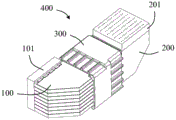
请参图1至图22所示,本发明揭示了一种电连接器组件400,其包括第一母端电连接器100、第二母端电连接器200以及用以连通所述第一母端电连接器100与所述第二母端电连接器200的转接器300。请参图1所示,在本发明图示的实施方式中,所述第一母端电连接器100具有用以安装于第一电路板101的第一安装面18,所述第二母端电连接器200具有用以安装于第二电路板201的第二安装面19,所述第一安装面18垂直于所述第二安装面19,所述第一电路板101垂直于所述第二电路板201。另外,根据端子设置的差异,第一母端电连接器100与第二母端电连接器200也可以分别为第一公端电连接器与第二公端电连接器。本发明具体实施方式中的第一母端电连接器100、第二母端电连接器200、第一公端电连接器与第二公端电连接器均被称之为电连接器。Referring to FIGS. 1 to 22, the present invention discloses an
请参图4至图14所示,所述第一母端电连接器100包括母端壳体10以及安装在所述母端壳体10上的若干母端端子模组20,所述若干母端端子模组20叠靠在一起。Referring to FIGS. 4 to 14 , the first receptacle
所述母端壳体10设有用以导引和定位所述若干母端端子模组20的导槽102、若干圆形的通孔103以及若干C形的通槽104,其中所述通孔103两两形成一组,相应的通槽104至少部分围绕在每组通孔103的外围。The
所述若干母端端子模组20的结构类似,以下仅选一组进行详细说明。The structures of the plurality of
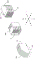
请参图9所示,所述母端端子模组20包括母端信号端子模组2以及与所述母端信号端子模组2相配合的接地件。在本发明的一种实施方式中,所述接地件为母端接地片3,其由金属材料加工成型,例如由金属板片冲压而成。所述母端信号端子模组2包括母端绝缘本体21以及安装在所述母端绝缘本体21上的信号端子。在本发明的一种实施方式中,所述信号端子为一对母端差分信号端子22。请参图7及图12所示,所述母端差分信号端子22包括母端接触部221,所述母端接地片3设有至少部分围绕在所述母端接触部221的外围的母端屏蔽部31。所述母端接触部221设有沿电连接器对接方向A-A延伸的弧形接触壁222,所述弧形接触壁222用以与对接端子相接触,所述对接端子可以是对接的连接器(例如转接器300)的端子。所述弧形接触壁222设有弧形内表面223,所述弧形内表面223用以与所述对接端子的外表面相接触。所述弧形接触壁222设有用以让所述对接端子插入的端子收容腔220,所述弧形内表面223围绕所述端子收容腔220。Referring to FIG. 9 , the
可以理解,在其他实施方式中,所述弧形接触壁222也可以设有弧形外表面,所述弧形外表面用以插入对接端子中以与对接端子的内表面相接触,同样可以实现端子接触的目的。It can be understood that, in other embodiments, the arc-shaped
具体地,请参图7及图12所示,所述母端差分信号端子22包括第一信号端子4以及第二信号端子5,所述第一信号端子4包括第一接触部41、第一尾部42以及连接所述第一接触部41与所述第一尾部42的第一连接部43,所述第二信号端子5包括第二接触部51、第二尾部52以及连接所述第二接触部51与所述第二尾部52的第二连接部53。所述母端接触部221包括所述第一接触部41以及所述第二接触部51,所述弧形接触壁222包括位于所述第一接触部41上的第一弧形接触壁411以及位于所述第二接触部51上的第二弧形接触壁511,所述第一弧形接触壁411至少为两个且相对设置,所述第二弧形接触壁511至少为两个且相对设置。所述端子收容腔220包括由两个所述第一弧形接触壁411所形成的第一端子收容腔2201以及由两个所述第二弧形接触壁511所形成的第二端子收容腔2202。Specifically, as shown in FIG. 7 and FIG. 12 , the female terminal
所述第一接触部41设有位于两个所述第一弧形接触壁411之间的两个第一狭槽412,两个所述第一狭槽412与所述第一端子收容腔2201相连通,使得所述第一接触部41具备一定的弹性变形能力,便于夹紧对接端子,提高二者的接触可靠性。类似地,所述第二接触部51设有位于两个所述第二弧形接触壁511之间的两个第二狭槽512,两个所述第二狭槽512与所述第二端子收容腔2202相连通,使得所述第二接触部51具备一定的弹性变形能力,便于夹紧对接端子,提高二者的接触可靠性。The
当然,在其他实施方式中,所述第一弧形接触壁411与所述第二弧形接触壁511也可以为一个,此时所述第一接触部41与所述第二接触部51的横截面大致呈C形、圆形、椭圆形等。Of course, in other embodiments, the first arc-shaped
所述第一连接部43与所述第一接触部41以及所述第二连接部53与所述第二接触部51之间设有第一交叉部44,所述第一连接部43与所述第一尾部42以及所述第二连接部53与所述第二尾部52之间设有第二交叉部45;其中:A
所述第一接触部41与所述第二接触部51沿固接方向B-B对齐布置,所述第一连接部43与所述第二连接部53沿所述母端信号端子模组2的厚度方向C-C对齐布置,所述第一尾部42与所述第二尾部52沿所述电连接器对接方向A-A对齐布置。在本发明图示的实施方式中,所述固接方向B-B为所述第一尾部42与所述第二尾部52插入电路板(如第一电路板101)的方向。当所述第一尾部42与所述第二尾部52插入到电路板上的安装孔后,可以通过焊接的方式与电路板进行固定以及电性连接。所述固接方向B-B、所述厚度方向C-C以及所述电连接器对接方向A-A相互垂直。The
请参图7所示,在本发明图示的实施方式中,每一个母端端子模组20的母端差分信号端子22有若干个并沿固接方向B-B排列为一排,每一个母端差分信号端子22的第一接触部41以及第二接触部51沿固接方向B-B排列为一排;然而,相邻的所述若干母端端子模组20的所述母端差分信号端子22的所述第一接触部41以及所述第二接触部51彼此错位布置。以图7来看,最左边第一直排的母端端子模组20的第一排母端差分信号端子22与最左边第二直排的母端端子模组的第二排母端差分信号端子22是在厚度方向C-C上彼此不对齐而形成错位布置,而不相邻的最左边第一直排的母端端子模组20的第一排母端差分信号端子22与最左边第三直排的母端端子模组的第三排母端差分信号端子22则可在厚度方向C-C上彼此对齐。通过相邻两个母端端子模组20的母端差分信号端子22彼此错位布置,可配合转接器300中的对接端子的扭转结构(容后详述),实现第一母端电连接器100与第二母端电连接器200的母端端子模组20中的母端差分信号端子22的90度转换结构。并且,也可降低相邻母端差分信号端子22之间的串扰。Referring to FIG. 7 , in the illustrated embodiment of the present invention, there are several female terminal
请参图11所示,所述母端信号端子模组2还包括固定在第一交叉部44上的第一定位块61以及固定在第二交叉部45上的第二定位块62,以将母端差分信号端子22形成为一个整体。Referring to FIG. 11 , the female
请参图9及图11所示,所述母端绝缘本体21设有第一端面211、第二端面212以及形成在所述第一端面211与所述第二端面212之间的若干沟槽213。所述沟槽213包括第一直线部2131、第二直线部2132以及连通所述第一直线部2131与所述第二直线部2132的倾斜部2133。在本发明图示的实施方式中,所述第一直线部2131沿所述对接方向A-A(例如水平方向)延伸,所述第二直线部2132沿所述固接方向B-B(例如竖直方向)延伸。所述沟槽213内设有金属层2130,每一对母端差分信号端子22位于相应的沟槽213中。所述沟槽213设有靠近所述第一端面211的第一安装槽2134以及靠近所述第二端面212的第二安装槽2135。从另一角度看,请参图11所示,所述母端绝缘本体21设有侧面210,所述沟槽213沿着所述厚度方向C-C贯穿所述侧面210,所述沟槽213用以收容所述第一连接部43与所述第二连接部53。所述母端接地片3覆盖所述侧面210,所述金属层2130与所述母端接地片3共同环绕所述第一连接部43与所述第二连接部53,以增强屏蔽效果,提高信号传输的质量。所述若干母端端子模组20沿厚度方向C-C叠靠,所述母端绝缘本体21的所述第一端面211朝向电连接器对接方向A-A且所述第二端面212朝向固接方向B-B。请参图16所示,相邻的所述若干母端端子模组20的所述第一安装槽2134在所述厚度方向C-C上彼此错位布置。所述母端差分信号端子22的所述第一接触部41以及所述第二接触部51是自对应的所述第一安装槽2134露出,相应地,相邻的所述若干母端端子模组20的所述母端差分信号端子22的所述第一接触部41以及所述第二接触部51在所述厚度方向C-C上彼此错位布置。Referring to FIG. 9 and FIG. 11 , the female terminal insulating
请参图9至图11所示,所述母端接地片3还设有与所述母端屏蔽部31相连的主体部32以及自所述主体部32向下(平行固接方向B-B)延伸的若干安装脚33。所述母端屏蔽部31自所述主体部32沿电连接器对接方向A-A延伸并部份围绕在所述母端接触部221的外围,所述母端屏蔽部31设有分别位于所述第一接触部41的上方的第一弹片311以及位于所述第二接触部51的下方的第二弹片312,以提高与对接连接器配合时的可靠性。Referring to FIGS. 9 to 11 , the
安装时,所述第一定位块61安装在第一安装槽2134中,所述第二定位块62安装在第二安装槽2135中。如此设置,一方面能够将第一信号端子4以及第二信号端子5安装到母端绝缘本体21上;另一方面通过所述第一定位块61以及所述第二定位块62能够有效避免第一信号端子4以及第二信号端子5与所述金属层2130发生接触。所述第一连接部43通过所述第一安装槽2134连接所述第一接触部41,并通过所述第二安装槽2135连接所述第一尾部42。所述第二连接部53通过所述第一安装槽2134连接所述第二接触部51,并通过所述第二安装槽2135连接所述第二尾部52。During installation, the
所述主体部32覆盖在所述沟槽213的外侧,通过所述金属层2130以及所述主体部32能够给母端差分信号端子22提供更好包裹,从而实现更好的屏蔽效果。优选地,所述金属层2130与所述母端接地片3相接触,从而增大屏蔽面积,提高屏蔽效果。The
在本发明的一种实施方式中,所述母端绝缘本体21由塑胶材料制成,所述金属层2130涂布在所述沟槽213内。在一些实施例中,所述金属层2130是以电镀方式涂布在所述沟槽213内。在其他实施方式中,所述第一母端电连接器100还包括若干塑胶件,所述塑胶件覆盖对应的母端绝缘本体21的所述侧面210,所述接地件为涂布于所述塑胶件的屏蔽层,所述屏蔽层位于所述塑胶件上靠近所述沟槽213的一侧。即,所述母端接地片3也可以由电镀了屏蔽层的塑胶件来替换。In an embodiment of the present invention, the female terminal insulating
所述在本发明图示的实施方式中,所述若干安装脚33自所述主体部32弯折延伸而偏离所述主体部32,即所述安装脚33与所述主体部32不在同一个平面内。请参图8所示,所述安装脚33、所述第一尾部42以及所述第二尾部52均沿所述电连接器对接方向A-A对齐布置(即排列为一排),便于将其安装到第一电路板101上且能够改善母端接地片3对母端差分信号端子22的屏蔽效果。In the illustrated embodiment of the present invention, the plurality of mounting
请参图15至图17所示,所述第二母端电连接器200具有与第一母端电连接器100相同或者类似的技术特征,所属技术领域的技术人员能够参考第一母端电连接器100来理解第二母端电连接器200。优选地,所述第一母端电连接器100与所述第二母端电连接器200为相同的电连接器,但是安装角度不同。如此设置,可以降低开模数量,降低成本。为此,在本发明图示的实施方式中,所述第一母端电连接器100与所述第二母端电连接器200中对应的特征采用相同的元件符号。Referring to FIGS. 15 to 17 , the second receptacle
请参图18至图22所示,所述转接器300包括转接器绝缘本体7、安装在所述转接器绝缘本体7上的若干转接器导电端子8以及与所述若干转接器导电端子8相配合的若干转接器接地片9。Referring to FIGS. 18 to 22 , the
所述转接器绝缘本体7包括用以与第一母端电连接器100相配合的第一收容腔71以及用以与第二母端电连接器200相配合的第二收容腔72。所述转接器导电端子8包括延伸入所述第一收容腔71中的第一对接部81、延伸入所述第二收容腔72中的第二对接部82以及位于所述第一对接部81与所述第二对接部82之间的扭转部83。所述转接器接地片9包括至少部分围绕在所述第一对接部81的外围的第一屏蔽壳体91以及至少部分围绕在所述第二对接部82的外围的第二屏蔽壳体92。当所述第一母端电连接器100以及所述第二母端电连接器200与所述转接器300连接后,可以理解,所述第一屏蔽壳体91以及所述第二屏蔽壳体92分别与所述第一母端电连接器100的母端接地片3以及与所述第二母端电连接器200的母端接地片3接触,以增加接地面积,从而实现较好的屏蔽效果。The
具体地,请参图22所示,所述转接器导电端子8包括若干转接器差分信号端子80,每一对所述转接器差分信号端子80包括第一转接器信号端子801以及第二转接器信号端子802,其中所述第一转接器信号端子801与所述第二转接器信号端子802均包括所述第一对接部81、所述第二对接部82以及所述扭转部83,其中:Specifically, as shown in FIG. 22 , the adapter
所述第一转接器信号端子801的所述第一对接部81与所述第二转接器信号端子802的所述第一对接部81沿左右方向布置;所述第一转接器信号端子801的所述第二对接部82与所述第二转接器信号端子802的所述第二对接部82沿上下方向布置。The
以上实施例仅用于说明本发明而并非限制本发明所描述的技术方案,对本说明书的理解应该以所属技术领域的技术人员为基础,例如对“前”、“后”、“左”、“右”、“上”、“下”等方向性的描述,尽管本说明书参照上述的实施例对本发明已进行了详细的说明,但是,本领域的普通技术人员应当理解,所属技术领域的技术人员仍然可以对本发明进行修改或者等同替换,而一切不脱离本发明的精神和范围的技术方案及其改进,均应涵盖在本发明的权利要求范围内。The above embodiments are only used to illustrate the present invention and do not limit the technical solutions described in the present invention. The understanding of this specification should be based on those skilled in the art, such as "front", "rear", "left", " Directional descriptions such as "right", "up", "down", etc., although this specification has described the present invention in detail with reference to the above-mentioned embodiments, those of ordinary skill in the art should understand that those skilled in the art The present invention can still be modified or equivalently replaced, and all technical solutions and improvements that do not depart from the spirit and scope of the present invention should be included within the scope of the claims of the present invention.
Claims (10)
Priority Applications (1)
| Application Number | Priority Date | Filing Date | Title |
|---|---|---|---|
| CN202010155226.4A CN111370943A (en) | 2020-03-06 | 2020-03-06 | Electrical connector |
Applications Claiming Priority (1)
| Application Number | Priority Date | Filing Date | Title |
|---|---|---|---|
| CN202010155226.4A CN111370943A (en) | 2020-03-06 | 2020-03-06 | Electrical connector |
Publications (1)
| Publication Number | Publication Date |
|---|---|
| CN111370943A true CN111370943A (en) | 2020-07-03 |
Family
ID=71206506
Family Applications (1)
| Application Number | Title | Priority Date | Filing Date |
|---|---|---|---|
| CN202010155226.4A Pending CN111370943A (en) | 2020-03-06 | 2020-03-06 | Electrical connector |
Country Status (1)
| Country | Link |
|---|---|
| CN (1) | CN111370943A (en) |
Cited By (4)
| Publication number | Priority date | Publication date | Assignee | Title |
|---|---|---|---|---|
| CN112003054A (en) * | 2020-07-08 | 2020-11-27 | 番禺得意精密电子工业有限公司 | Electrical connector |
| CN113193407A (en) * | 2021-02-02 | 2021-07-30 | 中山得意电子有限公司 | Electrical connector |
| US20220094116A1 (en) * | 2020-09-21 | 2022-03-24 | Dongguan Luxshare Technologies Co., Ltd | Terminal module for easy determination of electrical performance and backplane connector thereof |
| CN114243387A (en) * | 2021-11-08 | 2022-03-25 | 中山得意电子有限公司 | Electrical connector |
-
2020
- 2020-03-06 CN CN202010155226.4A patent/CN111370943A/en active Pending
Cited By (5)
| Publication number | Priority date | Publication date | Assignee | Title |
|---|---|---|---|---|
| CN112003054A (en) * | 2020-07-08 | 2020-11-27 | 番禺得意精密电子工业有限公司 | Electrical connector |
| US20220094116A1 (en) * | 2020-09-21 | 2022-03-24 | Dongguan Luxshare Technologies Co., Ltd | Terminal module for easy determination of electrical performance and backplane connector thereof |
| US11646535B2 (en) * | 2020-09-21 | 2023-05-09 | Dongguan Luxshare Technologies Co., Ltd | Terminal module for easy determination of electrical performance and backplane connector thereof |
| CN113193407A (en) * | 2021-02-02 | 2021-07-30 | 中山得意电子有限公司 | Electrical connector |
| CN114243387A (en) * | 2021-11-08 | 2022-03-25 | 中山得意电子有限公司 | Electrical connector |
Similar Documents
| Publication | Publication Date | Title |
|---|---|---|
| CN113823958B (en) | Backboard connector assembly | |
| US12266892B2 (en) | Connectors and contacts for a single twisted pair of conductors | |
| CN111370890B (en) | Electrical connectors, adapters, and electrical connector assemblies | |
| TWI817130B (en) | Mating module and cable connector | |
| TWI858382B (en) | Electrical connector and assembly thereof | |
| TWI424638B (en) | Performance enhancing contact module assemblies | |
| US6431914B1 (en) | Grounding scheme for a high speed backplane connector system | |
| CN201397973Y (en) | Electric connector | |
| CN110854572B (en) | Connector | |
| TWI826872B (en) | Terminal module and backplane connector | |
| CN111370943A (en) | Electrical connector | |
| CN113131244A (en) | Electric connector and electric connector assembly | |
| CN110752486A (en) | Connector | |
| US20250233348A1 (en) | Couplers for single pair connectors | |
| TW202123547A (en) | Electrical connector | |
| CN111834824B (en) | Socket connector with ground bus connector | |
| CN113131248B (en) | Electrical connector | |
| CN114784548A (en) | electrical connector | |
| CN120999359A (en) | Electrical connectors | |
| CN115642418A (en) | Electrical connector and installation method thereof | |
| CN113839239A (en) | circuit board connection combination |
Legal Events
| Date | Code | Title | Description |
|---|---|---|---|
| PB01 | Publication | ||
| PB01 | Publication | ||
| SE01 | Entry into force of request for substantive examination | ||
| SE01 | Entry into force of request for substantive examination | ||
| RJ01 | Rejection of invention patent application after publication |
Application publication date: 20200703 |
|
| RJ01 | Rejection of invention patent application after publication |