CN111341816A - Display panel, display panel manufacturing method and display device - Google Patents
Display panel, display panel manufacturing method and display device Download PDFInfo
- Publication number
- CN111341816A CN111341816A CN202010167671.2A CN202010167671A CN111341816A CN 111341816 A CN111341816 A CN 111341816A CN 202010167671 A CN202010167671 A CN 202010167671A CN 111341816 A CN111341816 A CN 111341816A
- Authority
- CN
- China
- Prior art keywords
- film layer
- sub
- scattering
- quantum dot
- display panel
- Prior art date
- Legal status (The legal status is an assumption and is not a legal conclusion. Google has not performed a legal analysis and makes no representation as to the accuracy of the status listed.)
- Granted
Links
Images
Classifications
-
- H—ELECTRICITY
- H10—SEMICONDUCTOR DEVICES; ELECTRIC SOLID-STATE DEVICES NOT OTHERWISE PROVIDED FOR
- H10K—ORGANIC ELECTRIC SOLID-STATE DEVICES
- H10K59/00—Integrated devices, or assemblies of multiple devices, comprising at least one organic light-emitting element covered by group H10K50/00
- H10K59/30—Devices specially adapted for multicolour light emission
-
- H—ELECTRICITY
- H10—SEMICONDUCTOR DEVICES; ELECTRIC SOLID-STATE DEVICES NOT OTHERWISE PROVIDED FOR
- H10K—ORGANIC ELECTRIC SOLID-STATE DEVICES
- H10K50/00—Organic light-emitting devices
- H10K50/10—OLEDs or polymer light-emitting diodes [PLED]
- H10K50/11—OLEDs or polymer light-emitting diodes [PLED] characterised by the electroluminescent [EL] layers
- H10K50/115—OLEDs or polymer light-emitting diodes [PLED] characterised by the electroluminescent [EL] layers comprising active inorganic nanostructures, e.g. luminescent quantum dots
-
- H—ELECTRICITY
- H10—SEMICONDUCTOR DEVICES; ELECTRIC SOLID-STATE DEVICES NOT OTHERWISE PROVIDED FOR
- H10K—ORGANIC ELECTRIC SOLID-STATE DEVICES
- H10K50/00—Organic light-emitting devices
- H10K50/80—Constructional details
- H10K50/85—Arrangements for extracting light from the devices
- H10K50/854—Arrangements for extracting light from the devices comprising scattering means
-
- H—ELECTRICITY
- H10—SEMICONDUCTOR DEVICES; ELECTRIC SOLID-STATE DEVICES NOT OTHERWISE PROVIDED FOR
- H10K—ORGANIC ELECTRIC SOLID-STATE DEVICES
- H10K59/00—Integrated devices, or assemblies of multiple devices, comprising at least one organic light-emitting element covered by group H10K50/00
- H10K59/30—Devices specially adapted for multicolour light emission
- H10K59/35—Devices specially adapted for multicolour light emission comprising red-green-blue [RGB] subpixels
-
- H—ELECTRICITY
- H10—SEMICONDUCTOR DEVICES; ELECTRIC SOLID-STATE DEVICES NOT OTHERWISE PROVIDED FOR
- H10K—ORGANIC ELECTRIC SOLID-STATE DEVICES
- H10K59/00—Integrated devices, or assemblies of multiple devices, comprising at least one organic light-emitting element covered by group H10K50/00
- H10K59/30—Devices specially adapted for multicolour light emission
- H10K59/38—Devices specially adapted for multicolour light emission comprising colour filters or colour changing media [CCM]
Landscapes
- Physics & Mathematics (AREA)
- Optics & Photonics (AREA)
- Chemical & Material Sciences (AREA)
- Engineering & Computer Science (AREA)
- Crystallography & Structural Chemistry (AREA)
- Inorganic Chemistry (AREA)
- Nanotechnology (AREA)
- Optical Filters (AREA)
- Liquid Crystal (AREA)
Abstract
The embodiment of the present application provides a display panel, and this display panel includes: blue backlight unit, colored filter layer and quantum dot rete. The blue backlight module and the color filter layer are arranged oppositely. The color filter layer comprises a blue sub-pixel area, a red sub-pixel area and a green sub-pixel area which are adjacently arranged. The quantum dot film layer is arranged between the blue backlight module and the color filter layer, and comprises a red quantum dot film layer, a green quantum dot film layer and a scattering film layer which are adjacently arranged. The scattering film layer is arranged corresponding to the blue sub-pixel area, the red quantum dot film layer is arranged corresponding to the red sub-pixel area, and the green quantum dot film layer is arranged corresponding to the green sub-pixel area. The scattering film layer is provided with scattering particles and comprises at least two sub-scattering film layers which are stacked. By correspondingly forming a layered structure containing scattering particles with different sizes in the blue light sub-pixel area, the optical path and scattering of the blue light are increased, and the purpose of improving the viewing angle of the blue light is achieved.
Description
Technical Field
The present disclosure relates to the field of display technologies, and in particular, to a display panel, a display panel manufacturing method, and a display device.
Background
The QD-OLED technology uses a blue OLED (Quantum Dot-Organic Light-Emitting Diode) evaporated on the whole surface as a self-luminous source and is matched with red and green Quantum Dot pixels prepared by a wet method, so that full-color display is realized. In the QD-OLED, red and green light is generated by exciting red and green quantum dots by OLED blue light, and blue light is directly emitted from a backlight, which often causes the viewing angle of blue light to be much smaller than that of red and green light in an actual device.
Disclosure of Invention
The embodiment of the application provides a display panel, a display panel manufacturing method and a display device, which can improve a blue light visual angle.
The application provides a display panel, including: the backlight module comprises a blue backlight module, a color filter layer and a quantum dot film layer;
the blue backlight module and the color filter layer are arranged oppositely;
the color filter layer comprises a blue sub-pixel area, a red sub-pixel area and a green sub-pixel area which are arranged adjacently;
the quantum dot film layer is arranged between the blue backlight module and the color filter layer and comprises a red quantum dot film layer, a green quantum dot film layer and a scattering film layer which are arranged adjacently; the scattering film layer is arranged corresponding to the blue sub-pixel area, the red quantum dot film layer is arranged corresponding to the red sub-pixel area, and the green quantum dot film layer is arranged corresponding to the green sub-pixel area; the scattering film layer is provided with scattering particles and comprises at least two sub-scattering film layers which are stacked.
In some embodiments, the particle size of the scattering particles disposed in the sub-scattering film layer gradually decreases along a direction from the blue backlight module to the color filter layer.
In some embodiments, the scattering film layer includes a first sub-scattering film layer and a second sub-scattering film layer, the first sub-scattering film layer is disposed on a side close to the blue backlight module, and the second sub-scattering film layer is disposed on a side close to the color filter layer; the particle size of the scattering particles of the first sub-scattering film layer is larger than that of the scattering particles of the second sub-scattering film layer.
In some embodiments, the scattering particles of the first sub-scattering film layer have a particle size of 300nm to 3000nm, and the scattering particles of the second sub-scattering film layer have a particle size of 10nm to 200 nm.
In some embodiments, the scattering film layer includes three sub-scattering film layers sequentially stacked, and a particle size of the scattering particles disposed in the sub-scattering film layers gradually decreases along a direction from the blue backlight module to the color filter layer.
In some embodiments, the scattering particles have a particle size of 10nm to 3000 nm.
In some embodiments, the material used for the scattering particles is any one of titanium dioxide, silicone, or a combination thereof.
The application provides a display panel manufacturing method, which comprises the following steps:
providing a blue backlight module;
the blue backlight module is provided with a red quantum dot film layer, a green quantum dot film layer and a scattering film layer which are adjacently arranged to form the quantum dot film layer, wherein scattering particles are arranged in the scattering film layer, and the scattering film layer comprises at least two sub-scattering film layers which are arranged in a stacked mode;
the red sub-pixel area is arranged on one side, far away from the blue backlight module, of the red quantum dot film layer, the green sub-pixel area is arranged on one side, far away from the blue backlight module, of the green quantum dot film layer, the blue sub-pixel area is arranged on one side, far away from the blue backlight module, of the scattering film layer, and the red sub-pixel area, the green sub-pixel area and the blue sub-pixel area form a color filter layer.
In some embodiments, the disposing a scattering film layer on the blue backlight module includes:
arranging resin on the blue backlight module;
dispersing scattering particles in the resin;
curing the resin and the scattering particles to form a sub-scattering film layer;
at least two sub-scattering film layers are arranged in a stacked manner to form a scattering film layer.
An embodiment of the present application provides a display device, including: the display panel comprises an upper glass substrate, a lower glass substrate and a display panel; the upper glass substrate and the lower glass substrate are oppositely arranged, the display panel is arranged between the upper glass substrate and the lower glass substrate, and the display panel is the display panel.
The display panel that this application embodiment provided includes: blue backlight unit, colored filter layer and quantum dot rete. The blue backlight module and the color filter layer are arranged oppositely. The color filter layer comprises a blue sub-pixel area, a red sub-pixel area and a green sub-pixel area which are adjacently arranged. The quantum dot film layer is arranged between the blue backlight module and the color filter layer, and comprises a red quantum dot film layer, a green quantum dot film layer and a scattering film layer which are adjacently arranged. The scattering film layer is arranged corresponding to the blue sub-pixel area, the red quantum dot film layer is arranged corresponding to the red sub-pixel area, and the green quantum dot film layer is arranged corresponding to the green sub-pixel area. The scattering film layer is provided with scattering particles and comprises at least two sub-scattering film layers which are stacked. The scattering film layer corresponding to the blue light sub-pixel area is provided with the layered structure containing scattering particles with different sizes, so that the optical path and scattering of blue light are increased, and the purpose of improving the blue light visual angle is achieved.
Drawings
In order to more clearly illustrate the technical solutions in the embodiments of the present application, the drawings needed to be used in the description of the embodiments are briefly introduced below, and it is obvious that the drawings in the following description are only some embodiments of the present application, and it is obvious for those skilled in the art to obtain other drawings based on these drawings without creative efforts.
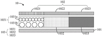
Fig. 1 is a schematic view of a first structure of a display panel according to an embodiment of the present disclosure;
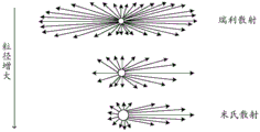
FIG. 2 is a schematic diagram illustrating the influence of the particle size of scattering particles on light scattering according to an embodiment of the present disclosure;
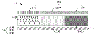
fig. 3 is a schematic view of a second structure of a display panel according to an embodiment of the present disclosure;
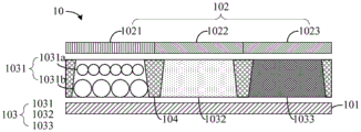
fig. 4 is a schematic structural diagram of a third display panel according to an embodiment of the present disclosure;
fig. 5 is a schematic diagram illustrating a fourth structure of a package structure according to an embodiment of the disclosure;
FIG. 6 is a first flowchart illustrating a method for fabricating a display panel according to an embodiment of the present disclosure;
fig. 7 is a schematic view of a first structure of a display device according to an embodiment of the present disclosure;
fig. 8 is a schematic view of a second structure of a display device according to an embodiment of the present application.
Detailed Description
The technical solutions in the embodiments of the present application will be clearly and completely described below with reference to the drawings in the embodiments of the present application. It is to be understood that the embodiments described are only a few embodiments of the present application and not all embodiments. All other embodiments, which can be derived by a person skilled in the art from the embodiments given herein without making any creative effort, shall fall within the protection scope of the present application.
It should be noted that in the description of the present application, it is to be understood that the terms "upper", "lower", "front", "rear", "left", "right", "inner", "outer", and the like indicate orientations or positional relationships based on the orientations or positional relationships shown in the drawings, which are only for convenience in describing the present application and simplifying the description, but do not indicate or imply that the referred device or element must have a specific orientation, be configured in a specific orientation, and operate, and thus, should not be construed as limiting the present application.
The embodiments of the present application provide a display panel, which is described in detail below.
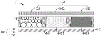
Referring to fig. 1, fig. 1 is a first structural schematic diagram of a display panel according to an embodiment of the present disclosure. The display panel 10 includes a blue backlight module 101, a color filter layer 102, and a quantum dot film layer 103. The blue backlight module 101 and the color filter layer 102 are disposed opposite to each other. The color filter layer 102 includes a blue sub-pixel area 1021, a red sub-pixel area 1022, and a green sub-pixel area 1023 disposed adjacent to each other. The quantum dot film layer 103 is disposed between the blue backlight module 101 and the color filter layer 102, and the quantum dot film layer 103 includes a red quantum dot film layer 1032, a green quantum dot film layer 1033, and a scattering film layer 1031 which are disposed adjacently. The scattering film 1031 is disposed corresponding to the blue sub-pixel 1021, the red quantum dot film 1032 is disposed corresponding to the red sub-pixel 1022, and the green quantum dot film 1033 is disposed corresponding to the green sub-pixel 1023. The scattering film 1031 is provided with scattering particles therein, and the scattering film 1031 includes at least two sub-scattering films stacked one on another.
In the display panel 10 provided by the embodiment of the application, the scattering membranous layer 1031 corresponding to the blue sub-pixel region 1021 is provided with at least two sub-scattering membranous layers which are stacked, the light emergent range and the path can be changed through the structure of the sub-scattering membranous layer, the structure of the sub-scattering membranous layer can be adjusted to increase the scattering optical path of blue backlight module emergent blue light, the blue light visual angle is improved, and the color cast of the display panel is reduced.
The particle size of the scattering particles disposed in the sub-scattering film layer gradually decreases along the direction from the blue backlight module 101 to the color filter layer 102. Referring to fig. 2, fig. 2 is a schematic diagram illustrating the influence of the particle size of the scattering particles on light scattering according to an embodiment of the present disclosure. As the particle size of the scattering particles becomes larger, the incident light gradually undergoes the conversion from rayleigh scattering to mie scattering. Therefore, by using this theory, the light path and scattering of the blue light are increased by providing the scattering film 1031 in which scattering particles with different particle sizes are continuously layered, so as to achieve the purpose of improving the viewing angle of the blue light.
The diffusion film 1031 includes a first sub-diffusion film 1031a and a second sub-diffusion film 1031b, the first sub-diffusion film 1031a is disposed on a side close to the blue backlight module 101, and the second sub-diffusion film 1031b is disposed on a side close to the color filter layer 102. The particle size of the scattering particles of the first sub scattering film layer 1031a is larger than the particle size of the scattering particles of the second sub scattering film layer 1031 b. Specifically, the particle size of the scattering particles of the first sub-scattering film layer 1031a is 300nm to 3000nm, and the particle size of the scattering particles of the second sub-scattering film layer 1031b is 10nm to 200 nm. Further, the scattering particles of the first sub-scattering film layer 1031a have a particle size of 300nm, 500nm, 700nm, 900nm, 1000nm, 1500nm, 2000nm, 2500nm, or 3000nm, and the scattering particles of the second sub-scattering film layer 1031b have a particle size of 10nm, 30nm, 50nm, 70nm, 90nm, 100nm, 150nm, or 200 nm.
Referring to fig. 3, fig. 3 is a schematic view of a second structure of a display panel according to an embodiment of the present disclosure. The scattering film 1031 includes three sub-scattering films sequentially stacked, and the particle size of the scattering particles in the sub-scattering films decreases gradually along the direction from the blue backlight module 101 to the color filter layer 102. The three sub-scattering film layers are stacked, and scattering of light can be better adjusted due to the fact that scattering particle size difference between the sub-scattering film layers is small. Further, the scattering film 1031 may further include four, five, or more than five sub-scattering films stacked on each other, and the particle size of the scattering particles in the sub-scattering films gradually decreases along the direction from the blue backlight module 101 to the color filter layer 102. The examples of the present application are illustrated by two layers and three layers, which are not intended to limit the embodiments of the present application.
Referring to fig. 4 and fig. 5, fig. 4 is a third structural schematic diagram of the display panel provided in the embodiment of the present application, and fig. 5 is a fourth structural schematic diagram of the display panel provided in the embodiment of the present application. The scattering film layer 1031 is separated from the red quantum dot film layer 1032 and the green quantum dot film layer 1033 by the pixel defining layer 104. The cross-sectional shape of the pixel defining layer 104 is a square or trapezoid. The manufacturing method for disposing the pixel defining layer 104 with square cross section is simple and convenient to operate. And the pixel definition layer 104 with the square cross section can leave a larger space for the scattering film layer, so that the scattering particles can be conveniently filled. The pixel definition layer 104 with the trapezoidal section can enable blue light which is not absorbed to be reflected back to excite the quantum dot light emitting layer again, and the light utilization rate is improved.
Wherein the scattering particles have a particle size of 10nm to 3000 nm. Specifically, the scattering particles have a particle diameter of 10nm, 30nm, 50nm, 70nm, 90nm, 100nm, 200nm, 300nm, 400nm, 500nm, 600nm, 700nm, 800nm, 900nm, 1000nm, 1500nm, 2000nm, 2500nm, or 3000 nm.
Wherein, the material adopted by the scattering particles is any one of titanium dioxide and organic silicon or the combination of the materials.
The scattering film 1031, the red quantum dot film 1032 and the green quantum dot film 1033 form a pixel unit. The display panel 10 includes at least one pixel unit. The scattering film layers 1031, the red quantum dot film layers 1032 and the green quantum dot film layers 1033 are alternately arranged, and the arrangement order and the arrangement mode are not limited.
The display panel 10 provided in the embodiment of the present application includes a blue backlight module 101, a color filter layer 102, and a quantum dot film layer 103. The quantum dot film layer 103 includes a red quantum dot film layer 1032, a green quantum dot film layer 1033, and a scattering film layer 1031, which are adjacently disposed. By disposing the scattering film 1031 with different particle sizes and continuously layering scattering particles corresponding to the blue sub-pixel region 1021, the particle sizes of the scattering particles gradually decrease along the direction from the blue backlight module 101 to the color filter layer 102. The scattering particles with large particle size close to the blue backlight module 101 generate Mie scattering, and the scattering and the collection of forward light are enhanced; small-particle-size scattering particles near the color filter layer 102 tend to rayleigh scatter, increasing the viewing angle of the light. Thereby increasing the optical path and scattering of the blue light and achieving the purpose of improving the viewing angle of the blue light.
The present invention provides a method for manufacturing a display panel, which is described in detail below. Referring to fig. 6, fig. 6 is a first flowchart illustrating a display panel manufacturing method according to an embodiment of the present disclosure.
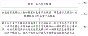
201. A blue backlight module is provided.
202. The blue backlight module is adjacently provided with a red quantum dot film layer, a green quantum dot film layer and a scattering film layer to form the quantum dot film layer.
The red quantum dot film layer and the green quantum dot film layer are arranged on the blue backlight module and are patterned by adopting a wet processing technology. And curing the red quantum dot film layer and the green quantum dot film layer. Specifically, the red quantum dot film layer and the green quantum dot film layer are subjected to thermal curing or photo-curing.
Wherein, a scattering film layer is arranged on the blue backlight module by adopting a wet processing technology. Specifically, resin is arranged on a blue backlight module, scattering particles are dispersed in the resin, and the resin and the scattering particles are cured to form a sub-scattering film layer; at least two sub-scattering film layers are stacked to form a scattering film layer. Specifically, the resin and the scattering particles are photo-cured or to form a sub-scattering film layer. The manufacturing method is convenient to operate, the setting operation of the sub-scattering film layers is controllable, the adjustment is easy, and the sub-scattering film layers are manufactured in a layered mode to form the scattering film layers, so that the particle size range of each sub-scattering film layer can be better guaranteed. In addition, the method for arranging the scattering film layer, the red quantum dot film layer and the green quantum dot film layer is a wet processing technology, so that the method can be carried out simultaneously, the production time is saved, and the production efficiency can be improved.
203. The red sub-pixel area is arranged on one side, far away from the blue backlight module, of the corresponding red quantum dot film layer, the green sub-pixel area is arranged on one side, far away from the blue backlight module, of the corresponding green quantum dot film layer, the blue sub-pixel area is arranged on one side, far away from the blue backlight module, of the corresponding scattering film layer, and the red sub-pixel area, the green sub-pixel area and the blue sub-pixel area form a color filter layer.
In the display panel manufacturing method provided by the embodiment of the application, the scattering film layer is arranged corresponding to the blue sub-pixel region by adopting a wet processing technology. Resin is arranged on the blue backlight module, scattering particles are dispersed in the resin, and the resin and the scattering particles are cured to form a sub-scattering film layer; at least two sub-scattering film layers are stacked to form a scattering film layer. The particle size of scattering particles in the sub-scattering film layer is gradually reduced along the direction from the blue backlight module to the color filter layer. Thereby increasing the optical path and scattering of the blue light and achieving the purpose of improving the viewing angle of the blue light.
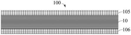
The embodiment of the present application provides a display device, which is described in detail below. Referring to fig. 7, fig. 7 is a schematic view illustrating a first structure of a display device 100 according to an embodiment of the present disclosure.
The display device 100 includes an upper glass substrate 105, a lower glass substrate 106, and a display panel 10. The upper glass substrate 105 and the lower glass substrate 106 are disposed opposite to each other, the display panel 10 is disposed between the upper glass substrate 105 and the lower glass substrate 106, and the display panel 10 is the display panel 10 described above.
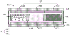
Referring to fig. 8, fig. 8 is a schematic diagram illustrating a second structure of the display device 100 according to the embodiment of the present disclosure. The display device 100 includes an upper glass substrate 105, a lower glass substrate 106, an encapsulation layer 107, and a display panel 10. The upper glass substrate 105 and the lower glass substrate 106 are disposed opposite to each other, the display panel 10 is disposed between the upper glass substrate 105 and the lower glass substrate 106, and the sealing layer 107 is disposed outside the display panel 10 and connects the upper glass substrate 105 and the lower glass substrate 106. The display panel 10 includes a blue backlight module 101, a color filter layer 102, and a quantum dot film layer 103. The blue backlight module 101 and the color filter layer 102 are disposed opposite to each other. The color filter layer 102 includes a blue sub-pixel area 1021, a red sub-pixel area 1022, and a green sub-pixel area 1023 disposed adjacent to each other. The quantum dot film layer 103 is disposed between the blue backlight module 101 and the color filter layer 102, and the quantum dot film layer 103 includes a red quantum dot film layer 1032, a green quantum dot film layer 1033, and a scattering film layer 1031 which are disposed adjacently. The scattering film 1031 is disposed corresponding to the blue sub-pixel 1021, the red quantum dot film 1032 is disposed corresponding to the red sub-pixel 1022, and the green quantum dot film 1033 is disposed corresponding to the green sub-pixel 1023. The scattering film 1031 is provided with scattering particles therein, and the scattering film 1031 includes at least two sub-scattering films stacked one on another.
The display device 100 may also include other devices, among others. The upper glass substrate 105, the lower glass substrate 106, the encapsulation layer 107 and other devices and their assembly in the embodiments of the present application are well known to those skilled in the art and will not be described in detail herein.
The display device provided by the embodiment of the application comprises an upper glass substrate 105, a lower glass substrate 106, an encapsulation layer 107 and a display panel 10. The display panel 10 includes a blue backlight module 101, a color filter layer 102, and a quantum dot film layer 103. The quantum dot film layer 103 includes a red quantum dot film layer 1032, a green quantum dot film layer 1033, and a scattering film layer 1031, which are adjacently disposed. By disposing the scattering film layer with different particle sizes continuously layered corresponding to the blue sub-pixel region 1021, the particle size of the scattering particles gradually decreases along the direction from the blue backlight module 101 to the color filter layer 102. The scattering particles with large particle size close to the blue backlight module 101 generate Mie scattering, and the scattering and the collection of forward light are enhanced; small-particle-size scattering particles near the color filter layer 102 tend to rayleigh scatter, increasing the viewing angle of the light. Thereby increasing the optical path and scattering of the blue light and achieving the purpose of improving the viewing angle of the blue light.
The display panel, the display panel manufacturing method and the display device provided in the embodiments of the present application are described in detail above, and specific examples are applied herein to explain the principles and embodiments of the present application, and the description of the embodiments above is only used to help understanding the present application. Meanwhile, for those skilled in the art, according to the idea of the present application, there may be variations in the specific embodiments and the application scope, and in summary, the content of the present specification should not be construed as a limitation to the present application.
Claims (10)
1. A display panel, comprising: the backlight module comprises a blue backlight module, a color filter layer and a quantum dot film layer;
the blue backlight module and the color filter layer are arranged oppositely;
the color filter layer comprises a blue sub-pixel area, a red sub-pixel area and a green sub-pixel area which are arranged adjacently;
the quantum dot film layer is arranged between the blue backlight module and the color filter layer and comprises a red quantum dot film layer, a green quantum dot film layer and a scattering film layer which are arranged adjacently; the scattering film layer is arranged corresponding to the blue sub-pixel area, the red quantum dot film layer is arranged corresponding to the red sub-pixel area, and the green quantum dot film layer is arranged corresponding to the green sub-pixel area; the scattering film layer is provided with scattering particles and comprises at least two sub-scattering film layers which are stacked.
2. The display panel according to claim 1, wherein the particle size of the scattering particles disposed in the sub-scattering film layer gradually decreases along a direction from the blue backlight module to the color filter layer.
3. The display panel according to claim 2, wherein the scattering film layers comprise a first sub-scattering film layer and a second sub-scattering film layer, the first sub-scattering film layer is disposed on a side close to the blue backlight module, and the second sub-scattering film layer is disposed on a side close to the color filter layer; the particle size of the scattering particles of the first sub-scattering film layer is larger than that of the scattering particles of the second sub-scattering film layer.
4. The display panel according to claim 3, wherein the scattering particles of the first sub-scattering film layer have a particle size of 300nm to 3000nm, and the scattering particles of the second sub-scattering film layer have a particle size of 10nm to 200 nm.
5. The display panel according to claim 1, wherein the scattering film layer comprises three sub-scattering film layers sequentially stacked, and a particle size of the scattering particles disposed in the sub-scattering film layers decreases gradually along a direction from the blue backlight module to the color filter layer.
6. The display panel according to claim 1, wherein the scattering particles have a particle size of 10nm to 3000 nm.
7. The display panel according to any one of claims 1 to 6, wherein a material used for the scattering particles is any one of titanium dioxide, silicone, or a combination of the above materials.
8. A method for manufacturing a display panel includes:
providing a blue backlight module;
the blue backlight module is provided with a red quantum dot film layer, a green quantum dot film layer and a scattering film layer which are adjacently arranged to form the quantum dot film layer, wherein scattering particles are arranged in the scattering film layer, and the scattering film layer comprises at least two sub-scattering film layers which are arranged in a stacked mode;
the red sub-pixel area is arranged on one side, far away from the blue backlight module, of the red quantum dot film layer, the green sub-pixel area is arranged on one side, far away from the blue backlight module, of the green quantum dot film layer, the blue sub-pixel area is arranged on one side, far away from the blue backlight module, of the scattering film layer, and the red sub-pixel area, the green sub-pixel area and the blue sub-pixel area form a color filter layer.
9. The display panel process method of claim 8, wherein disposing a scattering film on the blue backlight module comprises:
arranging resin on the blue backlight module;
dispersing scattering particles in the resin;
curing the resin and the scattering particles to form a sub-scattering film layer;
at least two sub-scattering film layers are arranged in a stacked manner to form a scattering film layer.
10. A display device, comprising: the display panel comprises an upper glass substrate, a lower glass substrate and a display panel; the upper glass substrate and the lower glass substrate are oppositely arranged, the display panel is arranged between the upper glass substrate and the lower glass substrate, and the display panel is the display panel of any one of claims 1 to 7.
Priority Applications (1)
| Application Number | Priority Date | Filing Date | Title |
|---|---|---|---|
| CN202010167671.2A CN111341816B (en) | 2020-03-11 | 2020-03-11 | Display panel, display panel manufacturing method and display device |
Applications Claiming Priority (1)
| Application Number | Priority Date | Filing Date | Title |
|---|---|---|---|
| CN202010167671.2A CN111341816B (en) | 2020-03-11 | 2020-03-11 | Display panel, display panel manufacturing method and display device |
Publications (2)
| Publication Number | Publication Date |
|---|---|
| CN111341816A true CN111341816A (en) | 2020-06-26 |
| CN111341816B CN111341816B (en) | 2022-11-25 |
Family
ID=71187975
Family Applications (1)
| Application Number | Title | Priority Date | Filing Date |
|---|---|---|---|
| CN202010167671.2A Active CN111341816B (en) | 2020-03-11 | 2020-03-11 | Display panel, display panel manufacturing method and display device |
Country Status (1)
| Country | Link |
|---|---|
| CN (1) | CN111341816B (en) |
Cited By (10)
| Publication number | Priority date | Publication date | Assignee | Title |
|---|---|---|---|---|
| CN111430570A (en) * | 2020-04-02 | 2020-07-17 | 深圳市华星光电半导体显示技术有限公司 | Display panel and method for manufacturing display panel |
| CN111863884A (en) * | 2020-07-01 | 2020-10-30 | 深圳市华星光电半导体显示技术有限公司 | Quantum dot color filter substrate and preparation method thereof, and display panel |
| CN112164709A (en) * | 2020-09-24 | 2021-01-01 | 武汉华星光电半导体显示技术有限公司 | Organic light emitting diode display panel, preparation method thereof and display device |
| CN112382733A (en) * | 2020-11-16 | 2021-02-19 | 京东方科技集团股份有限公司 | Flexible display panel, flexible display device and manufacturing method |
| CN112436097A (en) * | 2020-11-19 | 2021-03-02 | 合肥维信诺科技有限公司 | Display panel and preparation method thereof |
| CN113088129A (en) * | 2021-03-17 | 2021-07-09 | 深圳市华星光电半导体显示技术有限公司 | Scattered particle ink, display panel and display device |
| CN114384725A (en) * | 2021-12-30 | 2022-04-22 | 南京贝迪新材料科技股份有限公司 | Quantum dot composite film and preparation method thereof |
| CN115715102A (en) * | 2022-11-23 | 2023-02-24 | 惠科股份有限公司 | Quantum dot device and display device |
| US12349575B2 (en) | 2021-05-26 | 2025-07-01 | Boe Technology Group Co., Ltd. | Display panel, manufacture method therefor, and display device |
| US12523805B2 (en) | 2020-07-01 | 2026-01-13 | Shenzhen China Star Optoelectronics Semiconductor Display Technology Co., Ltd. | Quantum dot color filter substrate, manufacturing method thereof, and display panel |
Citations (6)
| Publication number | Priority date | Publication date | Assignee | Title |
|---|---|---|---|---|
| US20130320842A1 (en) * | 2012-05-31 | 2013-12-05 | Samsung Display Co., Ltd. | Organic light emitting display apparatus and method of manufacturing the same |
| CN106773306A (en) * | 2017-01-03 | 2017-05-31 | 青岛海信电器股份有限公司 | A kind of display panel and liquid crystal display device for being packaged with quantum dot layer |
| CN107153297A (en) * | 2017-07-21 | 2017-09-12 | 深圳市华星光电技术有限公司 | Display panel and display device |
| US20180088404A1 (en) * | 2016-09-28 | 2018-03-29 | Samsung Display Co., Ltd. | Color filter and display device including the same |
| CN110082848A (en) * | 2018-01-26 | 2019-08-02 | 中华映管股份有限公司 | Colored filter and liquid crystal display device including colored filter |
| CN110875360A (en) * | 2018-08-31 | 2020-03-10 | 昆山工研院新型平板显示技术中心有限公司 | Display panel |
-
2020
- 2020-03-11 CN CN202010167671.2A patent/CN111341816B/en active Active
Patent Citations (6)
| Publication number | Priority date | Publication date | Assignee | Title |
|---|---|---|---|---|
| US20130320842A1 (en) * | 2012-05-31 | 2013-12-05 | Samsung Display Co., Ltd. | Organic light emitting display apparatus and method of manufacturing the same |
| US20180088404A1 (en) * | 2016-09-28 | 2018-03-29 | Samsung Display Co., Ltd. | Color filter and display device including the same |
| CN106773306A (en) * | 2017-01-03 | 2017-05-31 | 青岛海信电器股份有限公司 | A kind of display panel and liquid crystal display device for being packaged with quantum dot layer |
| CN107153297A (en) * | 2017-07-21 | 2017-09-12 | 深圳市华星光电技术有限公司 | Display panel and display device |
| CN110082848A (en) * | 2018-01-26 | 2019-08-02 | 中华映管股份有限公司 | Colored filter and liquid crystal display device including colored filter |
| CN110875360A (en) * | 2018-08-31 | 2020-03-10 | 昆山工研院新型平板显示技术中心有限公司 | Display panel |
Cited By (14)
| Publication number | Priority date | Publication date | Assignee | Title |
|---|---|---|---|---|
| CN111430570A (en) * | 2020-04-02 | 2020-07-17 | 深圳市华星光电半导体显示技术有限公司 | Display panel and method for manufacturing display panel |
| WO2022000692A1 (en) * | 2020-07-01 | 2022-01-06 | 深圳市华星光电半导体显示技术有限公司 | Quantum dot color film substrate, preparation method therefor, and display panel |
| CN111863884A (en) * | 2020-07-01 | 2020-10-30 | 深圳市华星光电半导体显示技术有限公司 | Quantum dot color filter substrate and preparation method thereof, and display panel |
| US12523805B2 (en) | 2020-07-01 | 2026-01-13 | Shenzhen China Star Optoelectronics Semiconductor Display Technology Co., Ltd. | Quantum dot color filter substrate, manufacturing method thereof, and display panel |
| CN112164709A (en) * | 2020-09-24 | 2021-01-01 | 武汉华星光电半导体显示技术有限公司 | Organic light emitting diode display panel, preparation method thereof and display device |
| CN112382733A (en) * | 2020-11-16 | 2021-02-19 | 京东方科技集团股份有限公司 | Flexible display panel, flexible display device and manufacturing method |
| US12171109B2 (en) | 2020-11-16 | 2024-12-17 | Beijing Boe Technology Development Co., Ltd. | Flexible display panel, flexible display device and method of forming flexible display panel |
| CN112436097B (en) * | 2020-11-19 | 2023-03-24 | 合肥维信诺科技有限公司 | Display panel and preparation method thereof |
| CN112436097A (en) * | 2020-11-19 | 2021-03-02 | 合肥维信诺科技有限公司 | Display panel and preparation method thereof |
| CN113088129A (en) * | 2021-03-17 | 2021-07-09 | 深圳市华星光电半导体显示技术有限公司 | Scattered particle ink, display panel and display device |
| US12349575B2 (en) | 2021-05-26 | 2025-07-01 | Boe Technology Group Co., Ltd. | Display panel, manufacture method therefor, and display device |
| CN114384725A (en) * | 2021-12-30 | 2022-04-22 | 南京贝迪新材料科技股份有限公司 | Quantum dot composite film and preparation method thereof |
| CN115715102A (en) * | 2022-11-23 | 2023-02-24 | 惠科股份有限公司 | Quantum dot device and display device |
| CN115715102B (en) * | 2022-11-23 | 2023-10-20 | 惠科股份有限公司 | Quantum dot device and display device |
Also Published As
| Publication number | Publication date |
|---|---|
| CN111341816B (en) | 2022-11-25 |
Similar Documents
| Publication | Publication Date | Title |
|---|---|---|
| CN111341816B (en) | Display panel, display panel manufacturing method and display device | |
| CN115000322B (en) | Organic light-emitting display panel and display device | |
| EP3654383B1 (en) | Display device | |
| US10608054B2 (en) | Organic light-emitting diode (OLED) display and method of manufacturing the same | |
| CN110908168B (en) | display screen | |
| CN112614957B (en) | A display panel and a display device | |
| US11289544B2 (en) | Display device including wavelength conversion patterns having corresponding protruding and indentation pattern parts | |
| US9070889B2 (en) | OLED display having organic and inorganic encapsulation layers, and manufacturing method thereof | |
| CN102272974B (en) | Tiled OLED device with edge light extraction | |
| CN111540768B (en) | Color conversion substrate and display device | |
| CN101711439B (en) | Electroluminescent device having improved light output | |
| CN113261128A (en) | Display device | |
| CN106486509A (en) | Display device | |
| CN111403446B (en) | Display panel and manufacturing method thereof | |
| CN115360314A (en) | Display substrate, display device and manufacturing method | |
| US12119430B2 (en) | Color film substrate, method for preparing color film substrate, and display panel | |
| CN112310177A (en) | Display panel and preparation method thereof | |
| CN109755413B (en) | Display panel and preparation method thereof | |
| TW202324796A (en) | Light emitting devices including a color conversion material and light extracting structures and method of making thereof | |
| CN115954427A (en) | Micro light-emitting element and image display element | |
| CN115458566A (en) | Display panel, display device and method for manufacturing display panel | |
| US20210088844A1 (en) | Light-emitting module | |
| JP7049599B2 (en) | Display device | |
| KR20170020182A (en) | Qusntum Dot Light Conversion Device | |
| US11508706B2 (en) | Light-emitting module |
Legal Events
| Date | Code | Title | Description |
|---|---|---|---|
| PB01 | Publication | ||
| PB01 | Publication | ||
| SE01 | Entry into force of request for substantive examination | ||
| SE01 | Entry into force of request for substantive examination | ||
| GR01 | Patent grant | ||
| GR01 | Patent grant |