Processing method after laser cutting of chip
Technical Field
The invention relates to the technical field of chip cutting, in particular to a processing method of a laser-cut chip.
Background
In recent years, group iii-v semiconductors have become more widely used, and in order to greatly reduce cost and improve manufacturing efficiency, integrated circuit chips are often deposited on wafers in mass production, and then divided into units, and finally packaged and soldered. The wafer dicing technique has an important influence on the improvement of yield and packaging efficiency. The traditional cutting method comprises diamond scribing and cutting and wheel knife cutting, and the traditional cutting method has the following problems: 1. wide cutting grooves (30-100 um) and low wafer utilization rate; 2. cracks, fragments and delamination are easy to generate; 3. the cutter is worn quickly, a large amount of deionized water is consumed, the cost is increased, and the like. The laser cutting technology integrates optics, precision machinery, electronic technology and computer technology, and compared with the traditional processing method, the laser cutting method has the following advantages: 1. the processing speed is high; 2. the narrow cutting groove (10-30 um) has high wafer utilization rate; 3. non-contact processing is suitable for thin wafers; 4. high automation degree and arbitrary graph cutting. Therefore, the laser cutting technology gradually replaces the traditional cutting method and is applied.
Thermal stress is generated in the laser cutting process, and some burnt objects exist at the edge of the cut chip, so that the burnt objects are etched away by using a chemical etching method after cutting and then cleaned, the thermal stress is eliminated, and the mechanical strength of the chip is recovered. However, the conventional method has the following problems: 1) During the etching process, some burnt material particles can be suspended in the etching solution, and part of the burnt material particles can be adhered to the surface of the chip; 2) The surface of the etched wafer is provided with residual etching solution when leaving the etching solution, some burnt material particles exist in the residual etching solution, the etching solution can be rapidly concentrated on the lower half part of the chip and removed in the subsequent cleaning process due to the action of surface tension in the process of being transmitted to the cleaning link, so that the burnt material particles on the upper half part are attached to the surface of the chip, and the subsequent cleaning cannot be removed. The above problems cause a non-negligible loss of the yield of the appearance.
Disclosure of Invention
The invention aims to overcome the defects in the prior art and provides a processing method after laser cutting of a chip.
In order to achieve the above purpose, the technical scheme of the invention is as follows:
a processing method after laser cutting of a chip comprises the following steps:
1) Carrying out laser cutting and expanding treatment on the wafer to form a plurality of independent chips;
2) Soaking the chip in a surfactant solution;
3) Removing the chip from the surfactant solution, then immersing the chip in an etching solution, and etching the burnt material at the edge of the chip through the etching solution;
4) Cleaning the etched chip, and removing residual etching solution on the surface;
5) And drying the cleaned chip.
Preferably, in step 2), the surfactant solution comprises the following components:
a. 3-5wt% of polyethylene glycol, 2-4wt% of polyethylene glycol octyl phenyl ether and water as a solvent; b. 2-4wt% of polypropylene oxide and polyethylene oxide copolymer, 0.5-1.5wt% of polyoxyethylene compound and water as solvent; c. 9-11wt% of polyvinyl alcohol, 3-5wt% of ethoxy propoxylated-C6-12-alcohol and water as a solvent.
Preferably, in step 2), the chip is soaked in the surfactant solution for 60 to 180s.
Preferably, in the step 3), the chip is immersed in the etching solution for 30 to 60 seconds to perform etching.
Preferably, the etching solution comprises the following components: a. NH (NH) 4 ·H 2 O:H 2 O 2 :H 2 O =0.5-2:0.5-2:10 (volume ratio) mixed solution b, HCl: h 2 O 2 :H 2 O =0.5-2:0.5-2:1 (volume ratio); c. h 2 SO 4 :H 2 O 2 :H 2 O =4:1:1 (volume ratio);
preferably, in step 4), the chip is washed with deionized water.
Preferably, in the step 4), the etched chip is transferred to a fast draining flushing tank for flushing for 10-15min.
Preferably, in the step 5), the chip is baked at 45-65 ℃ for 10-60min.
Preferably, the chip is a GaAs chip, and the cutting is performed by adopting ultraviolet laser.
Preferably, the cutting power of the ultraviolet laser is 1-10W.
The beneficial effects of the invention are as follows:
after the chip is subjected to laser cutting and before etching, the wettability of the surface of the chip is improved by adopting a surfactant, so that the phenomenon that the burnt material particles adhere to the surface of the chip in the etching process is reduced; on the other hand, in the process of conveying the etched chip to the cleaning link, the etching solution remained on the surface of the chip keeps uniformly distributed on the surface of the chip, and the burnt material particles are still suspended in the remaining etching solution and cannot be attached to the surface of the chip, so that the burnt material particles are easily cleaned during subsequent cleaning. Therefore, the condition that the fused substance particles stay on the surface of the chip in the subsequent etching and cleaning process is improved, and the appearance yield of the product is improved.
Drawings
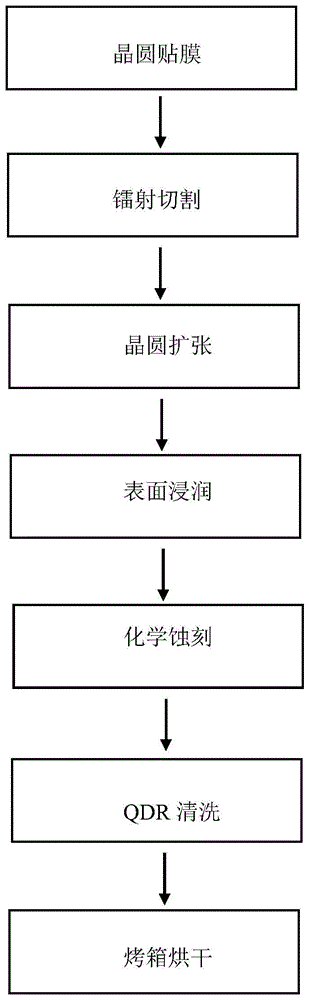
FIG. 1 is a process flow diagram of the present application.
In FIG. 2, a is a schematic diagram illustrating the variation of the residual etching solution on the surface of the chip in the comparative example; b is a schematic diagram of the change of the residual etching solution on the surface of the chip in the present application.
Detailed Description
The invention is further explained below with reference to the figures and the specific embodiments.
Referring to fig. 1, the processing method after the laser cutting of the chip of the present application includes the following steps:
wafer film pasting: pasting the back of the wafer on a UV film or a blue film with an iron ring;
laser cutting: cutting the wafer into independent chips by using laser, for example, for GaAs wafer, using UV laser, the laser power can be determined according to the thickness of the wafer, and is usually in the range of 1-10W; for example, a GaAs wafer with the thickness of 75-100um is cut by UV laser with the power of 3.4-5W;
expanding the wafer: expanding the film with the cut wafer to expand the distance between the chips;
surface infiltration: soaking the chip in a surfactant solution for 60-180s, wherein the surfactant solution comprises but is not limited to the following substances: a. 3-5wt% of polyethylene glycol, 2-4wt% of polyethylene glycol octyl phenyl ether and water as a solvent; b. 2-4wt% of polypropylene oxide and polyethylene oxide copolymer, 0.5-1.5wt% of polyoxyethylene compound and water as solvent; c. 9-11wt% of polyvinyl alcohol, 3-5wt% of ethoxy propoxylated-C6-12-alcohol and water as a solvent;
chemical etching: removing the chip from the surfactant solution, and soaking in an etching solution for 30-60s, wherein the etching solution includes but is not limited to the following: a. volume ratio NH 4 ·H 2 O:H 2 O 2 :H 2 O =0.5-2:0.5-2:10 of a mixed solution; b. the volume ratio of HCl: h 2 O 2 :H 2 O =0.5-2:0.5-2: 1; c. volume ratio H 2 SO 4 :H 2 O 2 :H 2 O =4:1: 1;
and (3) QDR cleaning: removing the chip from the etching solution, transferring to a quick-discharge washing tank, and washing with DI water for 10-15min;
oven drying: baking the cleaned chip at 45-65 ℃ for 10-60min.
Example 1
By adopting the method, the GaAs wafer with the thickness of 90um is cut by UV laser with the power of 4W, soaked in a surfactant solution for 100s after being cut, then soaked in an etching solution for 40s, transferred to a quick-discharge washing tank, washed by DI water for 10min, and baked in an oven at the temperature of 55 ℃ for 30min after being washed. Wherein the surfactant is: 83.8% of water, 4.1% of polyethylene glycol and 3.2% of polyethylene glycol octyl phenyl ether; the etching solution is ammonia water: hydrogen peroxide: water =1:1:10, and (b) a mixed solution.
Comparative example
The difference between the comparative example and example 1 is that there is no soaking step in surfactant solution, the cut wafer is directly put into the etching solution, and the rest steps and parameters are the same.
In example 1 and comparative example, when GaAs wafers are melted by high temperature under laser action, a part of the fused material remains at the edge of the cutting track, and the fused material has a main component: gaAs and its oxide, contain a small amount of UV colloidal carbide in the middle. In the process of etching by soaking in the etching solution, the reaction is as follows:
H 2 O 2 →H 2 O+O -
2GaAs+6O - →Ga 2 O 3 +As 2 O 3
NH 4 OH→NH 4 + +OH -
Ga 2 O 3 ·As 2 O 3 +12OH - →2AsO 3 3- +2GaO 3 3- +6H 2 O
as GaAs and oxides react with the etching solution, particles insoluble in the etching solution (hereinafter referred to as "burned material particles") such as carbides of UV paste are suspended in the etching solution. In example 1, the chip surface is processed after laser cutting and before etching, so that the wettability of the chip surface is improved, and the burn-in particles are prevented from sticking back to the chip surface after the wettability of the chip surface is improved. Whereas the comparative example had the phenomenon that the particles of the burnt-on material adhered back to the surface of the chip. Referring to fig. 2, when the chip is etched and leaves the etching solution, the surface of the chip has residual etching solution, and some burnt material particles exist in the residual etching solution, as shown in fig. 2a, in the comparative example, the etching solution is rapidly concentrated on the lower half portion of the chip due to the surface tension during the process of being transported to the cleaning link, so that the burnt material particles on the upper half portion are attached to the surface of the chip, the etching solution on the lower half portion is removed in the subsequent cleaning process, and the burnt material particles on the upper half portion cannot be removed; referring to fig. 2b, after the wettability of the chip surface is improved, the etching solution remaining on the chip surface remains uniformly distributed on the chip surface, and the burned substance particles still suspend in the remaining etching solution, and cannot adhere to the chip surface, and are easily cleaned during subsequent cleaning, so that the burned substance removal effect is improved.
Experiments show that the yield loss generated in the GaAs laser etching cleaning process is reduced by more than 50% in the embodiment 1 compared with the comparative embodiment. In addition, especially for the wafer with less chips, the yield rate can be greatly improved.
The above embodiments are only used to further illustrate the processing method after the laser cutting of the chip of the present invention, but the present invention is not limited to the embodiments, and any simple modifications, equivalent changes and modifications made to the above embodiments according to the technical essence of the present invention fall within the protection scope of the technical solution of the present invention.