The present application is a divisional application of the chinese patent application entitled "oxide nitride oxide stack with multiple oxynitride layers" with application number 201380016893.2.
This application is a continuation of co-pending U.S. application Ser. No. 11/811,958, filed 6/13/2007, which is incorporated herein by reference, in accordance with the priority of U.S. provisional patent application Ser. No. 60/931,947, filed 5/25/2007 in section 35 (e) of the code of U.S. code, both of which are incorporated herein by reference.
Brief Description of Drawings
These and various other features and advantages of the present structures and methods will become apparent upon reading the following detailed description and the appended claims, which are provided later, in conjunction with the accompanying drawings, in which:
FIG. 1 (prior art) is a block diagram showing a cross-sectional side view of an intermediate structure of a memory device with a method of forming an oxide-nitride-oxide (ONO) stack according to conventional methods;
fig. 2 is a block diagram illustrating a cross-sectional side view of a portion of a semiconductor device having a silicon oxide oxynitride silicon structure including a multi-layer charge storage layer in accordance with an embodiment of the present disclosure;
FIG. 3 is a flow chart diagram of a method of forming an oxide oxynitride oxide structure including a multi-layer charge storage layer according to an embodiment of the disclosure;
FIG. 4 is a graph illustrating improvements in data retention for a storage device using storage layers formed in accordance with the present disclosure as compared to a storage device using conventional storage layers;
FIG. 5 is a flow chart diagram of a method of forming an oxide oxynitride oxide structure including a multi-layer charge storage layer according to another embodiment of the present disclosure;
FIG. 6 is a band diagram of a programmed conventional memory device having an ONO structure;
fig. 7A and 7B are energy band diagrams of a memory device including multiple charge storage layers before and after programming according to an embodiment of the present disclosure;
FIG. 8A illustrates a non-planar multi-gate device including separate trapping regions;
FIG. 8B illustrates a cross-sectional view of the non-planar multi-gate device of FIG. 8A;
figures 9A and 9B illustrate a non-planar multi-gate device including a separate charge-trapping region and a horizontal nanowire channel.
FIGS. 10A and 10B illustrate a non-planar multi-gate device including a separate charge-trapping region and a vertical nanowire channel;
11A and 11B illustrate a first scheme of gates for fabricating the non-planar multi-gate device of FIG. 10A; and
fig. 12A and 12B illustrate a gate-last scheme for fabricating the non-planar multi-gate device of fig. 10A.
Detailed description of the invention
The present invention relates generally to an apparatus including a silicon oxide oxynitride silicon gate structure including a multi-layer charge storage layer and a method for fabricating the gate structure. The gate structure and method are particularly useful for forming a memory layer in a memory device, such as a memory transistor.
In the following description, for purposes of explanation, numerous specific details are set forth in order to provide a thorough understanding of the present disclosure. It will be apparent, however, to one skilled in the art that the present structures and methods may be practiced without these specific details. In other instances, well-known structures and techniques have not been shown in detail or in block diagram form in order to avoid unnecessarily obscuring the understanding of this description.
Reference in the specification to "one embodiment" or "an embodiment" means that a particular feature, structure, or characteristic described in connection with the embodiment is included in at least one embodiment. The appearances of the phrase "in one embodiment" in various places in the specification are not necessarily all referring to the same embodiment. The term "coupled" as used herein may include both a direct connection and an indirect connection through one or more intermediate components.
Briefly, the method involves forming a multi-layer charge storage layer comprising, for example, silicon oxynitride (Si)2N2O) layers having different concentrations of oxygen, nitrogen, and/or silicon. The oxynitride layer is formed at a higher temperature than the nitride or oxynitride layer in a conventional ONO structure and each layer is formed using a different process gas mixture and/or at a different flow rate. Typically, the oxynitride layer comprises at least a top oxynitride layer and a bottom oxynitride layer. In certain embodiments, the stoichiometric composition of the layers is tailored or selected such that the lower or bottom oxynitride has a high oxygen content and a silicon content, and the top oxynitride layer has a high silicon concentration and a high nitrogen concentration with a low oxygen concentration to produce an oxygen-depleted, silicon-rich nitride or oxynitride. The silicon-rich and oxygen-rich bottom oxynitride layers reduce the stored charge loss without affecting the device speed or the initial (onset of lifetime) difference between the program and erase voltages. The silicon-rich, oxygen-deficient top oxynitride layer increases the difference between the programming and erase voltages of the memory device, thereby increasing device speed, increasing data retention, and extending the operating life of the device. In some embodiments, the silicon-rich, oxygen-deficient top nitrogenThe oxide layer may also include a concentration of carbon selected to increase the number of traps therein.
Alternatively, the ratio of the thicknesses between the top and bottom oxynitride layers may be selected to facilitate formation of the oxynitride layer over the tunnel oxide layer or the first oxide layer of the silicon oxide oxynitride silicon gate structure after formation of the first oxide layer using dry oxidation or wet oxidation.
Silicon oxide oxynitride silicon structures and methods related to fabricating the structures according to various embodiments of the present disclosure will now be described in more detail with reference to fig. 2 through 4.
Figure 2 is a block diagram illustrating a cross-sectional side view of a portion of a semiconductor memory device 200 having a silicon oxide oxynitride silicon gate structure including multiple charge storage layers, according to one embodiment. Referring to fig. 2, the memory device 200 includes a silicon oxide oxynitride silicon gate structure or gate stack 202 including a multi-layer charge storage layer 204 formed over a surface 206 of a silicon layer on a substrate or silicon substrate 208. In addition, the device 200 also includes one or more diffusion regions 210, such as source and drain regions or structures, aligned with the gate stack 202 and separated by a channel region 212. Typically, a silicon oxide oxynitride silicon gate structure includes a gate layer comprising silicon, such as a polysilicon or polycrystalline gate layer 214 formed on the multi-layer charge storage layer 204 and in contact with the multi-layer charge storage layer 204, and a silicon layer or portion of the substrate 208. The polycrystalline gate layer 214 is separated or electrically isolated from the substrate 208 by the multi-layer charge storage layer 204. The silicon oxide oxynitride silicon structure includes a thin lower oxide layer or tunnel oxide layer 216 that separates or electrically isolates the gate stack 202 from the channel region 212, a top or blocking oxide layer 218, and a multi-layer charge storage layer 204. As described above and shown in fig. 2, the multi-layer charge storage layer 204 includes at least two oxynitride layers, including a top oxynitride layer 220A and a bottom oxynitride layer 220B.
Substrate 208 may comprise any well-known silicon-based semiconductor material including silicon, silicon-germanium, silicon-on-insulator, or silicon-on-sapphire substrates. Alternatively, the substrate 208 may include a silicon layer formed on a non-silicon-based semiconductor material, such as gallium arsenide, germanium, gallium nitride, or aluminum-phosphorous. In certain embodiments, the substrate 208 is a doped or undoped silicon substrate.
The lower oxide layer or
tunnel oxide layer 216 of the silicon oxide oxynitride silicon structure typically comprises from about 15 angstroms
To about
Relatively thin silicon dioxide (SiO)
2) A layer, and in some embodiments about
The
tunnel oxide layer 216 may be formed or deposited by any suitable means including, for example, thermally grown or deposited using Chemical Vapor Deposition (CVD). Thermal oxidation is typically used in an oxygen ambient to form or grow a tunnel oxide layer. In one embodiment, the process includes a dry oxidation process, wherein the
substrate 208 is placed in a deposition or processing chamber, heated to a temperature from about 700 ℃ to about 850 ℃, and exposed to oxygen for a predetermined period of time selected based on the desired thickness of the
tunnel oxide layer 216 achieved. In another embodiment, the tunnel oxide layer is grown in an ISSG (in situ steam generation) chamber using radical oxidation using oxygen (O) on the substrate
2) And hydrogen (H)
2) At a temperature of at least 1000 ℃. Exemplary processing times are from about 10 minutes to about 100 minutes. The oxidation may be performed at atmospheric or low pressure.
As described above, the multi-layer charge storage layer generally includes at least two oxynitride layers having different compositions of silicon, oxygen, and nitrogen, and the multi-layer charge storage layer may have an overall thickness of from about
To about
And in some embodiments is about
In one embodiment, the oxynitride layer is formed or deposited in a low pressure CVD process using a silicon source, such as silane (SiH4), chlorosilane (SiH) and an oxygen-containing gas
3Cl), dichlorosilane or DCS (SiH)
2Cl
2) Silicon tetrachloride (SiCl)
4) Di-tert-butylaminosilane (BTBAS), nitrogen sources such as nitrogen (N2), ammonia (NH)
3) Nitrogen trioxide (NO)
3) Or dinitrogen monoxide (N)
2O) containing oxygen, e.g. oxygen (O)
2) Or N
2And O. Alternatively, gases in which hydrogen has been replaced by deuterium may be used, including, for example, replacing NH
3Deuterated ammonia (ND)
3). Deuterium replacing hydrogen advantageously passivates Si dangling bonds at the silicon oxide interface, thereby increasing the NBTI (negative bias temperature instability) lifetime of the device.
For example, by placing the substrate 208 in a deposition chamber and introducing a gas containing N2O、NH3And DCS process gases while maintaining the chamber at a pressure of from about 5 millitorr (mT) to about 500mT and maintaining the substrate at a temperature of from about 700 c to about 850 c (and in some embodiments at a temperature of at least about 760 c) for a period of time of from about 2.5 minutes to about 20 minutes, a lower or bottom oxynitride layer 220B may be deposited over the tunnel oxide layer 216. In particular, the process gas may comprise at least one of from about 8: 1 to about 1: 8 ratio of mixed N2O and NH3And a first gas mixture of from about 1:7 to about 7: 1 ratio of DCS and NH3And may be introduced at a flow rate of from about 5 to 200 standard cubic centimeters per minute (sccm). It has been found that the creation of an oxynitride layer, generated or deposited under these conditions, occurs after programming anda silicon-rich, oxygen-rich bottom oxynitride layer 220B that reduces the rate of charge loss after erase, which exhibits a small voltage drift in the retention mode.
The top oxynitride layer 220A may be deposited over the bottom oxynitride layer 220B in a CVD process using a CVD process including N at a chamber pressure of from about 5mT to about 500mT and at a substrate temperature of from about 700 c to about 850 c (and in some embodiments at least about 760 c)2O、NH3And DCS for a period of time of about 2.5 minutes to about 20 minutes. In particular, the process gas may comprise at least one of from about 8: 1 to about 1: 8 proportions of N2O and NH3 and a first gas mixture in a ratio of from about 1:7 to about 7: a second gas mixture of DCS and NH3 mixed at a ratio of 1, and may be introduced at a flow rate of from about 5 to about 20 seem. It has been found that the oxynitride layer created or deposited under these conditions produces a silicon-rich, nitrogen-rich, and oxygen-lean top oxynitride layer 220A that increases speed and increases the initial difference between program and erase voltages without affecting the charge loss rate of memory devices fabricated using embodiments of the silicon oxide oxynitride silicon structure, thereby extending the operating life of the device.
In some embodiments, silicon-rich, nitrogen-rich, and oxygen-lean top oxynitride layer 220A may be deposited on bottom oxynitride layer 220B in a CVD process using a CVD process including etching from about 7: 1 to about 1:7 ratio of BTBAS and Ammonia (NH)3) To further include a concentration of carbon selected to increase the number of traps therein. The selected concentration of carbon in the second oxynitride layer may comprise a carbon concentration of from about 5% to about 15%.
In some embodiments, the top oxynitride layer 220A is deposited sequentially in the same tool used to form the bottom oxynitride layer 220B without substantially breaking the vacuum on the deposition chamber. In some embodiments, top oxynitride layer 220A is deposited without substantially changing the temperature to which substrate 208 is heated during deposition of bottom oxynitride layer 220B. In one embodiment, top oxynitride layer 220A is formedSequentially deposited and followed by reduction of N2O/NH3Gas mixture vs. DCS/NH3The flow rate of the gas mixture deposits the bottom oxynitride layer 220B to provide a gas mixture of desired ratios to produce the silicon-rich, nitrogen-rich, and oxygen-lean top oxynitride layer 220A.
In some embodiments, another oxide or oxide layer (not shown in these figures) is formed in a different region on the substrate 208 after forming the gate stack 202 or in a device that uses steam oxidation. In this embodiment, the top oxynitride layer 220A and the top or barrier oxide layer 218 of the silicon oxide oxynitride silicon structure are advantageously vapor annealed during the vapor oxidation process. In particular, the vapor anneal improves the quality of the top or barrier oxide layer 218, reduces the number of traps formed near the top surface of the barrier oxide layer, and reduces the number of traps formed near the top surface of the underlying top oxynitride layer 220A, thereby reducing or substantially eliminating the electric field that may otherwise form across the barrier oxide layer, which may cause the charge carriers to flow back therethrough and adversely affect data retention or charge retention in the charge storage layer.
Suitable thicknesses for
bottom oxynitride layer 220B have been found to be from about
To about
The ratio of the thicknesses between the bottom layer and the top oxynitride layer has been found to be from about 1: 6 to about 6: 1, and in certain embodiments, the ratio of the thicknesses between the bottom layer and the top oxynitride layer is at least about 1: 4.
the top or blocking
oxide layer 218 of the silicon oxide oxynitride silicon structure comprises from about
To about
Relatively thick SiO of
2The layer, and in some embodiments the top or
barrier oxide layer 218, comprises approximately
SiO of (2)
2And (3) a layer. The top or
barrier oxide layer 218 may be formed or deposited by any suitable means including, for example, thermally growing or using CVD. In one embodiment, the top or
barrier oxide layer 218 is a High Temperature Oxide (HTO) deposited using a CVD process. Typically, the deposition process includes exposing the
substrate 208 to a silicon source, such as silane, chlorosilane, or dichlorosilane, and an oxygen-containing gas, such as O, in a deposition chamber at a pressure of from about 50mT to about 1000mT
2Or N
2O) for a period of time of from about 10 minutes to about 120 minutes while maintaining the substrate at a temperature of from about 650 ℃ to about 850 ℃.
In some embodiments, the top or barrier oxide layer 218 is deposited sequentially in the same tool used to form the oxynitride layers 220A, 220B. In certain embodiments, the oxynitride layers 220A, 220B and the top or barrier oxide layer 218 are formed or deposited in the same tool used to grow the tunnel oxide layer 216. Suitable tools include, for example, ONO AVP commercially available from AVIZA technology of Stokes valley, California.
A method of forming or fabricating a silicon oxide oxynitride silicon stack according to one embodiment will now be described with reference to the flowchart of figure 3.
Referring to fig. 3, the method begins by forming a first oxide layer, such as a tunnel oxide layer 216, of a silicon oxide oxynitride silicon gate stack 202 over a silicon-containing layer on a surface of a substrate 208 (300). Next, a first or bottom oxynitride layer 220B of the multi-layer charge storage layer 204 comprising oxynitride is formed 302 on the surface of the first oxide layer. As aboveAs described, the first or bottom oxynitride layer 220B may be formed or deposited by a CVD process using a process gas containing N in a proportional and tailored flow rate2O/NH3And DCS/NH3A gas mixture to provide a silicon-rich and oxygen-rich oxynitride layer. A second or top oxynitride layer 220A of the multi-layer charge storage layer 204 is then formed 304 on the surface of the first or bottom oxynitride layer 220B. The second or top oxynitride layer 220A has a stoichiometric composition of oxygen, nitrogen, and/or silicon that is different from the stoichiometric composition of the first or bottom oxynitride layer 220B. In particular, and as described above, the second or top oxynitride layer 220A may be formed or deposited by a CVD process using a process gas containing a scaled and tailored flow rate of N2O/NH3And DCS/NH3A gas mixture to provide a silicon-rich, oxygen-depleted top oxynitride layer. Finally, a top or blocking oxide layer 218 of a silicon oxide oxynitride silicon structure is formed on a surface of the second layer of the multi-layer charge storage layer (306). As described above, the top or barrier oxide layer 218 may be formed or deposited in any suitable manner, but in some embodiments is deposited in a CVD process. In one embodiment, the top or barrier oxide layer 218 is a high temperature oxide deposited with an HTO CVD process. Optionally, the top or barrier oxide layer 218 may be thermally grown, however, it should be understood that in this embodiment, the thickness of the top oxynitride 220A may be adjusted or increased because some of the top oxynitride will be effectively consumed or oxidized during the process of thermally growing the top or barrier oxide layer 218.
Optionally, the method may further include forming or depositing a silicon-containing layer on the top or surface of the barrier oxide layer 218 to form a silicon oxide oxynitride silicon stack or structure (308). The silicon-containing layer may be, for example, a polysilicon layer deposited by a CVD process to form the control or poly gate layer 214 of the transistor or device 200.
A comparison will now be made with reference to fig. 4 of data retention for a storage device using a storage layer formed according to an embodiment of the present disclosure and a storage device using a conventional storage layer. In particular, fig. 4 shows the variation of threshold voltage of a device in an Electrically Erasable Programmable Read Only Memory (EEPROM) during programming (VTP) and during erasing (VTE) versus the life of the EEPROM device, where the EEPROM is made using a conventional ONO structure and using a silicon oxide oxynitride silicon structure with multiple oxynitride layers. In collecting data for this figure, both devices were pre-cycled for a 100K cycle at an ambient temperature of 85 ℃.
Referring to fig. 4, a graph or line 402 illustrates the VTP over time for an EEPROM fabricated using a conventional ONO structure having a single oxynitride layer without refreshing the memory after an initial write-program or erase. The actual data points on line 402 are shown by unfilled circles, with the remainder of the line showing an extrapolation of the VTP to a specified end of life (EOL) for the EEPROM. Graph or line 404 shows the change in VTE over time for an EEPROM fabricated using a conventional ONO structure. The actual data points on line 404 are shown by the filled circles and the rest of the line shows the extrapolation of the VTE to the EOL for the EEPROM. Typically, the specified difference between VTE and VTP for EEPROMs at EOL is at least 0.5V to enable identification and sensing of the difference between the programmed and erased states. As can be seen from the figure, the EEPROM fabricated using the conventional ONO structure has a difference between VTE and VTP of about 0.35V at a specified 20-year EOL. Thus, an EEPROM fabricated using a conventional ONO structure and operating under the conditions described above will not be able to meet a specified operating life of at least about 17 years.
In contrast, the variation in VTP and VTE over time for EEPROMs fabricated using silicon oxide oxynitride silicon structures having multiple oxynitride layers is shown by lines 406 and 408, respectively, showing the difference between VTE and VTP of at least about 1.96V for a specified EOL. Thus, an EEPROM fabricated using a silicon oxide oxynitride silicon structure in accordance with embodiments of the present disclosure will meet and exceed a specified operating life of 20 years. In particular, graph or line 406 illustrates the VTP over time for an EEPROM using a silicon oxide oxynitride silicon structure in accordance with an embodiment of the present disclosure. The actual data points on line 406 are represented by unfilled squares, with the remainder of the line showing the VTP extrapolation to the specified EOL. The graph or line 408 shows the change in VTE of the EEPROM over time, and the actual data points on line 408 are represented by filled squares, with the remainder of the line showing the extrapolation of VTE to EOL.
A method of forming or fabricating a semiconductor device according to another embodiment is now described with reference to the flowchart of fig. 5.
Referring to fig. 5, the method begins by forming a tunnel oxide layer 216 on a substrate (500). Next, an oxygen-rich, first or bottom oxynitride layer 220B of the multi-layer charge storage layer 204 is formed on the surface of the tunnel oxide layer 216 (502). As described above, the oxygen-rich, first or bottom oxynitride layer 220B may be formed by a CVD process using a CVD process that is comprised of from about 5: 1 to 15: 1 ratio of dichlorosilane (SiH)2Cl2) Ammonia gas (NH)3) Process gas of the mixture to form or deposit; and a pressure in the range from about 2: 1 to 4: 1 and nitrous oxide (N) at a tailored flow rate2O)/NH3A mixture to provide a silicon-rich and oxygen-rich oxynitride layer substantially free of traps. This is the stoichiometric composition of the first or bottom oxynitride layer 220B including a high concentration of oxygen selected to increase the retention properties of the multilayer charge storage layer by acting as a barrier between the charge trapped in the second or top oxynitride layer 220A and the substrate 208. The selected concentration of oxygen in the first or bottom oxynitride layer 220B may include an oxygen concentration of from about 15% to about 40%, and in some embodiments about 35%.
An oxygen-depleted, second or top oxynitride layer 220A is then formed on the surface of the first or bottom oxynitride layer 220B (504). The second or top oxynitride layer 220A has a stoichiometric composition of oxygen, nitrogen and/or silicon that is different from the stoichiometric composition of the first layer. In particular, and as described above, the second or top oxynitride layer 220A may be formed or deposited by a CVD process using a process gas that is comprised of a mixture of about 1: 6 to 1: 8 ratio range of N2O/NH3A mixture and a mixture of about 1.5: 1 to 3: 1 ratio range of SiH2Cl2/NH3Mixed to provide a trap density oxynitride layer having an oxygen concentration of about 5% or less. Thus, the second or top oxynitride layer 220A includes a charge trap density at least 1000 times greater than the charge trap density of the first or bottom oxynitride layer 220B.
Finally, a top or blocking oxide layer 218 is formed 506 over the second or top oxynitride layer 220A of the multi-layer charge storage layer 204. As described above, the top or barrier oxide layer 218 may be formed or deposited in any suitable manner. In one embodiment, second or barrier oxide layer 218 is formed in a manner that results in thinning second or top oxynitride layer 220A to a predetermined thickness by oxidizing a portion of the second oxynitride layer. Finally, as described above with reference to fig. 4, the improved retention performance of the multi-layer charge storage layer 204 increases the end of life (EOL) of the semiconductor device with respect to the specified difference between the program Voltage (VTP) and the erase Voltage (VTE) to at least about 20 years.
In another aspect, the multilayer charge storage layer of the present disclosure has a bandgap energy designed to generate an electric field opposite to that established due to charge storage in the charge storage layer in a programmed state, thereby increasing data retention without affecting programming voltage and/or device speed. Fig. 6 shows a band diagram of a conventional device programmed to include a channel in a silicon substrate 602, a tunnel oxide layer 604, a uniform nitride or oxynitride charge storage layer 606, an oxide blocking layer 608, and a polysilicon control gate 610. Referring to fig. 6, it should be noted that a large amount of trapped charge located near the center of the charge storage layer 606 results in the establishment of a large electric field away from the tunnel oxide layer 604 towards the trapped charge, and that it may cause or result in the loss of stored charge.
In contrast, in a memory device including the multilayer charge storage layer of the present disclosure, designing the band gap energy multilayer charge storage layer results in an electric field build-up directed inward (from the charge storage layer toward the tunnel oxide) that opposes the build-up of an electric field caused by the charge stored due to increased charge retention. An unprogrammed memory device including a multi-layer charge storage layer 706 is shown in fig. 7A. The apparatus includes a channel in a silicon substrate 702, a tunnel oxide layer 704, an oxygen-deficient oxynitride layer 706A, an oxygen-rich bottom oxynitride layer 706B, an oxide barrier layer 708, and a polysilicon control gate 710. Referring to fig. 7A, trap sites in the oxygen-deficient top oxynitride layer 706A create an electric field that opposes the electric field created by trapped charges in the programmed device. The bandgap diagram in the programmed state resulting in a device comprising a multi-layer charge storage layer 706 is shown in fig. 7A.
Embodiments and alternatives
In another aspect, the present disclosure relates to a multi-gate or multi-gate surface memory device including a charge-trapping region overlying two or more sides of a channel formed on or over a surface of a substrate and methods of fabricating the same. Multi-gate devices include both planar devices and non-planar devices. Planar multi-gate devices (not shown) typically include dual-gate planar devices, in which a large number of first layers are deposited to form a first gate beneath a subsequently formed channel, and a large number of second layers are deposited thereover to form a second gate. Non-planar multi-gate devices typically include a horizontal or vertical channel formed on or over a surface of a substrate and surrounded on three or more sides by a gate.
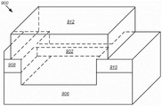
FIG. 8A illustrates one embodiment of a non-planar multi-gate memory device including a charge-trapping region. Referring to fig. 8A, a memory device 800, generally referred to as a finFET, includes a channel 802 formed by a thin film or layer of semiconductor material overlying a surface 804 on a substrate 806, which connects a source 808 and a drain 810 of the memory device. The channel 802 is surrounded on three sides by fins that form the gate 812 of the device. The thickness of the gate 812 (measured in the direction from source to drain) determines the effective channel length of the device.
In accordance with the present disclosure, the non-planar multi-gate memory device 800 of FIG. 8A may include separate charge-trapping regions. Fig. 8B is a cross-sectional view of a portion of the non-planar memory device of fig. 8A, including a portion of the substrate 806, the channel 802, and the gate 812, showing the multi-layer charge storage layer 814. The gate 812 also includes a tunnel oxide layer 816 covering the raised channel 802, a blocking dielectric 818, and a metal gate layer 820 covering the blocking layer to form a control gate for the memory device 800. In some embodiments, doped polysilicon may be deposited in place of metal to provide a polysilicon gate layer. The channel 802 and the gate 812 can be formed directly on the substrate 806 or directly on an insulating or dielectric layer 822, such as a buried oxide layer formed on or over the substrate.
Referring to FIG. 8B, the multi-layer charge storage layer 814 includes at least one lower or bottom charge-trapping layer 824 and an upper or top charge-trapping layer 826, the at least one lower or bottom charge-trapping layer 824 including nitride closer to the tunnel oxide layer 816, the upper or top charge-trapping layer 826 overlying the bottom charge-trapping layer. Typically, the top charge-trapping layer 826 comprises a silicon-rich, oxygen-poor nitride layer and includes a majority of the charge traps distributed among the plurality of charge-trapping layers, while the bottom charge-trapping layer 824 comprises an oxygen-rich nitride or silicon oxynitride and is oxygen-rich relative to the top charge-trapping layer to reduce the number of charge traps therein. By oxygen-rich, it is meant wherein the concentration of oxygen in the bottom charge-trapping layer 824 is from about 15% to about 40%, and the concentration of oxygen in the top charge-trapping layer 826 is less than about 5%.
In one embodiment, barrier dielectric 818 further comprises an oxide such as HTO to provide an ono structure. The channel 802 and overlying ono structure may be formed directly on the silicon substrate 806 and overlaid by a doped polysilicon gate layer 820 to provide a sononos structure.
In some embodiments, such as that shown in FIG. 8B, the multi-layer charge storage layer 814 further includes at least one thin intermediate or anti-tunneling layer 828 comprising a dielectric, such as an oxide, the at least one thin intermediate or anti-tunneling layer 828 separating the top and bottom charge-trapping layers 826 and 824. The anti-tunneling layer 828 substantially reduces the likelihood of electron charges accumulating at the boundary of the upper nitride layer 826 during programming from tunneling to the bottom nitride layer 824, resulting in a lower leakage current than that of the structures shown in fig. 1 and 6.
As with the embodiments described above, one or both of the bottom charge-trapping layer 824 and the top charge-trapping layer 826 may comprise silicon nitride or silicon oxynitride, and may be formed, for example, by a CVD process that includes N proportional and at a tailored flow rate2O/NH3And DCS/NH3The gas mixture to provide a silicon-rich and oxygen-rich oxynitride layer. A second nitride layer of the multi-layer charge storage structure is then formed on the intermediate oxide layer. The top charge-trapping layer 826 has a stoichiometric composition of oxygen, nitrogen, and/or silicon that is different from the stoichiometric composition of the bottom charge-trapping layer 824, and may also be formed or deposited by a CVD process using a CVD process that includes DCS/NH at a scaled and tailored flow rate3And N2O/NH3A process gas of the gas mixture to provide a silicon-rich, oxygen-depleted top nitride layer.
In those embodiments that include an intermediate comprising an oxide or anti-tunneling layer 828, the anti-tunneling layer may be formed by oxidizing the bottom oxynitride layer to a selected depth using free radical oxidation. Radical oxidation may be performed, for example, using a single wafer tool at a temperature of 1000-1100 deg.c, or using a batch reactor tool at a temperature of 800-900 deg.c. For batch processing, H can be used at pressures of 300-500 torr2And O2Mixtures of gases, or H using a single steam tool at a pressure of 10-15 torr2And O2A mixture of gases, using a single wafer tool for a period of 1 to 2 minutes, or using a batch process for a period of 30 minutes to 1 hour.
Finally, in those embodiments that include a barrier dielectric 818 that includes an oxide, the oxide may be formed or deposited in any suitable manner. In one embodiment, the oxide of barrier dielectric 818 is a high temperature oxide deposited in an HTO CVD process. Optionally, the barrier dielectric 818 or barrier oxide layer may be thermally grown, however it should be understood that in this embodiment, the top nitride thickness may be adjusted or increased because some of the top nitride will be effectively consumed or oxidized during the process of thermally growing the barrier oxide layer. A third option is to oxidize the top nitride layer to a selected depth using radical oxidation.
A suitable thickness for the bottom charge-
trapping layer 824 may be from about
To about
(with some allowable deviation, e.g. + -. 10A), of which
Can be consumed by radical oxidation to form the
anti-tunneling layer 828. A suitable thickness for the top charge-
trapping layer 826 may be at least
In some embodiments, the top charge-
trapping layer 826 may be formed up to
A thickness of (1), wherein
May be consumed by free radical oxidation to form
barrier dielectric 818. In some embodiments, the ratio of the thicknesses between the bottom charge-
trapping layer 824 and the top charge-
trapping layer 826 is about 1: 1, but other ratios are possible.
In other embodiments, one or both of the top charge-trapping layer 826 and the blocking dielectric 818 may comprise a high-K dielectric. Suitable high-K dielectrics include hafnium-based materials such as HfSiON, HfSiO, or HfO, zirconium-based materials such as ZrSiON, ZrSiO, or ZrO, and materials such as Y2O3Of (a) a yttrium-based material.
In another embodiment, shown in fig. 9A and 9B, a memory device may include a nanowire channel formed from a thin film of semiconductor material overlying a surface on a substrate, which connects a source and a drain of the memory device. By nanowire channel is meant a channel formed in a thin strip of crystalline silicon material having a maximum cross-sectional area of about 10 nanometers (nm) or less, and more preferably a maximum cross-sectional dimension of less than about 6 nm. Alternatively, the channel may be formed to have a <100> surface crystallographic orientation relative to the long axis of the channel.
Referring to fig. 9A, a memory device 900 includes a horizontal nanowire channel 902 formed from a thin film or layer of semiconductor material on or covering a surface on a substrate 906, the horizontal nanowire channel 902 connecting a source 908 and a drain 910 of the memory device. In the illustrated embodiment, the device has a gate-around (GAA) structure in which the nanowire channel 902 is surrounded on all sides by the gate 912 of the device. The thickness of gate 912 (measured in the source-to-drain direction) determines the effective channel length of the device.
In accordance with the present disclosure, the non-planar multi-gate memory device 900 of FIG. 9A may include separate charge-trapping regions. Figure 9B is a cross-sectional view of a portion of the non-planar memory device of figure 9A including a portion of the substrate 906, the nanowire channel 902, and the gate 912, showing a separate charge-trapping region. Referring to fig. 9B, the gate 912 includes a tunnel oxide layer 914 overlying the nanowire channel 902, a separate charge-trapping region, a blocking dielectric 916, and a gate layer 918 overlying the blocking layer to form a control gate of the memory device 900. The gate layer 918 may comprise a metal or doped polysilicon. The multi-layer charge storage layer includes at least one inner charge-trapping layer 920 and an outer charge-trapping layer 922, the inner charge-trapping layer 920 including a nitride closer to the tunnel oxide layer 914, the outer charge-trapping layer 922 covering the inner charge-trapping layer. Typically, the outer charge trapping layer 922 comprises a silicon-rich, oxygen-poor nitride layer and includes a majority of the charge traps distributed among the plurality of charge trapping layers, while the inner charge trapping layer 920 comprises an oxygen-rich nitride or silicon oxynitride and is oxygen-rich relative to the outer charge trapping layer to reduce the number of charge traps therein.
In some embodiments such as that shown, the multi-layer charge storage layer further includes at least one thin intermediate or anti-tunneling layer 924 comprising a dielectric such as an oxide, the at least one thin intermediate or anti-tunneling layer 924 separating the outer charge-trapping layer 922 and the inner charge-trapping layer 920. The anti-tunneling layer 924 substantially reduces the likelihood that electron charges will accumulate at the boundary of the outer charge-trapping layer 922 during programming from tunneling to the inner charge-trapping layer 920, resulting in a lower leakage current.
As with the embodiments described above, one or both of the inner charge-trapping layer 920 and the outer charge-trapping layer 922 may comprise silicon nitride or silicon oxynitride, and may be formed, for example, by a CVD process that includes N in proportion and at a tailored flow rate2O/NH3And DCS/NH3The gas mixture to provide a silicon-rich and oxygen-rich oxynitride layer. A second nitride layer of the multi-layer charge storage structure is then formed on the intermediate oxide layer. The outer charge-trapping layer 922 has a stoichiometric composition of oxygen, nitrogen and/or silicon that is different from the stoichiometric composition of the inner charge-trapping layer 920, and may also be formed or deposited by a CVD process using a CVD process that includes DCS/NH at a scaled and tailored flow rate3And N2O/NH3A process gas of the gas mixture to provide a silicon-rich, oxygen-depleted top nitride layer.
In those embodiments that include an intermediate or anti-tunneling layer 924 that includes an oxide, the anti-tunneling layer can be formed by oxidizing the internal charge-trapping layer 920 to a selected depth using free-radical oxidation. Radical oxidation may be performed, for example, using a single wafer tool at a temperature of 1000-1100 deg.c, or using a gap reactor tool at a temperature of 800-900 deg.c. For batch processing, H can be used at pressures of 300-500 torr2And O2Mixtures of gases, or H using a single steam tool at a pressure of 10-15 torr2And O2A mixture of gases, using a single wafer tool for a period of 1-2 minutes, or using a batch process for a period of 30 minutes to 1 hour.
Finally, in those embodiments where the barrier dielectric 916 comprises an oxide, the oxide may be formed or deposited in any suitable manner. In one embodiment, the oxide of barrier dielectric 916 is a high temperature oxide deposited in an HTO CVD process. Optionally, the blocking dielectric 916 or blocking oxide layer may be thermally grown, however it should be understood that in this embodiment, the thickness of the outer charge trapping layer 922 may need to be adjusted or increased because some of the top nitride will be effectively consumed or oxidized during the process of thermally growing the blocking oxide layer.
A suitable thickness for the inner charge-
trapping layer 920 may be from about
To about
(with some allowable deviation, e.g. + -. 10A), of which
Can be consumed by radical oxidation to form the
anti-tunneling layer 924. A suitable thickness for the outer
charge trapping layer 922 may be at least
In some embodiments, the outer
charge trapping layer 922 may be formed up to
A thickness of (1), wherein
May be consumed by free radical oxidation to form
barrier dielectric 916. In some embodiments, the ratio of the thicknesses between the inner charge-
trapping layer 920 and the outer charge-
trapping layer 922 is about 1: 1, but other ratios are possible.
In other embodiments, one or both of the outer charge trapping layer 922 and the blocking dielectric 916 may include a high K dielectric. Suitable high-K dielectrics include hafnium-based materials such as HfSiON, HfSiO, or HfO, zirconium-based materials such as ZrSiON, ZrSiO, or ZrOA material of, and for example Y2O3Of (a) a yttrium-based material.
In another embodiment, the memory device is or includes a non-planar device that includes a vertical nanowire channel formed on or from a semiconductor material that is on or protrudes from a bulk conductive, semiconductor layer on a substrate. In one variation of this embodiment, shown in cross-section in fig. 10A, the memory device 1000 includes a vertical nanowire channel 1002 formed in a cylinder of semiconductor material, the channel 1002 connecting a source 1004 and a drain 1006 of the device. The channel 1002 is surrounded by the tunnel oxide layer 1008, the multi-layer charge storage layer 1110, the blocking layer 1012, and the gate layer 1014 overlying the blocking layer to form a control gate for the memory device 1000. The trench 1002 may comprise an annular region in the outer layer of a substantially solid cylinder of semiconductor material, or may comprise an annular region formed over a cylinder of dielectric fill material. As with the horizontal nanowires described above, the channel 1002 can comprise polysilicon or recrystallized polysilicon to form a single crystalline channel. Alternatively, where the channel 1002 comprises crystalline silicon, the channel may be formed to have a <100> surface crystallographic orientation relative to the long axis of the channel.
In some embodiments, such as that shown in fig. 10B, the multi-layer charge storage layer 1010 may be a multi-layer charge storage layer including at least a first or inner charge-trapping layer 1016 and a second or outer charge-trapping layer 1018, the first or inner charge-trapping layer 1016 being closest to the tunnel oxide layer 1008. Optionally, the first charge trapping layer and the second charge trapping layer may be separated by an intermediate oxide or anti-tunneling layer 1020.
As with the embodiments described above, one or both of the first charge-trapping layer 1016 and the second charge-trapping layer 1018 may comprise silicon nitride or silicon oxynitride, and may be formed, for example, by a CVD process that includes N scaled and at a tailored flow rate2O/NH3And DCS/NH3The gas mixture to provide a silicon-rich and oxygen-rich oxynitride layer.
Finally, a second charge trapping layer 1018And barrier layer 1012 may include, for example, HfSiON, HfSiO, HfO, ZrSiON, ZrSiO, ZrO, or Y2O3High K dielectric.
A suitable thickness of the first
charge trapping layer 1016 may be from about
To about
(with some allowable deviation, e.g. + -. 10A), of which
Can be consumed by radical oxidation to form the
anti-tunneling layer 1020. A suitable thickness of the second charge-
trapping layer 1018 may be at least
And a suitable thickness for barrier dielectric 1012 may be from about
The memory device 1000 of fig. 10A may be fabricated using either the gate first scheme or the gate last scheme. Fig. 11A-F illustrate a first scheme of gates for fabricating the non-planar multi-gate device of fig. 10A. Fig. 12A-F illustrate a gate last scheme for fabricating the non-planar multi-gate device of fig. 10A.
Referring to fig. 11A, in a gate first scheme, a first or
lower dielectric layer 1102, such as a blocking oxide, is formed over a first
doped diffusion region 1104, such as a source or drain in a
substrate 1106. A
gate layer 1108 is deposited over the
first dielectric layer 1102 to form the control gate of the device and a second or
upper dielectric layer 1110 is formed thereover. As with the embodiments described above, the
first dielectric layer 1102 and the
second dielectric layer 1110 may be deposited by CVD, radical oxidation, or formed by oxidizing a portion of an underlying layer or substrate.
Gate layer 1108 may comprise a metal deposited by CVD or doped polysilicon deposited by CVD. In
generalGate layer 1108 is from about thick
And the thickness of the
first dielectric layer 1102 and the
second dielectric layer 1110 is from about
Referring to fig. 11B, a first opening 1112 is etched through the overlying gate layer 1108, and the first and second dielectric layers 1102, 1110 to a diffusion region 1104 in the substrate 1106. Next, layers including a tunnel oxide layer 1114, a multilayer charge storage layer 1116, and a blocking dielectric 1118 are sequentially deposited in the openings, and the surface of the upper dielectric layer 1110 is planarized to produce the intermediate structure shown in fig. 11C.
Although not shown, it is to be understood that, as in the embodiments described above, the multi-layer charge storage layer 1116 may include a multi-layer charge storage layer including at least a lower or bottom charge-trapping layer closer to the tunnel oxide layer 1114 and an upper or top charge-trapping layer overlying the bottom charge-trapping layer. Typically, the top charge-trapping layer comprises a silicon-rich, oxygen-poor nitride layer and includes a majority of the charge traps distributed in the plurality of charge-trapping layers, while the bottom charge-trapping layer comprises an oxygen-rich nitride or silicon oxynitride and is oxygen-rich relative to the top charge-trapping layer to reduce the number of charge traps therein. In some embodiments, the multi-layer charge storage layer 1116 also includes at least one thin intermediate or anti-tunneling layer comprising a dielectric such as an oxide, separating the top charge-trapping layer from the bottom charge-trapping layer.
Next, a second opening or channel opening 1120 is anisotropically etched through the tunnel oxide layer 1114, the multi-layer charge storage layer 1116 and the blocking dielectric 1118, fig. 11D. Referring to fig. 11E, a semiconductor material 1122 is deposited in the channel opening to form a vertical channel 1124 therein. The vertical channel 1124 can include an annular region in the outer layer of a substantially solid cylinder of semiconductor material, or, as shown in fig. 11E, can include a separate layer of semiconductor material 1122 surrounding a cylinder of dielectric fill material 1126.
Referring to fig. 11F, the surface of the upper dielectric layer 1110 is planarized and the layer of semiconductor material 1128 includes second doped diffusion regions 1130 (e.g., source and drain) formed therein deposited over the upper dielectric layer to form the illustrated device.
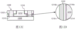
Referring to fig. 12, in a gate last scheme, a dielectric layer 1202, such as oxide, is formed over a sacrificial layer 1204 on a surface on a substrate 1206, an opening is etched through the dielectric layer and sacrificial layer, and a vertical channel 1208 is formed therein. As with the embodiments described above, the vertical channel 1208 may comprise an annular region in the outer layer of a substantially solid cylinder of semiconductor material 1210, such as polysilicon or monocrystalline silicon, or may comprise a separate layer of semiconductor material (not shown) surrounding a cylinder of dielectric fill material. The dielectric layer 1202 may comprise any suitable dielectric material, such as silicon oxide, capable of electrically isolating a subsequently formed gate layer of the memory device 1000 from an overlying electroactive layer or another memory device. The sacrificial layer 1204 may comprise any suitable material that may be etched or removed with high selectivity with respect to the materials of the dielectric layer 1202, the substrate 1206, and the vertical channels 1208.
Referring to fig. 12B, the second opening 1212 is etched by etching through the dielectric layer 1202 and the sacrificial layer 1204 to the substrate 1206, and the sacrificial layer 1204 is etched or removed. The sacrificial layer 1204 may comprise any suitable material that may be etched or removed with high selectivity with respect to the materials of the dielectric layer 1202, the substrate 1206, and the vertical channels 1208. In one embodiment, the sacrificial layer 1204 comprises silicon dioxide that can be removed by a buffered oxide etch (BOE etch).
Referring to fig. 12C and 12D, layers of tunnel oxide layer 1214, multilayer charge storage layer 1216, and blocking dielectric 1218 are sequentially deposited in the openings, and the surface of dielectric layer 1202 is planarized to produce the intermediate structure shown in fig. 12C and 12D. In some embodiments, such as shown in fig. 12D, the multi-layer charge storage layer 1216 may be a multi-layer charge storage layer that includes at least a first or inner charge-trapping layer 1216a and a second or outer charge-trapping layer 1216b, at least the first or inner charge-trapping layer 1216a being closest to the tunnel oxide layer 1214. Optionally, the first charge trapping layer and the second charge trapping layer may be separated by an intermediate oxide or anti-tunneling layer 1220.
Next, the gate layer 1222 is deposited into the second opening 1212, and the surface of the upper dielectric layer 1202 is planarized to produce the intermediate structure shown in fig. 12E. As with the embodiments described above, the gate layer 1222 may include a deposited metal or doped polysilicon. Finally, openings 1224 are etched through the gate layer 1222 to form control gates for the separated memory devices 1226.
Embodiments of the charge retention devices described herein may be implemented with logic circuitry to act as a machine memory. Those skilled in the art will appreciate that there are different logical implementations that can implement the described architecture, and that the preferred medium will vary with the environment in which the process is deployed. For example, if the implementer determines that speed and accuracy are paramount, the implementer may opt for a hardware and/or firmware vehicle; alternatively, if flexibility is paramount, the implementer may opt for a separate software implementation; or, yet alternatively, the implementer may opt for some combination of hardware, software, and/or firmware. Thus, there are many mediums in which the devices described herein can be implemented, none of which are fixedly superior to the others, as any medium to be utilized is selected based on the environment in which the medium is to be deployed and the particular concerns (e.g., speed, flexibility, or predictability) of the implementer, any of which may vary. Those skilled in the art will recognize that alternative aspects of the embodiments may comprise selectively oriented hardware, software, and or firmware.
Although shown or described above as having only two oxynitride layers, i.e., a top layer and a bottom layer, the present disclosure is not so limited and the multilayer charge storage layer may include any number n of oxynitride layers, any or all of which may have different stoichiometric compositions of oxygen, nitrogen, and/or silicon. In particular, multilayer charge storage layers having up to five oxynitride layers, each having a different stoichiometric composition, have been produced and tested. However, as will be appreciated by those skilled in the art, it is generally desirable to utilize as few layers as possible to achieve the desired results, to reduce the process steps necessary to manufacture the device, and thereby provide a simpler and more robust manufacturing process. Furthermore, using as few layers as possible also results in higher yields, since it is simpler to control the stoichiometric composition and size of fewer layers.
It should also be understood that although shown and described as part of a silicon oxide oxynitride silicon stack in a memory device, the structures and methods of the present disclosure are not so limited, and that silicon oxide oxynitride silicon structures may be used in or with any semiconductor technology or in any device requiring charge storage or requiring a dielectric layer or requiring a stack, including, for example, in split gate flash memory, a TaNOS stack, in 1T (transistor) SONOS type cells, 2T SONOS type cells, 3T SONOS type cells, local 2 bit cells, multi-level programming or cells, and/or 9T or 12T non-volatile semiconductor storage (NVSM) cells, without departing from the scope of the present disclosure.
The foregoing detailed description has set forth various embodiments of the devices and/or processes via the use of block diagrams, flowcharts, and/or examples. Insofar as such block diagrams, flowcharts, and/or examples include one or more functions and/or operations, it will be understood by those within the art that each function and/or operation within such block diagrams, flowcharts, or examples can be implemented, individually and/or collectively, by a wide range of hardware, software, firmware, or virtually any combination thereof.
Embodiments of the structures described herein may be implemented in an Application Specific Integrated Circuit (ASIC), a Field Programmable Gate Array (FPGA), a Central Processing Unit (CPU), a Digital Signal Processor (DSP), or other integrated form. However, those skilled in the art will recognize that certain aspects of the embodiments disclosed herein may be implemented equivalently, in whole or in part, in dedicated memory circuits, for the purpose of storing data and/or programs that run on one or more computers (e.g., as one or more programs running on one or more computer systems), as one or more programs running on one or more processors (e.g., as one or more programs running on one or more microprocessors), as firmware, or as virtually any combination thereof.
In a general sense, those skilled in the art will recognize that the various structures described herein can be implemented individually and/or collectively by a wide range of circuitry. As used herein, "electrical circuit" includes, but is not limited to, an electrical circuit having at least one discrete electrical circuit, an electrical circuit having at least one integrated circuit, an electrical circuit having at least one application specific integrated circuit, an electrical circuit forming a general purpose computing device configured by a computer program (e.g., a general purpose computer configured by a computer program that performs at least in part the processes and/or devices described herein, or a microprocessor configured by a computer program that performs at least in part the processes and/or devices described herein), an electrical circuit forming a memory device (e.g., in the form of random access memory), and/or an electrical circuit forming a communications device (e.g., a modem, a communications switch, or an optoelectronic device).
Those skilled in the art will recognize that in the manner set forth herein, devices and/or processes are described in a manner common in the art, and then standard engineering practices are used to integrate these described devices and/or processes into a larger system. That is, at least a portion of the devices and/or processes described herein may be integrated into a network processing system without undue experimentation.