CN111105823B - Semiconductor device - Google Patents

Semiconductor device Download PDF

Info

Publication number
CN111105823B
CN111105823B CN201910624347.6A CN201910624347A CN111105823B CN 111105823 B CN111105823 B CN 111105823B CN 201910624347 A CN201910624347 A CN 201910624347A CN 111105823 B CN111105823 B CN 111105823B
Authority
CN
China
Prior art keywords
signal
write
read
bank
address signal
Prior art date
Legal status (The legal status is an assumption and is not a legal conclusion. Google has not performed a legal analysis and makes no representation as to the accuracy of the status listed.)
Active
Application number
CN201910624347.6A
Other languages
Chinese (zh)
Other versions
CN111105823A (en
Inventor
金雄来
Current Assignee (The listed assignees may be inaccurate. Google has not performed a legal analysis and makes no representation or warranty as to the accuracy of the list.)
SK Hynix Inc
Original Assignee
SK Hynix Inc
Priority date (The priority date is an assumption and is not a legal conclusion. Google has not performed a legal analysis and makes no representation as to the accuracy of the date listed.)
Filing date
Publication date
Application filed by SK Hynix Inc filed Critical SK Hynix Inc
Publication of CN111105823A publication Critical patent/CN111105823A/en
Application granted granted Critical
Publication of CN111105823B publication Critical patent/CN111105823B/en
Active legal-status Critical Current
Anticipated expiration legal-status Critical

Links

Images

Classifications

    • GPHYSICS
    • G11INFORMATION STORAGE
    • G11CSTATIC STORES
    • G11C8/00Arrangements for selecting an address in a digital store
    • G11C8/12Group selection circuits, e.g. for memory block selection, chip selection, array selection
    • GPHYSICS
    • G11INFORMATION STORAGE
    • G11CSTATIC STORES
    • G11C8/00Arrangements for selecting an address in a digital store
    • G11C8/18Address timing or clocking circuits; Address control signal generation or management, e.g. for row address strobe [RAS] or column address strobe [CAS] signals
    • GPHYSICS
    • G11INFORMATION STORAGE
    • G11CSTATIC STORES
    • G11C11/00Digital stores characterised by the use of particular electric or magnetic storage elements; Storage elements therefor
    • G11C11/21Digital stores characterised by the use of particular electric or magnetic storage elements; Storage elements therefor using electric elements
    • G11C11/34Digital stores characterised by the use of particular electric or magnetic storage elements; Storage elements therefor using electric elements using semiconductor devices
    • G11C11/40Digital stores characterised by the use of particular electric or magnetic storage elements; Storage elements therefor using electric elements using semiconductor devices using transistors
    • G11C11/401Digital stores characterised by the use of particular electric or magnetic storage elements; Storage elements therefor using electric elements using semiconductor devices using transistors forming cells needing refreshing or charge regeneration, i.e. dynamic cells
    • G11C11/4063Auxiliary circuits, e.g. for addressing, decoding, driving, writing, sensing or timing
    • G11C11/407Auxiliary circuits, e.g. for addressing, decoding, driving, writing, sensing or timing for memory cells of the field-effect type
    • G11C11/408Address circuits
    • GPHYSICS
    • G11INFORMATION STORAGE
    • G11CSTATIC STORES
    • G11C7/00Arrangements for writing information into, or reading information out from, a digital store
    • G11C7/10Input/output [I/O] data interface arrangements, e.g. I/O data control circuits, I/O data buffers
    • G11C7/1015Read-write modes for single port memories, i.e. having either a random port or a serial port
    • G11C7/1039Read-write modes for single port memories, i.e. having either a random port or a serial port using pipelining techniques, i.e. using latches between functional memory parts, e.g. row/column decoders, I/O buffers, sense amplifiers
    • GPHYSICS
    • G11INFORMATION STORAGE
    • G11CSTATIC STORES
    • G11C7/00Arrangements for writing information into, or reading information out from, a digital store
    • G11C7/22Read-write [R-W] timing or clocking circuits; Read-write [R-W] control signal generators or management 
    • G11C7/222Clock generating, synchronizing or distributing circuits within memory device
    • GPHYSICS
    • G11INFORMATION STORAGE
    • G11CSTATIC STORES
    • G11C8/00Arrangements for selecting an address in a digital store
    • G11C8/06Address interface arrangements, e.g. address buffers

Landscapes

  • Engineering & Computer Science (AREA)
  • Microelectronics & Electronic Packaging (AREA)
  • Computer Hardware Design (AREA)
  • Dram (AREA)

Abstract

The invention discloses a semiconductor device. The semiconductor device includes a control circuit and an address generation circuit. The control circuit generates a write column address signal, a write bank select signal, and an internal write bank select signal from the command/address signal during a write operation. The control circuit also generates a read column address signal, a read bank select signal, and an internal read bank select signal from the command/address signal during a read operation. The address generation circuit outputs a write column address signal as a bank group address signal in synchronization with a write bank selection signal and an internal write bank selection signal, or outputs a read column address signal as a bank group address signal in synchronization with a read bank selection signal and an internal read bank selection signal.

Description

半导体器件Semiconductor device

相关申请的交叉引用Cross References to Related Applications

本申请要求于2018年10月29日提交的申请号为10-2018-0130179的韩国专利申请的优先权,其全部内容通过引用合并于此。This application claims priority from Korean Patent Application No. 10-2018-0130179 filed on October 29, 2018, the entire contents of which are hereby incorporated by reference.

技术领域technical field

本公开的实施例总体上涉及与列操作有关的半导体器件。Embodiments of the present disclosure generally relate to semiconductor devices related to column operations.

背景技术Background technique

通常,诸如动态随机存取存储器(DRAM)器件之类的半导体器件中的每个半导体器件可以包括多个存储体组,其由通过地址来选择的单元阵列组成。每个存储体组可以被实现为包括多个存储体。半导体器件可以选择多个存储体组中的任何一个,并且可以经由输入/输出(I/O)线来执行用于输出储存在所选存储体组中所包括的单元阵列中的数据的列操作。In general, each of semiconductor devices such as dynamic random access memory (DRAM) devices may include a plurality of bank groups consisting of cell arrays selected by addresses. Each bank group may be implemented to include a plurality of banks. The semiconductor device can select any one of a plurality of bank groups, and can perform a column operation for outputting data stored in a cell array included in the selected bank group via an input/output (I/O) line .

发明内容Contents of the invention

根据实施例,一种半导体器件包括控制电路和地址发生电路。控制电路在写入操作期间从命令/地址信号产生写入列地址信号,并且在写入操作期间从命令/地址信号产生写入存储体选择信号和内部写入存储体选择信号。控制电路还在读取操作期间从命令/地址信号产生读取列地址信号,并且在读取操作期间从命令/地址信号产生读取存储体选择信号和内部读取存储体选择信号。写入存储体选择信号和内部写入存储体选择信号被顺序地使能,并且其中读取存储体选择信号和内部读取存储体选择信号被顺序地使能。地址发生电路与写入存储体选择信号和内部写入存储体选择信号同步地输出写入列地址信号作为存储体组地址信号,或者与读取存储体选择信号和内部读取存储体选择信号同步地输出读取列地址信号作为存储体组地址信号。According to an embodiment, a semiconductor device includes a control circuit and an address generation circuit. The control circuit generates a write column address signal from a command/address signal during a write operation, and generates a write bank select signal and an internal write bank select signal from the command/address signal during a write operation. The control circuit also generates a read column address signal from the command/address signal during a read operation, and generates a read bank select signal and an internal read bank select signal from the command/address signal during the read operation. The write bank selection signal and the internal write bank selection signal are sequentially enabled, and wherein the read bank selection signal and the internal read bank selection signal are sequentially enabled. The address generation circuit outputs the write column address signal as a bank group address signal synchronously with the write bank select signal and the internal write bank select signal, or synchronously with the read bank select signal and the internal read bank select signal output the read column address signal as the bank group address signal.

根据实施例,一种半导体器件包括控制电路、地址发生电路和核心电路。控制电路在写入操作期间从命令/地址信号产生第一写入列地址信号和第二写入列地址信号、第一写入存储体选择信号和第二写入存储体选择信号、以及第一内部写入存储体选择信号和第二内部写入存储体选择信号。控制电路还在读取操作期间从命令/地址信号产生第一读取列地址信号和第二读取列地址信号、第一读取存储体选择信号和第二读取存储体选择信号、以及第一内部读取存储体选择信号和第二内部读取存储体选择信号。地址发生电路与第一写入存储体选择信号和第二写入存储体选择信号以及第一内部写入存储体选择信号和第二内部写入存储体选择信号同步地输出第一写入列地址信号和第二写入列地址信号作为第一存储体组地址信号和第二存储体组地址信号,或者与第一读取存储体选择信号和第二读取存储体选择信号以及第一内部读取存储体选择信号和第二内部读取存储体选择信号同步地输出第一读取列地址信号和第二读取列地址信号作为第一存储体组地址信号和第二存储体组地址信号。核心电路包括第一存储体组和第二存储体组。当第一存储体组地址信号被使能时,第一存储体组执行写入操作和读取操作,并且当第二存储体组地址信号被使能时,第二存储体组执行写入操作和读取操作。According to an embodiment, a semiconductor device includes a control circuit, an address generation circuit, and a core circuit. The control circuit generates a first write column address signal and a second write column address signal, a first write bank select signal and a second write bank select signal, and a first write bank select signal from the command/address signal during a write operation. An internal write bank select signal and a second internal write bank select signal. The control circuit also generates a first read column address signal and a second read column address signal, a first read bank selection signal and a second read bank selection signal, and a second read column address signal from the command/address signal during a read operation. An internal read bank select signal and a second internal read bank select signal. The address generation circuit outputs the first write column address synchronously with the first write bank select signal and the second write bank select signal and the first internal write bank select signal and the second internal write bank select signal signal and the second write column address signal as the first bank group address signal and the second bank group address signal, or with the first read bank select signal and the second read bank select signal and the first internal read Synchronously outputting the first read column address signal and the second read column address signal as the first bank group address signal and the second bank group address signal by taking the bank select signal and the second internal read bank select signal. The core circuit includes a first memory bank group and a second memory bank group. When the first bank group address signal is enabled, the first bank group performs write operation and read operation, and when the second bank group address signal is enabled, the second bank group performs write operation and read operations.

附图说明Description of drawings

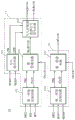
图1是示出根据本公开的实施例的半导体器件的配置的框图。FIG. 1 is a block diagram showing the configuration of a semiconductor device according to an embodiment of the present disclosure.

图2是示出图1的半导体器件中所包括的写入控制电路的配置的框图。FIG. 2 is a block diagram showing the configuration of a write control circuit included in the semiconductor device of FIG. 1 .

图3是示出图2的写入控制电路中所包括的写入存储体选择信号发生电路的配置的框图。FIG. 3 is a block diagram showing the configuration of a write bank selection signal generation circuit included in the write control circuit of FIG. 2 .

图4是示出图3的写入存储体选择信号发生电路中所包括的第一写入存储体选择信号发生电路的配置的电路图。FIG. 4 is a circuit diagram showing a configuration of a first write bank selection signal generation circuit included in the write bank selection signal generation circuit of FIG. 3 .

图5是示出图3的写入存储体选择信号发生电路中所包括的第二写入存储体选择信号发生电路的配置的电路图。FIG. 5 is a circuit diagram showing a configuration of a second write bank selection signal generation circuit included in the write bank selection signal generation circuit of FIG. 3 .

图6是示出图3的写入存储体选择信号发生电路中所包括的第三写入存储体选择信号发生电路的配置的电路图。FIG. 6 is a circuit diagram showing a configuration of a third write bank selection signal generation circuit included in the write bank selection signal generation circuit of FIG. 3 .

图7是示出图3的写入存储体选择信号发生电路中所包括的第四写入存储体选择信号发生电路的配置的电路图。7 is a circuit diagram showing the configuration of a fourth write bank selection signal generation circuit included in the write bank selection signal generation circuit of FIG. 3 .

图8是示出图1的半导体器件中所包括的读取控制电路的配置的框图。FIG. 8 is a block diagram showing the configuration of a read control circuit included in the semiconductor device of FIG. 1 .

图9是示出图8的读取控制电路中所包括的读取存储体选择信号发生电路的配置的框图。FIG. 9 is a block diagram showing the configuration of a read bank selection signal generation circuit included in the read control circuit of FIG. 8 .

图10是示出图9的读取存储体选择信号发生电路中所包括的第一读取存储体选择信号发生电路的配置的电路图。FIG. 10 is a circuit diagram showing the configuration of a first read bank selection signal generation circuit included in the read bank selection signal generation circuit of FIG. 9 .

图11是示出图9的读取存储体选择信号发生电路中所包括的第二读取存储体选择信号发生电路的配置的电路图。FIG. 11 is a circuit diagram showing the configuration of a second read bank selection signal generation circuit included in the read bank selection signal generation circuit of FIG. 9 .

图12是示出图9的读取存储体选择信号发生电路中所包括的第三读取存储体选择信号发生电路的配置的电路图。FIG. 12 is a circuit diagram showing the configuration of a third read bank selection signal generation circuit included in the read bank selection signal generation circuit of FIG. 9 .

图13是示出图9的读取存储体选择信号发生电路中所包括的第四读取存储体选择信号发生电路的配置的电路图。13 is a circuit diagram showing the configuration of a fourth read bank selection signal generation circuit included in the read bank selection signal generation circuit of FIG. 9 .

图14是示出图1的半导体器件中所包括的地址发生电路的配置的框图。FIG. 14 is a block diagram showing the configuration of an address generation circuit included in the semiconductor device of FIG. 1 .

图15是示出图14的地址发生电路中所包括的第一地址发生电路的配置的框图。FIG. 15 is a block diagram showing the configuration of a first address generation circuit included in the address generation circuit of FIG. 14 .

图16是示出图15的第一地址发生电路中所包括的第一地址输出电路的配置的电路图。FIG. 16 is a circuit diagram showing the configuration of a first address output circuit included in the first address generation circuit of FIG. 15 .

图17是示出图14的地址发生电路中所包括的第二地址发生电路的配置的框图。FIG. 17 is a block diagram showing the configuration of a second address generation circuit included in the address generation circuit of FIG. 14 .

图18是示出图17的第二地址发生电路中所包括的第五地址输出电路的配置的电路图。FIG. 18 is a circuit diagram showing a configuration of a fifth address output circuit included in the second address generation circuit of FIG. 17 .

图19是示出根据本公开的实施例的半导体器件的操作的时序图。FIG. 19 is a timing chart showing the operation of the semiconductor device according to the embodiment of the present disclosure.

图20是示出包括图1至图19中所示的半导体器件的电子系统的配置的框图。FIG. 20 is a block diagram showing the configuration of an electronic system including the semiconductor device shown in FIGS. 1 to 19 .

具体实施方式Detailed ways

以下将参考附图描述本公开的各种实施例。然而,这里描述的实施例仅用于说明性目的,并不旨在限制本公开的范围。Various embodiments of the present disclosure will be described below with reference to the accompanying drawings. However, the embodiments described here are for illustrative purposes only and are not intended to limit the scope of the present disclosure.

在本公开中,半导体器件可以提供存储体组模式、8存储体模式和16存储体模式。存储体组可以包括多个存储体。例如,存储体组可以包括四个存储体。在存储体组模式中,可以通过一个命令来执行针对存储体组中所包括的一个存储体的列操作。在8存储体模式中,通过一个命令顺序地执行针对单独的存储体组中分别包括的两个存储体的列操作。在16存储体模式中,通过一个命令顺序地执行针对单独的存储体组中分别包括的四个存储体的列操作。In the present disclosure, a semiconductor device may provide a bank group mode, an 8-bank mode, and a 16-bank mode. A bank group may include multiple banks. For example, a bank group may include four banks. In the bank group mode, a column operation for one bank included in the bank group can be performed by one command. In the 8-bank mode, column operations for two banks respectively included in a single bank group are sequentially performed by one command. In the 16-bank mode, column operations for four banks respectively included in a single bank group are sequentially performed by one command.

如图1中所示,根据实施例的半导体器件可以包括命令脉冲发生电路1、标志信号发生电路2、列控制脉冲发生电路3、控制电路4、地址发生电路5和核心电路6。As shown in FIG. 1 , a semiconductor device according to an embodiment may include a command pulse generation circuit 1 , a flag signal generation circuit 2 , a column control pulse generation circuit 3 , a control circuit 4 , an address generation circuit 5 and a core circuit 6 .

命令脉冲发生电路1可以根据第一命令/地址信号至第N命令/地址信号CA<1:N>、内部时钟信号ICLK和反相内部时钟信号ICLKB来产生第一写入命令脉冲EWT1、第二写入命令脉冲EWT2、第一读取命令脉冲ERD1和第二读取命令脉冲ERD2。第一命令/地址信号至第N命令/地址信号CA<1:N>可以包括由外部设备提供的命令和地址。内部时钟信号ICLK可以与由外部设备提供的时钟信号(未示出)的上升沿同步地触发(toggle)。反相内部时钟信号ICLKB可以与由外部设备提供的时钟信号(未示出)的下降沿同步地触发。根据实施例,第一命令/地址信号至第N命令/地址信号CA<1:N>中所包括的比特位的数量‘N’可以被设置得不同。The command pulse generating circuit 1 can generate the first write command pulse EWT1, the second write command pulse EWT1, the second The write command pulse EWT2, the first read command pulse ERD1, and the second read command pulse ERD2. The first through Nth command/address signals CA<1:N> may include commands and addresses provided by external devices. The internal clock signal ICLK may be toggled in synchronization with a rising edge of a clock signal (not shown) provided by an external device. The inverted internal clock signal ICLKB may be triggered synchronously with the falling edge of a clock signal (not shown) provided by an external device. According to an embodiment, the number 'N' of bits included in the first to Nth command/address signals CA<1:N> may be set differently.

命令脉冲发生电路1可以与内部时钟信号ICLK或反相内部时钟信号ICLKB同步地将第一命令/地址信号至第N命令/地址信号CA<1:N>解码,以产生用于执行写入操作的第一写入命令脉冲EWT1和第二写入命令脉冲EWT2。根据实施例,为了执行写入操作,命令脉冲发生电路1可以与内部时钟信号ICLK同步地将第一命令/地址信号至第N命令/地址信号CA<1:N>解码以产生第一写入命令脉冲EWT1,并且然后可以与反相内部时钟信号ICLKB同步地将第一写入命令脉冲EWT1移位以产生第二写入命令脉冲EWT2。产生第一写入命令脉冲EWT1以执行写入操作的时间点可以被确定为:具有用于执行写入操作的逻辑电平组合的第一命令/地址信号至第N命令/地址信号CA<1:N>与内部时钟信号ICLK的上升沿同步地输入到命令脉冲发生电路1的时间点。The command pulse generation circuit 1 can decode the first to Nth command/address signals CA<1:N> in synchronization with the internal clock signal ICLK or the inverted internal clock signal ICLKB to generate The first write command pulse EWT1 and the second write command pulse EWT2. According to an embodiment, in order to perform a write operation, the command pulse generating circuit 1 may decode the first to Nth command/address signals CA<1:N> in synchronization with the internal clock signal ICLK to generate the first write command pulse EWT1, and then the first write command pulse EWT1 may be shifted in synchronization with the inverted internal clock signal ICLKB to generate the second write command pulse EWT2. The time point at which the first write command pulse EWT1 is generated to perform the write operation may be determined as: the first command/address signal to the Nth command/address signal CA<1 having logic level combinations for performing the write operation :N>The time point at which the command pulse generation circuit 1 is input in synchronization with the rising edge of the internal clock signal ICLK.

命令脉冲发生电路1可以与内部时钟信号ICLK或反相内部时钟信号ICLKB同步地将第一命令/地址信号至第N命令/地址信号CA<1:N>解码,以产生用于执行读取操作的第一读取命令脉冲ERD1和第二读取命令脉冲ERD2。根据实施例,为了执行读取操作,命令脉冲发生电路1可以与内部时钟信号ICLK同步地将第一命令/地址信号至第N命令/地址信号CA<1:N>解码以产生第一读取命令脉冲ERD1,并且然后可以与反相内部时钟信号ICLKB同步地将第一读取命令脉冲ERD1移位以产生第二读取命令脉冲ERD2。产生第一读取命令脉冲ERD1以执行读取操作的时间点可以被确定为:具有用于执行读取操作的逻辑电平组合的第一命令/地址信号至第N命令/地址信号CA<1:N>与内部时钟信号ICLK的上升沿同步地输入到命令脉冲发生电路1的时间点。The command pulse generation circuit 1 can decode the first to Nth command/address signals CA<1:N> in synchronization with the internal clock signal ICLK or the inverted internal clock signal ICLKB to generate The first read command pulse ERD1 and the second read command pulse ERD2. According to an embodiment, in order to perform a read operation, the command pulse generation circuit 1 may decode the first through Nth command/address signals CA<1:N> in synchronization with the internal clock signal ICLK to generate the first read command pulse ERD1, and then the first read command pulse ERD1 may be shifted in synchronization with the inverted internal clock signal ICLKB to generate the second read command pulse ERD2. The time point at which the first read command pulse ERD1 is generated to perform the read operation may be determined as: the first command/address signal to the Nth command/address signal CA<1 having logic level combinations for performing the read operation :N>The time point at which the command pulse generation circuit 1 is input in synchronization with the rising edge of the internal clock signal ICLK.

标志信号发生电路2可以根据第一写入命令脉冲EWT1和第一读取命令脉冲ERD1来产生写入标志信号WTF、内部写入标志信号IWTF、读取标志信号RDF和内部读取标志信号IRDF。The flag signal generation circuit 2 may generate a write flag signal WTF, an internal write flag signal IWTF, a read flag signal RDF, and an internal read flag signal IRDF according to the first write command pulse EWT1 and the first read command pulse ERD1.

标志信号发生电路2可以在从第一写入命令脉冲EWT1产生的时间点起经过了预定时段之后产生写入标志信号WTF。标志信号发生电路2可以将第一写入命令脉冲EWT1移位预定时段以产生写入标志信号WTF。根据实施例,用于将第一写入命令脉冲EWT1移位的所述预定时段可以被设置得不同。标志信号发生电路2可以将写入标志信号WTF移位预定时段以产生内部写入标志信号IWTF。用于将写入标志信号WTF移位的所述预定时段可以是根据写入潜伏时间(latency)来设置以执行列操作的时段。根据实施例,用于将写入标志信号WTF移位的所述预定时段可以被设置得不同。The flag signal generation circuit 2 may generate the write flag signal WTF after a predetermined period has elapsed from the time point when the first write command pulse EWT1 is generated. The flag signal generation circuit 2 may shift the first write command pulse EWT1 by a predetermined period to generate a write flag signal WTF. According to an embodiment, the predetermined period for shifting the first write command pulse EWT1 may be set differently. The flag signal generation circuit 2 may shift the write flag signal WTF by a predetermined period to generate the internal write flag signal IWTF. The predetermined period for shifting the write flag signal WTF may be a period set according to a write latency to perform a column operation. According to an embodiment, the predetermined period for shifting the write flag signal WTF may be set differently.

在本文中关于参数所使用的词语“预定”(诸如预定时段)意指在参数被用在过程或算法中之前确定参数的值。对于一些实施例,在过程或算法开始之前确定参数的值。在其他实施例中,在过程或算法期间但在参数被用于所述过程或算法之前确定参数的值。The word "predetermined" as used herein with respect to a parameter, such as a predetermined period of time, means that the value of the parameter is determined before the parameter is used in a process or algorithm. For some embodiments, the values of the parameters are determined before the process or algorithm begins. In other embodiments, the value of a parameter is determined during a process or algorithm but before the parameter is used in the process or algorithm.

标志信号发生电路2可以在从第一读取命令脉冲ERD1产生的时间点起经过了预定时段之后产生读取标志信号RDF。标志信号发生电路2可以将第一读取命令脉冲ERD1移位预定时段以产生读取标志信号RDF。可以根据读取潜伏时间来设置用于将第一读取命令脉冲ERD1移位的所述预定时段。根据实施例,用于将第一读取命令脉冲ERD1移位的所述预定时段可以被设置得不同。标志信号发生电路2可以将读取标志信号RDF移位预定时段以产生内部读取标志信号IRDF。用于将读取标志信号RDF移位的所述预定时段可以是根据突发长度来设置以执行列操作的时段。根据实施例,用于将读取标志信号RDF移位的所述预定时段可以被设置得不同。在一些其他实施例中,标志信号发生电路2可以被实现为根据第二写入命令脉冲EWT2和第二读取命令脉冲ERD2来产生写入标志信号WTF、内部写入标志信号IWTF、读取标志信号RDF和内部读取标志信号IRDF。The flag signal generation circuit 2 may generate the read flag signal RDF after a predetermined period has elapsed from the time point when the first read command pulse ERD1 is generated. The flag signal generation circuit 2 may shift the first read command pulse ERD1 by a predetermined period to generate the read flag signal RDF. The predetermined period for shifting the first read command pulse ERD1 may be set according to a read latency. According to an embodiment, the predetermined period for shifting the first read command pulse ERD1 may be set differently. The flag signal generating circuit 2 may shift the read flag signal RDF by a predetermined period to generate an internal read flag signal IRDF. The predetermined period for shifting the read flag signal RDF may be a period set according to a burst length to perform a column operation. According to an embodiment, the predetermined period for shifting the read flag signal RDF may be set differently. In some other embodiments, the flag signal generating circuit 2 can be implemented to generate the write flag signal WTF, the internal write flag signal IWTF, the read flag signal according to the second write command pulse EWT2 and the second read command pulse ERD2 The signal RDF and the internal read flag signal IRDF.

列控制脉冲发生电路3可以根据第二写入命令脉冲EWT2和第二读取命令脉冲ERD2来产生写入列控制脉冲WTAYP、内部写入列控制脉冲IWTAYP、读取列控制脉冲RDAYP和内部读取列控制脉冲IRDAYP。The column control pulse generating circuit 3 can generate the write column control pulse WTAYP, the internal write column control pulse IWTAYP, the read column control pulse RDAYP and the internal read column control pulse according to the second write command pulse EWT2 and the second read command pulse ERD2. Column control pulse IRDAYP.

如果第二写入命令脉冲EWT2被使能,则列控制脉冲发生电路3可以产生写入列控制脉冲WTAYP和内部写入列控制脉冲IWTAYP。列控制脉冲发生电路3可以在从第二写入命令脉冲EWT2产生的时间点起经过了预定时段之后顺序地产生写入列控制脉冲WTAYP和内部写入列控制脉冲IWTAYP。列控制脉冲发生电路3可以将第二写入命令脉冲EWT2移位预定时段以产生写入列控制脉冲WTAYP。可以根据写入潜伏时间来设置用于将第二写入命令脉冲EWT2移位的所述预定时段。根据实施例,用于将第二写入命令脉冲EWT2移位的所述预定时段可以被设置得不同。列控制脉冲发生电路3可以将写入列控制脉冲WTAYP移位预定时段以产生内部写入列控制脉冲IWTAYP。用于将写入列控制脉冲WTAYP移位的所述预定时段可以是根据突发长度来设置以执行列操作的时段。根据实施例,用于将写入列控制脉冲WTAYP移位的所述预定时段可以被设置得不同。If the second write command pulse EWT2 is enabled, the column control pulse generating circuit 3 may generate a write column control pulse WTAYP and an internal write column control pulse IWTAYP. The column control pulse generation circuit 3 may sequentially generate the write column control pulse WTAYP and the internal write column control pulse IWTAYP after a predetermined period has elapsed from the time point when the second write command pulse EWT2 is generated. The column control pulse generating circuit 3 may shift the second write command pulse EWT2 by a predetermined period to generate the write column control pulse WTAYP. The predetermined period for shifting the second write command pulse EWT2 may be set according to a write latency. According to an embodiment, the predetermined period for shifting the second write command pulse EWT2 may be set differently. The column control pulse generation circuit 3 may shift the write column control pulse WTAYP by a predetermined period to generate the internal write column control pulse IWTAYP. The predetermined period for shifting the write column control pulse WTAYP may be a period set according to a burst length to perform a column operation. According to an embodiment, the predetermined period for shifting the write column control pulse WTAYP may be set differently.

列控制脉冲发生电路3可以响应于第二读取命令脉冲ERD2来产生读取列控制脉冲RDAYP和内部读取列控制脉冲IRDAYP。列控制脉冲发生电路3可以在从第二读取命令脉冲ERD2产生的时间点起经过了预定时段之后顺序地产生读取列控制脉冲RDAYP和内部读取列控制脉冲IRDAYP。列控制脉冲发生电路3可以将第二读取命令脉冲ERD2移位预定时段以产生读取列控制脉冲RDAYP。可以根据读取潜伏时间来设置用于将第二读取命令脉冲ERD2移位的所述预定时段。根据实施例,用于将第二读取命令脉冲ERD2移位的所述预定时段可以被设置得不同。列控制脉冲发生电路3可以将读取列控制脉冲RDAYP移位预定时段以产生内部读取列控制脉冲IRDAYP。用于将读取列控制脉冲RDAYP移位的所述预定时段可以是根据突发长度来设置以执行列操作的时段。根据实施例,用于将读取列控制脉冲RDAYP移位的所述预定时段可以被设置得不同。在一些其他实施例中,列控制脉冲发生电路3可以被实现为根据第一写入命令脉冲EWT1和第一读取命令脉冲ERD1来产生写入列控制脉冲WTAYP、内部写入列控制脉冲IWTAYP、读取列控制脉冲RDAYP和内部读取列控制脉冲IRDAYP。The column control pulse generating circuit 3 may generate a read column control pulse RDAYP and an internal read column control pulse IRDAYP in response to the second read command pulse ERD2. The column control pulse generation circuit 3 may sequentially generate the read column control pulse RDAYP and the internal read column control pulse IRDAYP after a predetermined period has elapsed from the time point when the second read command pulse ERD2 is generated. The column control pulse generating circuit 3 may shift the second read command pulse ERD2 by a predetermined period to generate the read column control pulse RDAYP. The predetermined period for shifting the second read command pulse ERD2 may be set according to a read latency. According to an embodiment, the predetermined period for shifting the second read command pulse ERD2 may be set differently. The column control pulse generation circuit 3 may shift the read column control pulse RDAYP by a predetermined period to generate the internal read column control pulse IRDAYP. The predetermined period for shifting the read column control pulse RDAYP may be a period set according to a burst length to perform a column operation. According to an embodiment, the predetermined period for shifting the read column control pulse RDAYP may be set differently. In some other embodiments, the column control pulse generating circuit 3 can be implemented to generate the write column control pulse WTAYP, the internal write column control pulse IWTAYP, the Read column control pulse RDAYP and internal read column control pulse IRDAYP.

控制电路4可以包括写入控制电路10和读取控制电路20。The control circuit 4 may include a write control circuit 10 and a read control circuit 20 .

写入控制电路10可以与写入列控制脉冲WTAYP和内部写入列控制脉冲IWTAYP同步,以从第一命令/地址信号至第N命令/地址信号CA<1:N>产生第一写入列地址信号至第四写入列地址信号WC<1:4>。The write control circuit 10 may be synchronized with the write column control pulse WTAYP and the internal write column control pulse IWTAYP to generate the first write column from the first command/address signal to the Nth command/address signal CA<1:N> address signal to the fourth write column address signal WC<1:4>.

写入控制电路10可以与写入列控制脉冲WTAYP和内部写入列控制脉冲IWTAYP同步,以从第一命令/地址信号至第N命令/地址信号CA<1:N>产生第一写入存储体选择信号至第四写入存储体选择信号ALW<1:4>以及第一内部写入存储体选择信号至第四内部写入存储体选择信号IALW<1:4>。写入控制电路10可以与写入标志信号WTF和内部写入标志信号IWTF同步,以锁存第一命令/地址信号至第N命令/地址信号CA<1:N>。写入控制电路10可以与写入列控制脉冲WTAYP和内部写入列控制脉冲IWTAYP同步,以从第一命令/地址信号至第N命令/地址信号CA<1:N>的锁存信号产生第一写入存储体选择信号至第四写入存储体选择信号ALW<1:4>以及第一内部写入存储体选择信号至第四内部写入存储体选择信号IALW<1:4>。The write control circuit 10 can be synchronized with the write column control pulse WTAYP and the internal write column control pulse IWTAYP to generate the first write memory from the first command/address signal to the Nth command/address signal CA<1:N> bank select signal to fourth write bank select signal ALW<1:4> and first internal write bank select signal to fourth internal write bank select signal IALW<1:4>. The write control circuit 10 may be synchronized with the write flag signal WTF and the internal write flag signal IWTF to latch the first command/address signal to the Nth command/address signal CA<1:N>. The write control circuit 10 may be synchronized with the write column control pulse WTAYP and the internal write column control pulse IWTAYP to generate the th A write bank select signal to a fourth write bank select signal ALW<1:4> and a first internal write bank select signal to a fourth internal write bank select signal IALW<1:4>.

读取控制电路20可以与读取列控制脉冲RDAYP和内部读取列控制脉冲IRDAYP同步,以从第一命令/地址信号至第N命令/地址信号CA<1:N>产生第一读取列地址信号至第四读取列地址信号RC<1:4>。The read control circuit 20 may be synchronized with the read column control pulse RDAYP and the internal read column control pulse IRDAYP to generate the first read column from the first command/address signal to the Nth command/address signal CA<1:N> address signal to the fourth read column address signal RC<1:4>.

读取控制电路20可以与读取列控制脉冲RDAYP和内部读取列控制脉冲IRDAYP同步,以从第一命令/地址信号至第N命令/地址信号CA<1:N>产生第一读取存储体选择信号至第四读取存储体选择信号ALR<1:4>以及第一内部读取存储体选择信号至第四内部读取存储体选择信号IALR<1:4>。读取控制电路20可以与读取标志信号RDF和内部读取标志信号IRDF同步,以锁存第一命令/地址信号至第N命令/地址信号CA<1:N>。读取控制电路20可以与读取列控制脉冲RDAYP和内部读取列控制脉冲IRDAYP同步,以从第一命令/地址信号至第N命令/地址信号CA<1:N>的锁存信号产生第一读取存储体选择信号至第四读取存储体选择信号ALR<1:4>以及第一内部读取存储体选择信号至第四内部读取存储体选择信号IALR<1:4>。The read control circuit 20 may be synchronized with the read column control pulse RDAYP and the internal read column control pulse IRDAYP to generate the first read memory from the first command/address signal to the Nth command/address signal CA<1:N> bank select signal to fourth read bank select signal ALR<1:4> and first to fourth internal read bank select signal IALR<1:4>. The read control circuit 20 may be synchronized with the read flag signal RDF and the internal read flag signal IRDF to latch the first command/address signal to the Nth command/address signal CA<1:N>. The read control circuit 20 may be synchronized with the read column control pulse RDAYP and the internal read column control pulse IRDAYP to generate the latch signal from the first command/address signal to the Nth command/address signal CA<1:N> A read bank select signal to a fourth read bank select signal ALR<1:4> and a first to fourth internal read bank select signal IALR<1:4>.

具有上述配置的控制电路4可以从第一命令/地址信号至第N命令/地址信号CA<1:N>产生第一写入列地址信号至第四写入列地址信号WC<1:4>以执行写入操作。控制电路4可以从第一命令/地址信号至第N命令/地址信号CA<1:N>产生第一写入存储体选择信号至第四写入存储体选择信号ALW<1:4>以及第一内部写入存储体选择信号至第四内部写入存储体选择信号IALW<1:4>以执行写入操作。控制电路4可以从第一命令/地址信号至第N命令/地址信号CA<1:N>产生第一读取列地址信号至第四读取列地址信号RC<1:4>以执行读取操作。控制电路4可以从第一命令/地址信号至第N命令/地址信号CA<1:N>产生第一读取存储体选择信号至第四读取存储体选择信号ALR<1:4>以及第一内部读取存储体选择信号至第四内部读取存储体选择信号IALR<1:4>以执行读取操作。The control circuit 4 having the above configuration can generate the first to fourth write column address signals WC<1:4> from the first to Nth command/address signals CA<1:N> to perform a write operation. The control circuit 4 may generate the first to fourth write bank selection signals ALW<1:4> and the first to Nth command/address signals CA<1:N> from the first to Nth command/address signals CA<1:N> An internal write bank select signal to a fourth internal write bank select signal IALW<1:4> to perform a write operation. The control circuit 4 may generate first to fourth read column address signals RC<1:4> from the first to Nth command/address signals CA<1:N> to perform reading operate. The control circuit 4 may generate the first to fourth read bank selection signals ALR<1:4> and the first to Nth command/address signals CA<1:N> from the first to Nth command/address signals CA<1:N> An internal read bank select signal to a fourth internal read bank select signal IALR<1:4> to perform a read operation.

地址发生电路5可以与第一写入存储体选择信号至第四写入存储体选择信号ALW<1:4>以及第一内部写入存储体选择信号至第四内部写入存储体选择信号IALW<1:4>同步,以输出第一写入列地址信号至第四写入列地址信号WC<1:4>作为第一存储体组地址信号C1_BG<1>、C2_BG<1>、C3_BG<1>和C4_BG<1>。地址发生电路5可以与第一写入存储体选择信号至第四写入存储体选择信号ALW<1:4>以及第一内部写入存储体选择信号至第四内部写入存储体选择信号IALW<1:4>同步,以输出第一写入列地址信号至第四写入列地址信号WC<1:4>作为第二存储体组地址信号C1_BG<2>、C2_BG<2>、C3_BG<2>和C4_BG<2>。地址发生电路5可以与第一写入存储体选择信号至第四写入存储体选择信号ALW<1:4>以及第一内部写入存储体选择信号至第四内部写入存储体选择信号IALW<1:4>同步,以输出第一写入列地址信号至第四写入列地址信号WC<1:4>作为第三存储体组地址信号C1_BG<3>、C2_BG<3>、C3_BG<3>和C4_BG<3>。地址发生电路5可以与第一写入存储体选择信号至第四写入存储体选择信号ALW<1:4>以及第一内部写入存储体选择信号至第四内部写入存储体选择信号IALW<1:4>同步,以输出第一写入列地址信号至第四写入列地址信号WC<1:4>作为第四存储体组地址信号C1_BG<4>、C2_BG<4>、C3_BG<4>和C4_BG<4>。The address generation circuit 5 can communicate with the first to fourth write bank selection signals ALW<1:4> and the first to fourth internal write bank selection signals IALW <1:4> synchronization to output the first write column address signal to the fourth write column address signal WC<1:4> as the first bank group address signals C1_BG<1>, C2_BG<1>, C3_BG< 1> and C4_BG<1>. The address generation circuit 5 can communicate with the first to fourth write bank selection signals ALW<1:4> and the first to fourth internal write bank selection signals IALW <1:4> synchronization to output the first write column address signal to the fourth write column address signal WC<1:4> as the second bank group address signals C1_BG<2>, C2_BG<2>, C3_BG< 2> and C4_BG<2>. The address generation circuit 5 can communicate with the first to fourth write bank selection signals ALW<1:4> and the first to fourth internal write bank selection signals IALW <1:4> synchronization to output the first write column address signal to the fourth write column address signal WC<1:4> as the third bank group address signal C1_BG<3>, C2_BG<3>, C3_BG< 3> and C4_BG<3>. The address generation circuit 5 can communicate with the first to fourth write bank selection signals ALW<1:4> and the first to fourth internal write bank selection signals IALW <1:4> synchronization to output the first write column address signal to the fourth write column address signal WC<1:4> as the fourth bank group address signals C1_BG<4>, C2_BG<4>, C3_BG< 4> and C4_BG<4>.

地址发生电路5可以与第一读取存储体选择信号至第四读取存储体选择信号ALR<1:4>以及第一内部读取存储体选择信号至第四内部读取存储体选择信号IALR<1:4>同步,以输出第一读取列地址信号至第四读取列地址信号RC<1:4>作为第一存储体组地址信号C1_BG<1>、C2_BG<1>、C3_BG<1>和C4_BG<1>。地址发生电路5可以与第一读取存储体选择信号至第四读取存储体选择信号ALR<1:4>以及第一内部读取存储体选择信号至第四内部读取存储体选择信号IALR<1:4>同步,以输出第一读取列地址信号至第四读取列地址信号RC<1:4>作为第二存储体组地址信号C1_BG<2>、C2_BG<2>、C3_BG<2>和C4_BG<2>。地址发生电路5可以与第一读取存储体选择信号至第四读取存储体选择信号ALR<1:4>以及第一内部读取存储体选择信号至第四内部读取存储体选择信号IALR<1:4>同步,以输出第一读取列地址信号至第四读取列地址信号RC<1:4>作为第三存储体组地址信号C1_BG<3>、C2_BG<3>、C3_BG<3>和C4_BG<3>。地址发生电路5可以与第一读取存储体选择信号至第四读取存储体选择信号ALR<1:4>以及第一内部读取存储体选择信号至第四内部读取存储体选择信号IALR<1:4>同步,以输出第一读取列地址信号至第四读取列地址信号RC<1:4>作为第四存储体组地址信号C1_BG<4>、C2_BG<4>、C3_BG<4>和C4_BG<4>。The address generation circuit 5 can communicate with the first to fourth read bank selection signals ALR<1:4> and the first to fourth internal read bank selection signals IALR <1:4> synchronization to output the first read column address signal to the fourth read column address signal RC<1:4> as the first bank group address signals C1_BG<1>, C2_BG<1>, C3_BG< 1> and C4_BG<1>. The address generation circuit 5 can communicate with the first to fourth read bank selection signals ALR<1:4> and the first to fourth internal read bank selection signals IALR <1:4> synchronization to output the first read column address signal to the fourth read column address signal RC<1:4> as the second bank group address signals C1_BG<2>, C2_BG<2>, C3_BG< 2> and C4_BG<2>. The address generation circuit 5 can communicate with the first to fourth read bank selection signals ALR<1:4> and the first to fourth internal read bank selection signals IALR <1:4> synchronization to output the first read column address signal to the fourth read column address signal RC<1:4> as the third bank group address signals C1_BG<3>, C2_BG<3>, C3_BG< 3> and C4_BG<3>. The address generation circuit 5 can communicate with the first to fourth read bank selection signals ALR<1:4> and the first to fourth internal read bank selection signals IALR <1:4> synchronization to output the first read column address signal to the fourth read column address signal RC<1:4> as the fourth bank group address signals C1_BG<4>, C2_BG<4>, C3_BG< 4> and C4_BG<4>.

核心电路6可以包括第一存储体组至第四存储体组BK1、BK2、BK3和BK4。The core circuit 6 may include first to fourth bank groups BK1, BK2, BK3, and BK4.

第一存储体组BK1可以在写入操作期间执行列操作以将数据DATA储存到根据第一存储体组地址信号C1_BG<1>、C2_BG<1>、C3_BG<1>和C4_BG<1>而选择的存储体(未示出)的存储单元(未示出)中。第一存储体组BK1可以在读取操作期间执行列操作以输出储存在根据第一存储体组地址信号C1_BG<1>、C2_BG<1>、C3_BG<1>和C4_BG<1>而选择的存储体(未示出)的存储单元(未示出)中的数据DATA。The first bank group BK1 can perform a column operation during a write operation to store data DATA to a bank selected according to the first bank group address signals C1_BG<1>, C2_BG<1>, C3_BG<1>, and C4_BG<1>. In the storage unit (not shown) of the storage bank (not shown). The first bank group BK1 can perform a column operation during a read operation to output data stored in memory selected according to the first bank group address signals C1_BG<1>, C2_BG<1>, C3_BG<1>, and C4_BG<1>. The data DATA in the storage unit (not shown) of the bank (not shown).

第二存储体组BK2可以在写入操作期间执行列操作以将数据DATA储存到根据第二存储体组地址信号C1_BG<2>、C2_BG<2>、C3_BG<2>和C4_BG<2>而选择的存储体(未示出)的存储单元(未示出)中。第二存储体组BK2可以在读取操作期间执行列操作以输出储存在根据第二存储体组地址信号C1_BG<2>、C2_BG<2>、C3_BG<2>和C4_BG<2>而选择的存储体(未示出)的存储单元(未示出)中的数据DATA。The second bank group BK2 can perform a column operation during a write operation to store data DATA to a bank selected according to the second bank group address signals C1_BG<2>, C2_BG<2>, C3_BG<2>, and C4_BG<2>. In the storage unit (not shown) of the storage bank (not shown). The second bank group BK2 can perform a column operation during a read operation to output data stored in memory selected according to the second bank group address signals C1_BG<2>, C2_BG<2>, C3_BG<2>, and C4_BG<2>. The data DATA in the storage unit (not shown) of the bank (not shown).

第三存储体组BK3可以在写入操作期间执行列操作以将数据DATA储存到根据第三存储体组地址信号C1_BG<3>、C2_BG<3>、C3_BG<3>和C4_BG<3>而选择的存储体(未示出)的存储单元(未示出)中。第三存储体组BK3可以在读取操作期间执行列操作以输出储存在根据第三存储体组地址信号C1_BG<3>、C2_BG<3>、C3_BG<3>和C4_BG<3>而选择的存储体(未示出)的存储单元(未示出)中的数据DATA。The third bank group BK3 may perform a column operation during a write operation to store data DATA into a bank selected according to the third bank group address signals C1_BG<3>, C2_BG<3>, C3_BG<3>, and C4_BG<3>. In the storage unit (not shown) of the storage bank (not shown). The third bank group BK3 can perform a column operation during a read operation to output data stored in memory selected according to the third bank group address signals C1_BG<3>, C2_BG<3>, C3_BG<3>, and C4_BG<3>. The data DATA in the storage unit (not shown) of the bank (not shown).

第四存储体组BK4可以在写入操作期间执行列操作以将数据DATA储存到根据第四存储体组地址信号C1_BG<4>、C2_BG<4>、C3_BG<4>和C4_BG<4>而选择的存储体(未示出)的存储单元(未示出)中。第四存储体组BK4可以在读取操作期间执行列操作以输出储存在根据第四存储体组地址信号C1_BG<4>、C2_BG<4>、C3_BG<4>和C4_BG<4>而选择的存储体(未示出)的存储单元(未示出)中的数据DATA。The fourth bank group BK4 may perform a column operation during a write operation to store data DATA into a bank selected according to the fourth bank group address signals C1_BG<4>, C2_BG<4>, C3_BG<4>, and C4_BG<4>. In the storage unit (not shown) of the storage bank (not shown). The fourth bank group BK4 may perform a column operation during a read operation to output data stored in memory selected according to the fourth bank group address signals C1_BG<4>, C2_BG<4>, C3_BG<4>, and C4_BG<4>. The data DATA in the storage unit (not shown) of the bank (not shown).

参考图2,写入控制电路10可以包括写入存储体控制电路11和写入列控制电路12。Referring to FIG. 2 , the write control circuit 10 may include a write bank control circuit 11 and a write column control circuit 12 .

写入存储体控制电路11可以包括第一管道控制电路110、第一管道电路120、写入延迟电路130和写入存储体选择信号发生电路140。The write bank control circuit 11 may include a first pipe control circuit 110 , a first pipe circuit 120 , a write delay circuit 130 and a write bank selection signal generation circuit 140 .

如果第二写入命令脉冲EWT2输入到第一管道控制电路110,则第一管道控制电路110可以与写入标志信号WTF和内部写入标志信号IWTF同步以产生被使能的第一输入控制信号PIN1和第一输出控制信号POUT1。如果第二写入命令脉冲EWT2输入到第一管道控制电路110,则第一管道控制电路110可以产生与写入标志信号WTF同步地被使能的第一输入控制信号PIN1和第一输出控制信号POUT1。如果第二写入命令脉冲EWT2输入到第一管道控制电路110,则第一管道控制电路110可以产生与内部写入标志信号IWTF同步地被使能的第一输入控制信号PIN1和第一输出控制信号POUT1。If the second write command pulse EWT2 is input to the first pipe control circuit 110, the first pipe control circuit 110 may be synchronized with the write flag signal WTF and the internal write flag signal IWTF to generate the enabled first input control signal PIN1 and the first output control signal POUT1. If the second write command pulse EWT2 is input to the first pipe control circuit 110, the first pipe control circuit 110 may generate the first input control signal PIN1 and the first output control signal enabled synchronously with the write flag signal WTF. POUT1. If the second write command pulse EWT2 is input to the first pipe control circuit 110, the first pipe control circuit 110 may generate the first input control signal PIN1 and the first output control signal PIN1 which are enabled synchronously with the internal write flag signal IWTF. Signal POUT1.

第一管道电路120可以与第一输入控制信号PIN1和第一输出控制信号POUT1同步,以从第一命令/地址信号和第二命令/地址信号CA<1:2>产生第一写入存储体地址信号和第二写入存储体地址信号BA_WT<1:2>。第一管道电路120可以与第一输入控制信号PIN1同步以锁存第一命令/地址信号和第二命令/地址信号CA<1:2>,并且然后可以与第一输出控制信号POUT1同步以输出第一命令/地址信号和第二命令/地址信号CA<1:2>的锁存信号作为第一写入存储体地址信号和第二写入存储体地址信号BA_WT<1:2>。可以将第一命令/地址信号和第二命令/地址信号CA<1:2>设置为用于选择核心电路6中所包括的第一存储体组至第四存储体组BK1、BK2、BK3和BK4的信号。第一命令/地址信号和第二命令/地址信号CA<1:2>可以与反相内部时钟信号ICLKB的上升沿同步地被输入到第一管道电路120。The first pipeline circuit 120 may be synchronized with the first input control signal PIN1 and the first output control signal POUT1 to generate the first write bank from the first command/address signal and the second command/address signal CA<1:2> address signals and second write bank address signals BA_WT<1:2>. The first pipeline circuit 120 can be synchronized with the first input control signal PIN1 to latch the first command/address signal and the second command/address signal CA<1:2>, and then can be synchronized with the first output control signal POUT1 to output The latch signals of the first command/address signal and the second command/address signal CA<1:2> serve as the first write bank address signal and the second write bank address signal BA_WT<1:2>. The first command/address signal and the second command/address signal CA<1:2> may be set to select the first to fourth bank groups BK1, BK2, BK3, and Signal of BK4. The first and second command/address signals CA<1:2> may be input to the first pipeline circuit 120 in synchronization with a rising edge of the inverted internal clock signal ICLKB.

写入延迟电路130可以将写入列控制脉冲WTAYP和内部写入列控制脉冲IWTAYP延迟预定时段以产生写入锁存脉冲LPW和内部写入锁存脉冲ILPW。写入延迟电路130可以将写入列控制脉冲WTAYP延迟预定时段以产生写入锁存脉冲LPW。写入延迟电路130可以将内部写入列控制脉冲IWTAYP延迟预定时段以产生内部写入锁存脉冲ILPW。根据实施例,可以不同地设置用于将写入列控制脉冲WTAYP和内部写入列控制脉冲IWTAYP延迟的、所述写入延迟电路130的延迟时间。The write delay circuit 130 may delay the write column control pulse WTAYP and the internal write column control pulse IWTAYP by a predetermined period to generate the write latch pulse LPW and the internal write latch pulse ILPW. The write delay circuit 130 may delay the write column control pulse WTAYP for a predetermined period to generate the write latch pulse LPW. The write delay circuit 130 may delay the internal write column control pulse IWTAYP by a predetermined period to generate the internal write latch pulse ILPW. According to an embodiment, the delay time of the write delay circuit 130 for delaying the write column control pulse WTAYP and the internal write column control pulse IWTAYP may be variously set.

写入存储体选择信号发生电路140可以与写入锁存脉冲LPW同步,以从第一写入存储体地址信号和第二写入存储体地址信号BA_WT<1:2>产生第一写入存储体选择信号至第四写入存储体选择信号ALW<1:4>,并且可以与内部写入锁存脉冲ILPW同步,以从第一写入存储体地址信号和第二写入存储体地址信号BA_WT<1:2>产生第一内部写入存储体选择信号至第四内部写入存储体选择信号IALW<1:4>。写入存储体选择信号发生电路140可以与写入锁存脉冲LPW同步,以产生第一写入存储体选择信号至第四写入存储体选择信号ALW<1:4>,它们中的一个根据第一写入存储体地址信号和第二写入存储体地址信号BA_WT<1:2>的逻辑电平组合而被选择性地使能。写入存储体选择信号发生电路140可以与内部写入锁存脉冲ILPW同步,以产生第一内部写入存储体选择信号至第四内部写入存储体选择信号IALW<1:4>,它们中的一个根据第一写入存储体地址信号和第二写入存储体地址信号BA_WT<1:2>的逻辑电平组合而被选择性地使能。The write bank select signal generating circuit 140 may be synchronized with the write latch pulse LPW to generate the first write bank address signal and the second write bank address signal BA_WT<1:2>. bank select signal to the fourth write bank select signal ALW<1:4>, and can be synchronized with the internal write latch pulse ILPW to generate from the first write bank address signal and the second write bank address signal BA_WT<1:2> generates first to fourth internal write bank selection signals IALW<1:4>. The write bank selection signal generating circuit 140 may be synchronized with the write latch pulse LPW to generate first to fourth write bank selection signals ALW<1:4>, one of them according to A combination of logic levels of the first write bank address signal and the second write bank address signal BA_WT<1:2> is selectively enabled. The write bank selection signal generating circuit 140 may be synchronized with the internal write latch pulse ILPW to generate first to fourth internal write bank selection signals IALW<1:4>, of which One of is selectively enabled according to a logic level combination of the first write bank address signal and the second write bank address signal BA_WT<1:2>.

如果第二写入命令脉冲EWT2被使能以执行写入操作,则写入存储体控制电路11可以与写入标志信号WTF和内部写入标志信号IWTF同步地锁存第一命令/地址信号和第二命令/地址信号CA<1:2>。写入存储体控制电路11可以与写入列控制脉冲WTAYP和内部写入列控制脉冲IWTAYP同步,以从第一命令/地址信号和第二命令/地址信号CA<1:2>的锁存信号产生第一写入存储体选择信号至第四写入存储体选择信号ALW<1:4>以及第一内部写入存储体选择信号至第四内部写入存储体选择信号IALW<1:4>。If the second write command pulse EWT2 is enabled to perform a write operation, the write bank control circuit 11 may latch the first command/address signal and The second command/address signal CA<1:2>. The write bank control circuit 11 can be synchronized with the write column control pulse WTAYP and the internal write column control pulse IWTAYP to latch signals from the first command/address signal and the second command/address signal CA<1:2> Generate first to fourth write bank selection signals ALW<1:4> and first to fourth internal write bank selection signals IALW<1:4> .

写入列控制电路12可以包括第二管道控制电路150和第二管道电路160。The write column control circuit 12 may include a second pipe control circuit 150 and a second pipe circuit 160 .

如果第二写入命令脉冲EWT2输入到第二管道控制电路150,则第二管道控制电路150可以产生与写入列控制脉冲WTAYP和内部写入列控制脉冲IWTAYP同步地被使能的第二输入控制信号PIN2和第二输出控制信号POUT2。如果第二写入命令脉冲EWT2输入到第二管道控制电路150,则第二管道控制电路150可以产生与写入列控制脉冲WTAYP同步地被使能的第二输入控制信号PIN2和第二输出控制信号POUT2。如果第二写入命令脉冲EWT2输入到第二管道控制电路150,则第二管道控制电路150可以产生与内部写入列控制脉冲IWTAYP同步地被使能的第二输入控制信号PIN2和第二输出控制信号POUT2。If the second write command pulse EWT2 is input to the second pipe control circuit 150, the second pipe control circuit 150 may generate a second input enabled synchronously with the write column control pulse WTAYP and the internal write column control pulse IWTAYP. The control signal PIN2 and the second output control signal POUT2. If the second write command pulse EWT2 is input to the second pipe control circuit 150, the second pipe control circuit 150 can generate the second input control signal PIN2 and the second output control signal PIN2 which are enabled synchronously with the write column control pulse WTAYP. Signal POUT2. If the second write command pulse EWT2 is input to the second pipe control circuit 150, the second pipe control circuit 150 can generate the second input control signal PIN2 and the second output control signal PIN2 which are enabled in synchronization with the internal write column control pulse IWTAYP. Control signal POUT2.

第二管道电路160可以与第二输入控制信号PIN2和第二输出控制信号POUT2同步,以从第三命令/地址信号至第六命令/地址信号CA<3:6>产生第一写入列地址信号至第四写入列地址信号WC<1:4>。第二管道电路160可以与第二输入控制信号PIN2同步以锁存第三命令/地址信号至第六命令/地址信号CA<3:6>,并且然后可以与第二输出控制信号POUT2同步以输出第三命令/地址信号至第六命令/地址信号CA<3:6>的锁存信号作为第一写入列地址信号至第四写入列地址信号WC<1:4>。可以将第三命令/地址信号至第六命令/地址信号CA<3:6>设置为用于选择第一存储体组至第四存储体组BK1、BK2、BK3和BK4中所包括的存储单元(未示出)的信号。第三命令/地址信号至第六命令/地址信号CA<3:6>可以与反相内部时钟信号ICLKB的上升沿同步地被输入到第二管道电路160。The second pipeline circuit 160 may be synchronized with the second input control signal PIN2 and the second output control signal POUT2 to generate the first write column address from the third command/address signal to the sixth command/address signal CA<3:6> signal to the fourth write column address signals WC<1:4>. The second pipeline circuit 160 can be synchronized with the second input control signal PIN2 to latch the third command/address signal to the sixth command/address signal CA<3:6>, and then can be synchronized with the second output control signal POUT2 to output The latch signals of the third to sixth command/address signals CA<3:6> serve as the first to fourth write column address signals WC<1:4>. The third to sixth command/address signals CA<3:6> may be set to select memory cells included in the first to fourth bank groups BK1, BK2, BK3, and BK4 (not shown) signal. The third to sixth command/address signals CA<3:6> may be input to the second pipeline circuit 160 in synchronization with a rising edge of the inverted internal clock signal ICLKB.

如果第二写入命令脉冲EWT2输入到写入列控制电路12,则写入列控制电路12可以与写入列控制脉冲WTAYP和内部写入列控制脉冲IWTAYP同步地从第三命令/地址信号至第六命令/地址信号CA<3:6>产生第一写入列地址信号至第四写入列地址信号WC<1:4>。If the second write command pulse EWT2 is input to the write column control circuit 12, the write column control circuit 12 can be synchronized with the write column control pulse WTAYP and the internal write column control pulse IWTAYP from the third command/address signal to The sixth command/address signal CA<3:6> generates first to fourth write column address signals WC<1:4>.

写入控制电路10可以与写入标志信号WTF和内部写入标志信号IWTF同步地从第一命令/地址信号和第二命令/地址信号CA<1:2>产生第一写入存储体选择信号至第四写入存储体选择信号ALW<1:4>和第一内部写入存储体选择信号至第四内部写入存储体选择信号IALW<1:4>。写入控制电路10可以与写入列控制脉冲WTAYP和内部写入列控制脉冲IWTAYP同步地从第三命令/地址信号至第六命令/地址信号CA<3:6>产生第一写入列地址信号至第四写入列地址信号WC<1:4>。The write control circuit 10 may generate the first write bank selection signal from the first command/address signal and the second command/address signal CA<1:2> in synchronization with the write flag signal WTF and the internal write flag signal IWTF to the fourth write bank selection signal ALW<1:4> and the first internal write bank selection signal to the fourth internal write bank selection signal IALW<1:4>. The write control circuit 10 can generate the first write column address from the third command/address signal to the sixth command/address signal CA<3:6> in synchronization with the write column control pulse WTAYP and the internal write column control pulse IWTAYP signal to the fourth write column address signals WC<1:4>.

参考图3,写入存储体选择信号发生电路140可以包括第一写入存储体选择信号发生电路141、第二写入存储体选择信号发生电路142、第三写入存储体选择信号发生电路143和第四写入存储体选择信号发生电路144。Referring to FIG. 3 , the write bank selection signal generation circuit 140 may include a first write bank selection signal generation circuit 141, a second write bank selection signal generation circuit 142, and a third write bank selection signal generation circuit 143. and the fourth write bank selection signal generating circuit 144 .

如果第一写入存储体地址信号和第二写入存储体地址信号BA_WT<1:2>具有第一逻辑电平组合,则第一写入存储体选择信号发生电路141可以产生与写入锁存脉冲LPW同步地被使能的第一写入存储体选择信号ALW<1>。如果第一写入存储体地址信号和第二写入存储体地址信号BA_WT<1:2>具有第一逻辑电平组合,则第一写入存储体选择信号发生电路141可以产生与内部写入锁存脉冲ILPW同步地被使能的第一内部写入存储体选择信号IALW<1>。第一写入存储体地址信号和第二写入存储体地址信号BA_WT<1:2>的第一逻辑电平组合意指第一写入存储体地址信号BA_WT<1>具有逻辑“低”电平且第二写入存储体地址信号BA_WT<2>具有逻辑“低”电平。If the first write bank address signal and the second write bank address signal BA_WT<1:2> have a first logic level combination, the first write bank select signal generation circuit 141 can generate a write lock The first write bank selection signal ALW<1> is enabled synchronously with the store pulse LPW. If the first write bank address signal and the second write bank address signal BA_WT<1:2> have a first logic level combination, the first write bank selection signal generation circuit 141 can generate The latch pulse ILPW is synchronously enabled with the first internal write bank selection signal IALW<1>. The first logic level combination of the first write bank address signal and the second write bank address signal BA_WT<1:2> means that the first write bank address signal BA_WT<1> has a logic “low” level. And the second write bank address signal BA_WT<2> has a logic 'low' level.

如果第一写入存储体地址信号和第二写入存储体地址信号BA_WT<1:2>具有第二逻辑电平组合,则第二写入存储体选择信号发生电路142可以产生与写入锁存脉冲LPW同步地被使能的第二写入存储体选择信号ALW<2>。如果第一写入存储体地址信号和第二写入存储体地址信号BA_WT<1:2>具有第二逻辑电平组合,则第二写入存储体选择信号发生电路142可以产生与内部写入锁存脉冲ILPW同步地被使能的第二内部写入存储体选择信号IALW<2>。第一写入存储体地址信号和第二写入存储体地址信号BA_WT<1:2>的第二逻辑电平组合意指第一写入存储体地址信号BA_WT<1>具有逻辑“高”电平且第二写入存储体地址信号BA_WT<2>具有逻辑“低”电平。If the first write bank address signal and the second write bank address signal BA_WT<1:2> have a second logic level combination, the second write bank selection signal generation circuit 142 may generate a write lock The second write bank selection signal ALW<2> is enabled synchronously with the store pulse LPW. If the first write bank address signal and the second write bank address signal BA_WT<1:2> have a second logic level combination, the second write bank select signal generation circuit 142 can generate The latch pulse ILPW is synchronously enabled with the second internal write bank selection signal IALW<2>. The second logic level combination of the first write bank address signal and the second write bank address signal BA_WT<1:2> means that the first write bank address signal BA_WT<1> has a logic "high" level. And the second write bank address signal BA_WT<2> has a logic 'low' level.

如果第一写入存储体地址信号和第二写入存储体地址信号BA_WT<1:2>具有第三逻辑电平组合,则第三写入存储体选择信号发生电路143可以产生与写入锁存脉冲LPW同步地被使能的第三写入存储体选择信号ALW<3>。如果第一写入存储体地址信号和第二写入存储体地址信号BA_WT<1:2>具有第三逻辑电平组合,则第三写入存储体选择信号发生电路143可以产生与内部写入锁存脉冲ILPW同步地被使能的第三内部写入存储体选择信号IALW<3>。第一写入存储体地址信号和第二写入存储体地址信号BA_WT<1:2>的第三逻辑电平组合意指第一写入存储体地址信号BA_WT<1>具有逻辑“低”电平且第二写入存储体地址信号BA_WT<2>具有逻辑“高”电平。If the first write bank address signal and the second write bank address signal BA_WT<1:2> have a third logic level combination, the third write bank selection signal generating circuit 143 can generate a write lock The third write bank selection signal ALW<3> is enabled synchronously with the store pulse LPW. If the first write bank address signal and the second write bank address signal BA_WT<1:2> have a third logic level combination, the third write bank select signal generation circuit 143 can generate The latch pulse ILPW is synchronously enabled with the third internal write bank selection signal IALW<3>. The third logic level combination of the first write bank address signal and the second write bank address signal BA_WT<1:2> means that the first write bank address signal BA_WT<1> has a logic "low" level. And the second write bank address signal BA_WT<2> has a logic 'high' level.

如果第一写入存储体地址信号和第二写入存储体地址信号BA_WT<1:2>具有第四逻辑电平组合,则第四写入存储体选择信号发生电路144可以产生与写入锁存脉冲LPW同步地被使能的第四写入存储体选择信号ALW<4>。如果第一写入存储体地址信号和第二写入存储体地址信号BA_WT<1:2>具有第四逻辑电平组合,则第四写入存储体选择信号发生电路144可以产生与内部写入锁存脉冲ILPW同步地被使能的第四内部写入存储体选择信号IALW<4>。第一写入存储体地址信号和第二写入存储体地址信号BA_WT<1:2>的第四逻辑电平组合意指第一写入存储体地址信号BA_WT<1>具有逻辑“高”电平且第二写入存储体地址信号BA_WT<2>具有逻辑“高”电平。If the first write bank address signal and the second write bank address signal BA_WT<1:2> have a fourth logic level combination, the fourth write bank selection signal generation circuit 144 can generate a write lock The fourth write bank selection signal ALW<4> is enabled synchronously with the store pulse LPW. If the first write bank address signal and the second write bank address signal BA_WT<1:2> have a fourth logic level combination, the fourth write bank selection signal generation circuit 144 can generate The latch pulse ILPW is synchronously enabled with the fourth internal write bank selection signal IALW<4>. The fourth logic level combination of the first write bank address signal and the second write bank address signal BA_WT<1:2> means that the first write bank address signal BA_WT<1> has a logic "high" level. And the second write bank address signal BA_WT<2> has a logic 'high' level.

参考图4,第一写入存储体选择信号发生电路141可以包括第一脉冲发生电路1100和第二脉冲发生电路1200。Referring to FIG. 4 , the first write bank selection signal generation circuit 141 may include a first pulse generation circuit 1100 and a second pulse generation circuit 1200 .

如果第一写入存储体地址信号和第二写入存储体地址信号BA_WT<1:2>具有第一逻辑电平组合,则第一脉冲发生电路1100可以产生与写入锁存脉冲LPW同步地被使能成具有逻辑“高”电平的第一写入存储体选择信号ALW<1>。如果第一写入存储体地址信号BA_WT<1>具有逻辑“低”电平且第二写入存储体地址信号BA_WT<2>具有逻辑“低”电平,则第一脉冲发生电路1100可以产生与写入锁存脉冲LPW同步地被使能成具有逻辑“高”电平的第一写入存储体选择信号ALW<1>。在一个实施例中,第一脉冲发生电路1100可以执行反相、与非操作,且执行锁存操作,并且可以包括反相器、与非逻辑门和触发器F/F的组合,如图4中所示。If the first write bank address signal and the second write bank address signal BA_WT<1:2> have a first logic level combination, the first pulse generating circuit 1100 may generate the write latch pulse LPW synchronously with the write latch pulse LPW. The first write bank selection signal ALW<1> is enabled to have a logic 'high' level. If the first write bank address signal BA_WT<1> has a logic “low” level and the second write bank address signal BA_WT<2> has a logic “low” level, the first pulse generating circuit 1100 may generate The first write bank selection signal ALW<1> is enabled to have a logic 'high' level in synchronization with the write latch pulse LPW. In one embodiment, the first pulse generating circuit 1100 can perform inversion, NAND operations, and latch operations, and can include a combination of inverters, NAND logic gates, and flip-flops F/F, as shown in Figure 4 shown in .

如果第一写入存储体地址信号和第二写入存储体地址信号BA_WT<1:2>具有第一逻辑电平组合,则第二脉冲发生电路1200可以产生与内部写入锁存脉冲ILPW同步地被使能成具有逻辑“高”电平的第一内部写入存储体选择信号IALW<1>。如果第一写入存储体地址信号BA_WT<1>具有逻辑“低”电平且第二写入存储体地址信号BA_WT<2>具有逻辑“低”电平,则第二脉冲发生电路1200可以产生与内部写入锁存脉冲ILPW同步地被使能成具有逻辑“高”电平的第一内部写入存储体选择信号IALW<1>。在一个实施例中,第二脉冲发生电路1200可以执行反相、与非操作,且执行锁存操作,并且可以包括反相器、与非逻辑门和触发器F/F的组合,如图4中所示。If the first write bank address signal and the second write bank address signal BA_WT<1:2> have the first logic level combination, the second pulse generating circuit 1200 can generate the internal write latch pulse ILPW synchronously Ground is enabled as the first internal write bank selection signal IALW<1> having a logic 'high' level. If the first write bank address signal BA_WT<1> has a logic “low” level and the second write bank address signal BA_WT<2> has a logic “low” level, the second pulse generating circuit 1200 may generate The first internal write bank selection signal IALW<1> is enabled to have a logic 'high' level in synchronization with the internal write latch pulse ILPW. In one embodiment, the second pulse generating circuit 1200 can perform inversion, NAND operations, and latch operations, and can include a combination of inverters, NAND logic gates, and flip-flops F/F, as shown in Figure 4 shown in .

参考图5,第二写入存储体选择信号发生电路142可以包括第三脉冲发生电路1300和第四脉冲发生电路1400。Referring to FIG. 5 , the second write bank selection signal generation circuit 142 may include a third pulse generation circuit 1300 and a fourth pulse generation circuit 1400 .

如果第一写入存储体地址信号和第二写入存储体地址信号BA_WT<1:2>具有第二逻辑电平组合,则第三脉冲发生电路1300可以产生与写入锁存脉冲LPW同步地被使能成具有逻辑“高”电平的第二写入存储体选择信号ALW<2>。如果第一写入存储体地址信号BA_WT<1>具有逻辑“高”电平且第二写入存储体地址信号BA_WT<2>具有逻辑“低”电平,则第三脉冲发生电路1300可以产生与写入锁存脉冲LPW同步地被使能成具有逻辑“高”电平的第二写入存储体选择信号ALW<2>。在一个实施例中,第三脉冲发生电路1300可以执行反相、与非操作,且执行锁存操作,并且可以包括反相器、与非逻辑门和触发器F/F的组合,如图5中所示。If the first write bank address signal and the second write bank address signal BA_WT<1:2> have the second logic level combination, the third pulse generating circuit 1300 may generate the write latch pulse LPW synchronously. The second write bank selection signal ALW<2> is enabled to have a logic 'high' level. If the first write bank address signal BA_WT<1> has a logic “high” level and the second write bank address signal BA_WT<2> has a logic “low” level, the third pulse generating circuit 1300 may generate The second write bank selection signal ALW<2> is enabled to have a logic 'high' level in synchronization with the write latch pulse LPW. In one embodiment, the third pulse generating circuit 1300 can perform inversion, NAND operations, and latch operations, and can include a combination of inverters, NAND logic gates, and flip-flops F/F, as shown in Figure 5 shown in .

如果第一写入存储体地址信号和第二写入存储体地址信号BA_WT<1:2>具有第二逻辑电平组合,则第四脉冲发生电路1400可以产生与内部写入锁存脉冲ILPW同步地被使能成具有逻辑“高”电平的第二内部写入存储体选择信号IALW<2>。如果第一写入存储体地址信号BA_WT<1>具有逻辑“高”电平且第二写入存储体地址信号BA_WT<2>具有逻辑“低”电平,则第四脉冲发生电路1400可以产生与内部写入锁存脉冲ILPW同步地被使能成具有逻辑“高”电平的第二内部写入存储体选择信号IALW<2>。在一个实施例中,第四脉冲发生电路1400可以执行反相、与非操作,且执行锁存操作,并且可以包括反相器、与非逻辑门和触发器F/F的组合,如图5中所示。If the first write bank address signal and the second write bank address signal BA_WT<1:2> have a second logic level combination, the fourth pulse generating circuit 1400 may generate the internal write latch pulse ILPW in synchronization with The ground is enabled as the second internal write bank selection signal IALW<2> having a logic “high” level. If the first write bank address signal BA_WT<1> has a logic “high” level and the second write bank address signal BA_WT<2> has a logic “low” level, the fourth pulse generating circuit 1400 may generate The second internal write bank selection signal IALW<2> is enabled to have a logic 'high' level in synchronization with the internal write latch pulse ILPW. In one embodiment, the fourth pulse generating circuit 1400 can perform inversion, NAND operations, and latch operations, and can include a combination of inverters, NAND logic gates and flip-flops F/F, as shown in Figure 5 shown in .

参考图6,第三写入存储体选择信号发生电路143可以包括第五脉冲发生电路1500和第六脉冲发生电路1600。Referring to FIG. 6 , the third write bank selection signal generation circuit 143 may include a fifth pulse generation circuit 1500 and a sixth pulse generation circuit 1600 .

如果第一写入存储体地址信号和第二写入存储体地址信号BA_WT<1:2>具有第三逻辑电平组合,则第五脉冲发生电路1500可以产生与写入锁存脉冲LPW同步地被使能成具有逻辑“高”电平的第三写入存储体选择信号ALW<3>。如果第一写入存储体地址信号BA_WT<1>具有逻辑“低”电平且第二写入存储体地址信号BA_WT<2>具有逻辑“高”电平,则第五脉冲发生电路1500可以产生与写入锁存脉冲LPW同步地被使能成具有逻辑“高”电平的第三写入存储体选择信号ALW<3>。在一个实施例中,第五脉冲发生电路1500可以执行反相、与非操作,且执行锁存操作,并且可以包括反相器、与非逻辑门和触发器F/F的组合,如图6中所示。If the first write bank address signal and the second write bank address signal BA_WT<1:2> have a third logic level combination, the fifth pulse generating circuit 1500 may generate the write latch pulse LPW synchronously. The third write bank selection signal ALW<3> is enabled to have a logic 'high' level. If the first write bank address signal BA_WT<1> has a logic “low” level and the second write bank address signal BA_WT<2> has a logic “high” level, the fifth pulse generating circuit 1500 may generate The third write bank selection signal ALW<3> is enabled to have a logic 'high' level in synchronization with the write latch pulse LPW. In one embodiment, the fifth pulse generating circuit 1500 can perform inversion, NAND operations, and latch operations, and can include a combination of inverters, NAND logic gates and flip-flops F/F, as shown in Figure 6 shown in .

如果第一写入存储体地址信号和第二写入存储体地址信号BA_WT<1:2>具有第三逻辑电平组合,则第六脉冲发生电路1600可以产生与内部写入锁存脉冲ILPW同步地被使能成具有逻辑“高”电平的第三内部写入存储体选择信号IALW<3>。如果第一写入存储体地址信号BA_WT<1>具有逻辑“低”电平且第二写入存储体地址信号BA_WT<2>具有逻辑“高”电平,则第六脉冲发生电路1600可以产生与内部写入锁存脉冲ILPW同步地被使能成具有逻辑“高”电平的第三内部写入存储体选择信号IALW<3>。在一个实施例中,第六脉冲发生电路1600可以执行反相、与非操作,且执行锁存操作,并且可以包括反相器、与非逻辑门和触发器F/F的组合,如图6中所示。If the first write bank address signal and the second write bank address signal BA_WT<1:2> have a third logic level combination, the sixth pulse generating circuit 1600 may generate a pulse synchronous with the internal write latch pulse ILPW Ground is enabled as the third internal write bank selection signal IALW<3> having a logic "high" level. If the first write bank address signal BA_WT<1> has a logic “low” level and the second write bank address signal BA_WT<2> has a logic “high” level, the sixth pulse generating circuit 1600 may generate The third internal write bank selection signal IALW<3> is enabled to have a logic 'high' level in synchronization with the internal write latch pulse ILPW. In one embodiment, the sixth pulse generating circuit 1600 can perform inversion, NAND operations, and latch operations, and can include a combination of inverters, NAND logic gates, and flip-flops F/F, as shown in Figure 6 shown in .

参考图7,第四写入存储体选择信号发生电路144可包括第七脉冲发生电路1700和第八脉冲发生电路1800。Referring to FIG. 7 , the fourth write bank selection signal generation circuit 144 may include a seventh pulse generation circuit 1700 and an eighth pulse generation circuit 1800 .

如果第一写入存储体地址信号和第二写入存储体地址信号BA_WT<1:2>具有第四逻辑电平组合,则第七脉冲发生电路1700可以产生与写入锁存脉冲LPW同步地被使能成具有逻辑“高”电平的第四写入存储体选择信号ALW<4>。如果第一写入存储体地址信号BA_WT<1>具有逻辑“高”电平且第二写入存储体地址信号BA_WT<2>具有逻辑“高”电平,则第七脉冲发生电路1700可以产生与写入锁存脉冲LPW同步地被使能成具有逻辑“高”电平的第四写入存储体选择信号ALW<4>。在一个实施例中,第七脉冲发生电路1700可以执行反相、与非操作,且执行锁存操作,并且可以包括反相器、与非逻辑门和触发器F/F的组合,如图7中所示。If the first write bank address signal and the second write bank address signal BA_WT<1:2> have a fourth logic level combination, the seventh pulse generating circuit 1700 may generate the write latch pulse LPW synchronously. The fourth write bank selection signal ALW<4> is enabled to have a logic 'high' level. If the first write bank address signal BA_WT<1> has a logic “high” level and the second write bank address signal BA_WT<2> has a logic “high” level, the seventh pulse generating circuit 1700 may generate The fourth write bank selection signal ALW<4> is enabled to have a logic 'high' level in synchronization with the write latch pulse LPW. In one embodiment, the seventh pulse generating circuit 1700 can perform inversion, NAND operations, and latch operations, and can include a combination of inverters, NAND logic gates, and flip-flops F/F, as shown in Figure 7 shown in .

如果第一写入存储体地址信号和第二写入存储体地址信号BA_WT<1:2>具有第四逻辑电平组合,则第八脉冲发生电路1800可以产生与内部写入锁存脉冲ILPW同步地被使能成具有逻辑“高”电平的第四内部写入存储体选择信号IALW<4>。如果第一写入存储体地址信号BA_WT<1>具有逻辑“高”电平且第二写入存储体地址信号BA_WT<2>具有逻辑“高”电平,则第八脉冲发生电路1800可以产生与内部写入锁存脉冲ILPW同步地被使能成具有逻辑“高”电平的第四内部写入存储体选择信号IALW<4>。在一个实施例中,第八脉冲发生电路1800可以执行反相、与非操作,且执行锁存操作,并且可以包括反相器、与非逻辑门和触发器F/F的组合,如图7中所示。If the first write bank address signal and the second write bank address signal BA_WT<1:2> have a fourth logic level combination, the eighth pulse generating circuit 1800 may generate an internal write latch pulse ILPW synchronously Ground is enabled to the fourth internal write bank selection signal IALW<4> having a logic "high" level. If the first write bank address signal BA_WT<1> has a logic “high” level and the second write bank address signal BA_WT<2> has a logic “high” level, the eighth pulse generating circuit 1800 may generate The fourth internal write bank selection signal IALW<4> is enabled to have a logic 'high' level in synchronization with the internal write latch pulse ILPW. In one embodiment, the eighth pulse generating circuit 1800 can perform inversion, NAND operations, and latch operations, and can include a combination of inverters, NAND logic gates, and flip-flops F/F, as shown in Figure 7 shown in .

参考图8,读取控制电路20可以包括读取存储体控制电路21和锁存电路22。Referring to FIG. 8 , the read control circuit 20 may include a read bank control circuit 21 and a latch circuit 22 .

读取存储体控制电路21可以包括第三管道控制电路210、第三管道电路220、读取延迟电路230和读取存储体选择信号发生电路240。The read bank control circuit 21 may include a third pipe control circuit 210 , a third pipe circuit 220 , a read delay circuit 230 and a read bank selection signal generation circuit 240 .

如果第二读取命令脉冲ERD2输入到第三管道控制电路210,则第三管道控制电路210可以产生与读取标志信号RDF和内部读取标志信号IRDF同步地被使能的第三输入控制信号PIN3和第三输出控制信号POUT3。如果第二读取命令脉冲ERD2输入到第三管道控制电路210,则第三管道控制电路210可以产生与读取标志信号RDF同步地被使能的第三输入控制信号PIN3和第三输出控制信号POUT3。如果第二读取命令脉冲ERD2输入到第三管道控制电路210,则第三管道控制电路210可以产生与内部读取标志信号IRDF同步地被使能的第三输入控制信号PIN3和第三输出控制信号POUT3。If the second read command pulse ERD2 is input to the third pipe control circuit 210, the third pipe control circuit 210 may generate a third input control signal enabled in synchronization with the read flag signal RDF and the internal read flag signal IRDF PIN3 and the third output control signal POUT3. If the second read command pulse ERD2 is input to the third pipe control circuit 210, the third pipe control circuit 210 may generate a third input control signal PIN3 and a third output control signal enabled synchronously with the read flag signal RDF POUT3. If the second read command pulse ERD2 is input to the third pipe control circuit 210, the third pipe control circuit 210 may generate the third input control signal PIN3 and the third output control signal PIN3 which are enabled synchronously with the internal read flag signal IRDF. Signal POUT3.

第三管道电路220可以与第三输入控制信号PIN3和第三输出控制信号POUT3同步,以从第一命令/地址信号和第二命令/地址信号CA<1:2>产生第一读取存储体地址信号和第二读取存储体地址信号BA_RD<1:2>。第三管道电路220可以与第三输入控制信号PIN3同步以锁存第一命令/地址信号和第二命令/地址信号CA<1:2>,并且然后可以与第三输出控制信号POUT3同步以输出第一命令/地址信号和第二命令/地址信号CA<1:2>的锁存信号作为第一读取存储体地址信号和第二读取存储体地址信号BA_RD<1:2>。第一命令/地址信号和第二命令/地址信号CA<1:2>可以与反相内部时钟信号ICLKB的上升沿同步地被输入到第三管道电路220。The third pipeline circuit 220 may be synchronized with the third input control signal PIN3 and the third output control signal POUT3 to generate the first read bank from the first command/address signal and the second command/address signal CA<1:2> address signals and second read bank address signals BA_RD<1:2>. The third pipeline circuit 220 can be synchronized with the third input control signal PIN3 to latch the first command/address signal and the second command/address signal CA<1:2>, and then can be synchronized with the third output control signal POUT3 to output The latch signals of the first command/address signal and the second command/address signal CA<1:2> serve as the first read bank address signal and the second read bank address signal BA_RD<1:2>. The first and second command/address signals CA<1:2> may be input to the third pipe circuit 220 in synchronization with a rising edge of the inverted internal clock signal ICLKB.

读取延迟电路230可以将读取列控制脉冲RDAYP和内部读取列控制脉冲IRDAYP延迟预定时段,以产生读取锁存脉冲LPR和内部读取锁存脉冲ILPR。读取延迟电路230可以将读取列控制脉冲RDAYP延迟预定时段以产生读取锁存脉冲LPR。读取延迟电路230可以将内部读取列控制脉冲IRDAYP延迟预定时段,以产生内部读取锁存脉冲ILPR。根据实施例,可以不同地设置用于将读取列控制脉冲RDAYP和内部读取列控制脉冲IRDAYP延迟的、所述读取延迟电路230的延迟时间。The read delay circuit 230 may delay the read column control pulse RDAYP and the internal read column control pulse IRDAYP by a predetermined period to generate the read latch pulse LPR and the internal read latch pulse ILPR. The read delay circuit 230 may delay the read column control pulse RDAYP by a predetermined period to generate the read latch pulse LPR. The read delay circuit 230 may delay the internal read column control pulse IRDAYP for a predetermined period to generate the internal read latch pulse ILPR. According to an embodiment, the delay time of the read delay circuit 230 for delaying the read column control pulse RDAYP and the internal read column control pulse IRDAYP may be variously set.

读取存储体选择信号发生电路240可以与读取锁存脉冲LPR同步,以从第一读取存储体地址信号和第二读取存储体地址信号BA_RD<1:2>产生第一读取存储体选择信号至第四读取存储体选择信号ALR<1:4>,并且可以与内部读取锁存脉冲ILPR同步,以从第一读取存储体地址信号和第二读取存储体地址信号BA_RD<1:2>产生第一内部读取存储体选择信号至第四内部读取存储体选择信号IALR<1:4>。读取存储体选择信号发生电路240可以与读取锁存脉冲LPR同步,以产生第一读取存储体选择信号至第四读取存储体选择信号ALR<1:4>,它们中的一个根据第一读取存储体地址信号和第二读取存储体地址信号BA_RD<1:2>的逻辑电平组合而被选择性地使能。读取存储体选择信号发生电路240可以与内部读取锁存脉冲ILPR同步,以产生第一内部读取存储体选择信号至第四内部读取存储体选择信号IALR<1:4>,它们中的一个根据第一读取存储体地址信号和第二读取存储体地址信号BA_RD<1:2>的逻辑电平组合而被选择性地使能。The read bank selection signal generation circuit 240 may be synchronized with the read latch pulse LPR to generate the first read bank address signal from the first read bank address signal and the second read bank address signal BA_RD<1:2>. bank select signal to the fourth read bank select signal ALR<1:4>, and can be synchronized with the internal read latch pulse ILPR to read from the first read bank address signal and the second read bank address signal BA_RD<1:2> generates first to fourth internal read bank selection signals IALR<1:4>. The read bank selection signal generating circuit 240 may be synchronized with the read latch pulse LPR to generate the first to fourth read bank selection signals ALR<1:4>, one of them according to Logic level combinations of the first read bank address signal and the second read bank address signal BA_RD<1:2> are selectively enabled. The read bank selection signal generating circuit 240 may be synchronized with the internal read latch pulse ILPR to generate the first to fourth internal read bank selection signals IALR<1:4>, of which One of is selectively enabled according to a logic level combination of the first read bank address signal and the second read bank address signal BA_RD<1:2>.

如果第二读取命令脉冲ERD2被使能以执行读取操作,则读取存储体控制电路21可以与读取标志信号RDF和内部读取标志信号IRDF同步地锁存第一命令/地址信号和第二命令/地址信号CA<1:2>。读取存储体控制电路21可以与读取列控制脉冲RDAYP和内部读取列控制脉冲IRDAYP同步,以从第一命令/地址信号和第二命令/地址信号CA<1:2>的锁存信号产生第一读取存储体选择信号至第四读取存储体选择信号ALR<1:4>以及第一内部读取存储体选择信号至第四内部读取存储体选择信号IALR<1:4>。If the second read command pulse ERD2 is enabled to perform a read operation, the read bank control circuit 21 may latch the first command/address signal and The second command/address signal CA<1:2>. The read bank control circuit 21 can be synchronized with the read column control pulse RDAYP and the internal read column control pulse IRDAYP to obtain the latch signal from the first command/address signal and the second command/address signal CA<1:2> Generate the first read bank selection signal to the fourth read bank selection signal ALR<1:4> and the first internal read bank selection signal to the fourth internal read bank selection signal IALR<1:4> .

如果第二读取命令脉冲ERD2输入到锁存电路22,则锁存电路22可以与读取列控制脉冲RDAYP同步地从第三命令/地址信号至第六命令/地址信号CA<3:6>产生第一读取列地址信号至第四读取列地址信号RC<1:4>。如果第二读取命令脉冲ERD2输入到锁存电路22,则锁存电路22可以与读取列控制脉冲RDAYP同步地锁存第三命令/地址信号到第六命令/地址信号CA<3:6>,并且可以从第三命令/地址信号至第六命令/地址信号CA<3:6>的锁存信号产生第一读取列地址信号至第四读取列地址信号RC<1:4>。第三命令/地址信号至第六命令/地址信号CA<3:6>可以与反相内部时钟信号ICLKB的上升沿同步地被输入到锁存电路22。If the second read command pulse ERD2 is input to the latch circuit 22, the latch circuit 22 can switch from the third command/address signal to the sixth command/address signal CA<3:6> synchronously with the read column control pulse RDAYP The first to fourth read column address signals RC<1:4> are generated. If the second read command pulse ERD2 is input to the latch circuit 22, the latch circuit 22 may latch the third command/address signal to the sixth command/address signal CA<3:6 synchronously with the read column control pulse RDAYP >, and the first to fourth read column address signals RC<1:4> can be generated from the latch signals of the third command/address signal to the sixth command/address signal CA<3:6> . The third to sixth command/address signals CA<3:6> may be input to the latch circuit 22 in synchronization with a rising edge of the inverted internal clock signal ICLKB.

读取控制电路20可以与读取标志信号RDF和内部读取标志信号IRDF同步地从第一命令/地址信号和第二命令/地址信号CA<1:2>产生第一读取存储体选择信号至第四读取存储体选择信号ALR<1:4>以及第一内部读取存储体选择信号至第四内部读取存储体选择信号IALR<1:4>。读取控制电路20可以与读取列控制脉冲RDAYP同步地从第三命令/地址信号至第六命令/地址信号CA<3:6>产生第一读取列地址信号至第四读取列地址信号RC<1:4>。The read control circuit 20 may generate a first read bank selection signal from the first command/address signal and the second command/address signal CA<1:2> in synchronization with the read flag signal RDF and the internal read flag signal IRDF to the fourth read bank selection signal ALR<1:4> and the first to fourth internal read bank selection signal IALR<1:4>. The read control circuit 20 may generate first to fourth read column address signals from the third to sixth command/address signals CA<3:6> in synchronization with the read column control pulse RDAYP Signal RC<1:4>.

参考图9,读取存储体选择信号发生电路240可以包括第一读取存储体选择信号发生电路241、第二读取存储体选择信号发生电路242、第三读取存储体选择信号发生电路243和第四读取存储体选择信号发生电路244。Referring to FIG. 9, the read bank selection signal generating circuit 240 may include a first read bank select signal generator circuit 241, a second read bank select signal generator circuit 242, and a third read bank select signal generator circuit 243. and the fourth read bank selection signal generating circuit 244 .

如果第一读取存储体地址信号和第二读取存储体地址信号BA_RD<1:2>具有第一逻辑电平组合,则第一读取存储体选择信号发生电路241可以产生与读取锁存脉冲LPR同步地被使能的第一读取存储体选择信号ALR<1>。如果第一读取存储体地址信号和第二读取存储体地址信号BA_RD<1:2>具有第一逻辑电平组合,则第一读取存储体选择信号发生电路241可以产生与内部读取锁存脉冲ILPR同步地被使能的第一内部读取存储体选择信号IALR<1>。第一读取存储体地址信号和第二读取存储体地址信号BA_RD<1:2>的第一逻辑电平组合意指第一读取存储体地址信号BA_RD<1>具有逻辑“低”电平且第二读取存储体地址信号BA_RD<2>具有逻辑“低”电平。If the first read bank address signal and the second read bank address signal BA_RD<1:2> have a first logic level combination, the first read bank selection signal generation circuit 241 can generate a read lock The first read bank selection signal ALR<1> is synchronously enabled with the store pulse LPR. If the first read bank address signal and the second read bank address signal BA_RD<1:2> have a first logic level combination, the first read bank selection signal generating circuit 241 can generate The latch pulse ILPR is synchronously enabled with the first internal read bank selection signal IALR<1>. The first logic level combination of the first read bank address signal and the second read bank address signal BA_RD<1:2> means that the first read bank address signal BA_RD<1> has a logic "low" level. And the second read bank address signal BA_RD<2> has a logic “low” level.

如果第一读取存储体地址信号和第二读取存储体地址信号BA_RD<1:2>具有第二逻辑电平组合,则第二读取存储体选择信号发生电路242可以产生与读取锁存脉冲LPR同步地被使能的第二读取存储体选择信号ALR<2>。如果第一读取存储体地址信号和第二读取存储体地址信号BA_RD<1:2>具有第二逻辑电平组合,则第二读取存储体选择信号发生电路242可以产生与内部读取锁存脉冲ILPR同步地被使能的第二内部读取存储体选择信号IALR<2>。第一读取存储体地址信号和第二读取存储体地址信号BA_RD<1:2>的第二逻辑电平组合意指第一读取存储体地址信号BA_RD<1>具有逻辑“高”电平且第二读取存储体地址信号BA_RD<2>具有逻辑“低”电平。If the first read bank address signal and the second read bank address signal BA_RD<1:2> have a second logic level combination, the second read bank selection signal generating circuit 242 may generate a read lock The second read bank selection signal ALR<2> is synchronously enabled with the store pulse LPR. If the first read bank address signal and the second read bank address signal BA_RD<1:2> have a second logic level combination, the second read bank selection signal generation circuit 242 can generate the same internal read The latch pulse ILPR is synchronously enabled with the second internal read bank selection signal IALR<2>. The second logic level combination of the first read bank address signal and the second read bank address signal BA_RD<1:2> means that the first read bank address signal BA_RD<1> has a logic "high" level. And the second read bank address signal BA_RD<2> has a logic “low” level.

如果第一读取存储体地址信号和第二读取存储体地址信号BA_RD<1:2>具有第三逻辑电平组合,则第三读取存储体选择信号发生电路243可以产生与读取锁存脉冲LPR同步地被使能的第三读取存储体选择信号ALR<3>。如果第一读取存储体地址信号和第二读取存储体地址信号BA_RD<1:2>具有第三逻辑电平组合,则第三读取存储体选择信号发生电路243可以产生与内部读取锁存脉冲ILPR同步地被使能的第三内部读取存储体选择信号IALR<3>。第一读取存储体地址信号和第二读取存储体地址信号BA_RD<1:2>的第三逻辑电平组合意指第一读取存储体地址信号BA_RD<1>具有逻辑“低”电平且第二读取存储体地址信号BA_RD<2>具有逻辑“高”电平。If the first read bank address signal and the second read bank address signal BA_RD<1:2> have a third logic level combination, the third read bank selection signal generation circuit 243 may generate a read lock The third read bank selection signal ALR<3> is synchronously enabled with the store pulse LPR. If the first read bank address signal and the second read bank address signal BA_RD<1:2> have a third logic level combination, the third read bank selection signal generation circuit 243 can generate The latch pulse ILPR is synchronously enabled with the third internal read bank selection signal IALR<3>. The third logic level combination of the first read bank address signal and the second read bank address signal BA_RD<1:2> means that the first read bank address signal BA_RD<1> has a logic "low" level. And the second read bank address signal BA_RD<2> has a logic “high” level.

如果第一读取存储体地址信号和第二读取存储体地址信号BA_RD<1:2>具有第四逻辑电平组合,则第四读取存储体选择信号发生电路244可以产生与读取锁存脉冲LPR同步地被使能的第四读取存储体选择信号ALR<4>。如果第一读取存储体地址信号和第二读取存储体地址信号BA_RD<1:2>具有第四逻辑电平组合,则第四读取存储体选择信号发生电路244可以产生与内部读取锁存脉冲ILPR同步地被使能的第四内部读取存储体选择信号IALR<4>。第一读取存储体地址信号和第二读取存储体地址信号BA_RD<1:2>的第四逻辑电平组合意指第一读取存储体地址信号BA_RD<1>具有逻辑“高”电平且第二读取存储体地址信号BA_RD<2>具有逻辑“高”电平。If the first read bank address signal and the second read bank address signal BA_RD<1:2> have a fourth logic level combination, the fourth read bank selection signal generation circuit 244 may generate a read lock The fourth read bank selection signal ALR<4> is synchronously enabled with the store pulse LPR. If the first read bank address signal and the second read bank address signal BA_RD<1:2> have a fourth logic level combination, the fourth read bank selection signal generating circuit 244 can generate The latch pulse ILPR is synchronously enabled with the fourth internal read bank selection signal IALR<4>. The fourth logic level combination of the first read bank address signal and the second read bank address signal BA_RD<1:2> means that the first read bank address signal BA_RD<1> has a logic "high" level. And the second read bank address signal BA_RD<2> has a logic “high” level.

参考图10,第一读取存储体选择信号发生电路241可以包括第九脉冲发生电路2100和第十脉冲发生电路2200。Referring to FIG. 10 , the first read bank selection signal generation circuit 241 may include a ninth pulse generation circuit 2100 and a tenth pulse generation circuit 2200 .

如果第一读取存储体地址信号和第二读取存储体地址信号BA_RD<1:2>具有第一逻辑电平组合,则第九脉冲发生电路2100可以产生与读取锁存脉冲LPR同步地被使能成具有逻辑“高”电平的第一读取存储体选择信号ALR<1>。如果第一读取存储体地址信号BA_RD<1>具有逻辑“低”电平且第二读取存储体地址信号BA_RD<2>具有逻辑“低”电平,则第九脉冲发生电路2100可以产生与读取锁存脉冲LPR同步地被使能成具有逻辑“高”电平的第一读取存储体选择信号ALR<1>。在一个实施例中,第九脉冲发生电路2100可以执行反相、与非操作、且执行锁存操作,并且可以包括反相器、与非逻辑门和触发器F/F的组合,如图10中所示。If the first read bank address signal and the second read bank address signal BA_RD<1:2> have a first logic level combination, the ninth pulse generating circuit 2100 may generate the read latch pulse LPR in synchronization with the first logic level combination. The first read bank selection signal ALR<1> is enabled to have a logic 'high' level. If the first read bank address signal BA_RD<1> has a logic “low” level and the second read bank address signal BA_RD<2> has a logic “low” level, the ninth pulse generating circuit 2100 may generate The first read bank selection signal ALR<1> is enabled to have a logic 'high' level in synchronization with the read latch pulse LPR. In one embodiment, the ninth pulse generating circuit 2100 can perform inversion, NAND operation, and latch operation, and can include a combination of an inverter, a NAND logic gate and a flip-flop F/F, as shown in FIG. 10 shown in .

如果第一读取存储体地址信号和第二读取存储体地址信号BA_RD<1:2>具有第一逻辑电平组合,则第十脉冲发生电路2200可以产生与内部读取锁存脉冲ILPR同步地被使能成具有逻辑“高”电平的第一内部读取存储体选择信号IALR<1>。如果第一读取存储体地址信号BA_RD<1>具有逻辑“低”电平且第二读取存储体地址信号BA_RD<2>具有逻辑“低”电平,则第十脉冲发生电路2200可以产生与内部读取锁存脉冲ILPR同步地被使能成具有逻辑“高”电平的第一内部读取存储体选择信号IALR<1>。在一个实施例中,第十脉冲发生电路2200可以执行反相、与非操作、且执行锁存操作,并且可以包括反相器、与非逻辑门和触发器F/F的组合,如图10中所示。If the first read bank address signal and the second read bank address signal BA_RD<1:2> have a first logic level combination, the tenth pulse generating circuit 2200 may generate an internal read latch pulse ILPR in synchronization with Ground is enabled as the first internal read bank selection signal IALR<1> having a logic 'high' level. If the first read bank address signal BA_RD<1> has a logic “low” level and the second read bank address signal BA_RD<2> has a logic “low” level, the tenth pulse generating circuit 2200 may generate The first internal read bank selection signal IALR<1> is enabled to have a logic 'high' level in synchronization with the internal read latch pulse ILPR. In one embodiment, the tenth pulse generating circuit 2200 can perform inversion, NAND operation, and latch operation, and can include a combination of inverters, NAND logic gates and flip-flops F/F, as shown in Figure 10 shown in .

参考图11,第二读取存储体选择信号发生电路242可以包括第十一脉冲发生电路2300和第十二脉冲发生电路2400。Referring to FIG. 11 , the second read bank selection signal generation circuit 242 may include an eleventh pulse generation circuit 2300 and a twelfth pulse generation circuit 2400 .

如果第一读取存储体地址信号和第二读取存储体地址信号BA_RD<1:2>具有第二逻辑电平组合,则第十一脉冲发生电路2300可以产生与读取锁存脉冲LPR同步地被使能成具有逻辑“高”电平的第二读取存储体选择信号ALR<2>。如果第一读取存储体地址信号BA_RD<1>具有逻辑“高”电平且第二读取存储体地址信号BA_RD<2>具有逻辑“低”电平,则第十一脉冲发生电路2300可以产生与读取锁存脉冲LPR同步地被使能成具有逻辑“高”电平的第二读取存储体选择信号ALR<2>。在一个实施例中,第十一脉冲发生电路2300可以执行反相、与非操作、且执行锁存操作,并且可以包括反相器、与非逻辑门和触发器F/F的组合,如图11中所示。If the first read bank address signal and the second read bank address signal BA_RD<1:2> have a second logic level combination, the eleventh pulse generating circuit 2300 may generate the read latch pulse LPR in synchronization with Ground is enabled as the second read bank selection signal ALR<2> having a logic 'high' level. If the first read bank address signal BA_RD<1> has a logic 'high' level and the second read bank address signal BA_RD<2> has a logic 'low' level, the eleventh pulse generating circuit 2300 may The second read bank selection signal ALR<2> enabled to have a logic 'high' level in synchronization with the read latch pulse LPR is generated. In one embodiment, the eleventh pulse generating circuit 2300 can perform inversion, NAND operation, and latch operation, and can include a combination of an inverter, a NAND logic gate, and a flip-flop F/F, as shown in FIG. shown in 11.

如果第一读取存储体地址信号和第二读取存储体地址信号BA_RD<1:2>具有第二逻辑电平组合,则第十二脉冲发生电路2400可以产生与内部读取锁存脉冲ILPR同步地被使能成具有逻辑“高”电平的第二内部读取存储体选择信号IALR<2>。如果第一读取存储体地址信号BA_RD<1>具有逻辑“高”电平且第二读取存储体地址信号BA_RD<2>具有逻辑“低”电平,则第十二脉冲发生电路2400可以产生与内部读取锁存脉冲ILPR同步地被使能成具有逻辑“高”电平的第二内部读取存储体选择信号IALR<2>。在一个实施例中,第十二脉冲发生电路2400可以执行反相、与非操作、且执行锁存操作,并且可以包括反相器、与非逻辑门和触发器F/F的组合,如图11中所示。If the first read bank address signal and the second read bank address signal BA_RD<1:2> have a second logic level combination, the twelfth pulse generating circuit 2400 may generate the internal read latch pulse ILPR The second internal read bank selection signal IALR<2> is synchronously enabled to have a logic 'high' level. If the first read bank address signal BA_RD<1> has a logic 'high' level and the second read bank address signal BA_RD<2> has a logic 'low' level, the twelfth pulse generating circuit 2400 may The second internal read bank selection signal IALR<2> enabled to have a logic 'high' level in synchronization with the internal read latch pulse ILPR is generated. In one embodiment, the twelfth pulse generating circuit 2400 can perform inversion, NAND operation, and latch operation, and can include a combination of an inverter, a NAND logic gate and a flip-flop F/F, as shown in FIG. shown in 11.

参考图12,第三读取存储体选择信号发生电路243可以包括第十三脉冲发生电路2500和第十四脉冲发生电路2600。Referring to FIG. 12 , the third read bank selection signal generation circuit 243 may include a thirteenth pulse generation circuit 2500 and a fourteenth pulse generation circuit 2600 .

如果第一读取存储体地址信号和第二读取存储体地址信号BA_RD<1:2>具有第三逻辑电平组合,则第十三脉冲发生电路2500可以产生与读取锁存脉冲LPR同步地被使能成具有逻辑“高”电平的第三读取存储体选择信号ALR<3>。如果第一读取存储体地址信号BA_RD<1>具有逻辑“低”电平且第二读取存储体地址信号BA_RD<2>具有逻辑“高”电平,则第十三脉冲发生电路2500可以产生与读取锁存脉冲LPR同步地被使能成具有逻辑“高”电平的第三读取存储体选择信号ALR<3>。在一个实施例中,第十三脉冲发生电路2500可以执行反相、与非操作、且执行锁存操作,并且可以包括反相器、与非逻辑门和触发器F/F的组合,如图12中所示。If the first read bank address signal and the second read bank address signal BA_RD<1:2> have a third logic level combination, the thirteenth pulse generating circuit 2500 may generate the read latch pulse LPR in synchronization with Ground is enabled as the third read bank selection signal ALR<3> having a logic 'high' level. If the first read bank address signal BA_RD<1> has a logic 'low' level and the second read bank address signal BA_RD<2> has a logic 'high' level, the thirteenth pulse generating circuit 2500 may The third read bank selection signal ALR<3> enabled to have a logic 'high' level in synchronization with the read latch pulse LPR is generated. In one embodiment, the thirteenth pulse generating circuit 2500 can perform inversion, NAND operation, and latch operation, and can include a combination of an inverter, a NAND logic gate, and a flip-flop F/F, as shown in FIG. shown in 12.

如果第一读取存储体地址信号和第二读取存储体地址信号BA_RD<1:2>具有第三逻辑电平组合,则第十四脉冲发生电路2600可以产生与内部读取锁存脉冲ILPR同步地被使能成具有逻辑“高”电平的第三内部读取存储体选择信号IALR<3>。如果第一读取存储体地址信号BA_RD<1>具有逻辑“低”电平且第二读取存储体地址信号BA_RD<2>具有逻辑“高”电平,则第十四脉冲发生电路2600可以产生与内部读取锁存脉冲ILPR同步地被使能成具有逻辑“高”电平的第三内部读取存储体选择信号IALR<3>。在一个实施例中,第十四脉冲发生电路2600可以执行反相、与非操作、且执行锁存操作,并且可以包括反相器、与非逻辑门和触发器F/F的组合,如图12中所示。If the first read bank address signal and the second read bank address signal BA_RD<1:2> have a third logic level combination, the fourteenth pulse generating circuit 2600 may generate the same internal read latch pulse ILPR The third internal read bank selection signal IALR<3> is synchronously enabled to have a logic 'high' level. If the first read bank address signal BA_RD<1> has a logic 'low' level and the second read bank address signal BA_RD<2> has a logic 'high' level, the fourteenth pulse generating circuit 2600 may The third internal read bank selection signal IALR<3> enabled to have a logic 'high' level in synchronization with the internal read latch pulse ILPR is generated. In one embodiment, the fourteenth pulse generating circuit 2600 can perform inversion, NAND operation, and latch operation, and can include a combination of an inverter, a NAND logic gate, and a flip-flop F/F, as shown in FIG. shown in 12.

参考图13,第四读取存储体选择信号发生电路244可以包括第十五脉冲发生电路2700和第十六脉冲发生电路2800。Referring to FIG. 13 , the fourth read bank selection signal generation circuit 244 may include a fifteenth pulse generation circuit 2700 and a sixteenth pulse generation circuit 2800 .

如果第一读取存储体地址信号和第二读取存储体地址信号BA_RD<1:2>具有第四逻辑电平组合,则第十五脉冲发生电路2700可以产生与读取锁存脉冲LPR同步地被使能成具有逻辑“高”电平的第四读取存储体选择信号ALR<4>。如果第一读取存储体地址信号BA_RD<1>具有逻辑“高”电平且第二读取存储体地址信号BA_RD<2>具有逻辑“高”电平,则第十五脉冲发生电路2700可以产生与读取锁存脉冲LPR同步地被使能成具有逻辑“高”电平的第四读取存储体选择信号ALR<4>。在一个实施例中,第十五脉冲发生电路2700可以执行反相、与非操作、且执行锁存操作,并且可以包括反相器、与非逻辑门和触发器F/F的组合,如图13中所示。If the first read bank address signal and the second read bank address signal BA_RD<1:2> have a fourth logic level combination, the fifteenth pulse generating circuit 2700 may generate the read latch pulse LPR in synchronization with Ground is enabled as the fourth read bank selection signal ALR<4> having a logic 'high' level. If the first read bank address signal BA_RD<1> has a logic 'high' level and the second read bank address signal BA_RD<2> has a logic 'high' level, the fifteenth pulse generating circuit 2700 may The fourth read bank selection signal ALR<4> enabled to have a logic 'high' level in synchronization with the read latch pulse LPR is generated. In one embodiment, the fifteenth pulse generating circuit 2700 can perform inversion, NAND operation, and latch operation, and can include a combination of an inverter, a NAND logic gate and a flip-flop F/F, as shown in FIG. shown in 13.

如果第一读取存储体地址信号和第二读取存储体地址信号BA_RD<1:2>具有第四逻辑电平组合,则第十六脉冲发生电路2800可以产生与内部读取锁存脉冲ILPR同步地被使能成具有逻辑“高”电平的第四内部读取存储体选择信号IALR<4>。如果第一读取存储体地址信号BA_RD<1>具有逻辑“高”电平且第二读取存储体地址信号BA_RD<2>具有逻辑“高”电平,则第十六脉冲发生电路2800可以产生与内部读取锁存脉冲ILPR同步地被使能成具有逻辑“高”电平的第四内部读取存储体选择信号IALR<4>。在一个实施例中,第十六脉冲发生电路2800可以执行反相、与非操作、且执行锁存操作,并且可以包括反相器、与非逻辑门和触发器F/F的组合,如图13中所示。If the first read bank address signal and the second read bank address signal BA_RD<1:2> have a fourth logic level combination, the sixteenth pulse generating circuit 2800 may generate the same internal read latch pulse ILPR The fourth internal read bank selection signal IALR<4> is synchronously enabled to have a logic 'high' level. If the first read bank address signal BA_RD<1> has a logic 'high' level and the second read bank address signal BA_RD<2> has a logic 'high' level, the sixteenth pulse generating circuit 2800 may The fourth internal read bank selection signal IALR<4> enabled to have a logic 'high' level in synchronization with the internal read latch pulse ILPR is generated. In one embodiment, the sixteenth pulse generating circuit 2800 can perform inversion, NAND operation, and latch operation, and can include a combination of an inverter, a NAND logic gate, and a flip-flop F/F, as shown in FIG. shown in 13.

参考图14,地址发生电路5可以包括第一地址发生电路51、第二地址发生电路52、第三地址发生电路53和第四地址发生电路54。Referring to FIG. 14 , the address generation circuit 5 may include a first address generation circuit 51 , a second address generation circuit 52 , a third address generation circuit 53 and a fourth address generation circuit 54 .

第一地址发生电路51可以与第一写入存储体选择信号至第四写入存储体选择信号ALW<1:4>以及第一内部写入存储体选择信号至第四内部写入存储体选择信号IALW<1:4>同步,以输出第一写入列地址信号WC<1>作为第一存储体组地址信号至第四存储体组地址信号C1_BG<1:4>中的一个。第一地址发生电路51可以与第一读取存储体选择信号至第四读取存储体选择信号ALR<1:4>以及第一内部读取存储体选择信号至第四内部读取存储体选择信号IALR<1:4>同步,以输出第一读取列地址信号RC<1>作为第一存储体组地址信号至第四存储体组地址信号C1_BG<1:4>中的一个。The first address generating circuit 51 can communicate with the first write bank selection signal to the fourth write bank selection signal ALW<1:4> and the first internal write bank selection signal to the fourth internal write bank selection signal The signals IALW<1:4> are synchronized to output the first write column address signal WC<1> as one of the first to fourth bank group address signals C1_BG<1:4>. The first address generation circuit 51 can communicate with the first read bank selection signal to the fourth read bank selection signal ALR<1:4> and the first internal read bank selection signal to the fourth internal read bank selection signal The signals IALR<1:4> are synchronized to output the first read column address signal RC<1> as one of the first to fourth bank group address signals C1_BG<1:4>.

第二地址发生电路52可以与第一写入存储体选择信号至第四写入存储体选择信号ALW<1:4>同步,以输出第二写入列地址信号WC<2>作为第一存储体组地址信号至第四存储体组地址信号C2_BG<1:4>中的一个。第二地址发生电路52可以与第一读取存储体选择信号至第四读取存储体选择信号ALR<1:4>同步,以输出第二读取列地址信号RC<2>作为第一存储体组地址信号至第四存储体组地址信号C2_BG<1:4>中的一个。The second address generation circuit 52 can be synchronized with the first write bank select signal to the fourth write bank select signal ALW<1:4> to output the second write column address signal WC<2> as the first memory bank group address signal to one of the fourth bank group address signals C2_BG<1:4>. The second address generation circuit 52 can be synchronized with the first to fourth read bank select signals ALR<1:4> to output the second read column address signal RC<2> as the first memory bank group address signal to one of the fourth bank group address signals C2_BG<1:4>.

第三地址发生电路53可以与第一写入存储体选择信号至第四写入存储体选择信号ALW<1:4>同步,以输出第三写入列地址信号WC<3>作为第一存储体组地址信号至第四存储体组地址信号C3_BG<1:4>中的一个。第三地址发生电路53可以与第一读取存储体选择信号至第四读取存储体选择信号ALR<1:4>同步,以输出第三读取列地址信号RC<3>作为第一存储体组地址信号至第四存储体组地址信号C3_BG<1:4>中的一个。The third address generation circuit 53 can be synchronized with the first write bank select signal to the fourth write bank select signal ALW<1:4> to output the third write column address signal WC<3> as the first memory bank group address signal to one of the fourth bank group address signals C3_BG<1:4>. The third address generation circuit 53 can be synchronized with the first to fourth read bank selection signals ALR<1:4> to output the third read column address signal RC<3> as the first memory bank selection signal bank group address signal to one of the fourth bank group address signals C3_BG<1:4>.

第四地址发生电路54可以与第一写入存储体选择信号至第四写入存储体选择信号ALW<1:4>同步,以输出第四写入列地址信号WC<4>作为第一存储体组地址信号至第四存储体组地址信号C4_BG<1:4>中的一个。第四地址发生电路54可以与第一读取存储体选择信号至第四读取存储体选择信号ALR<1:4>同步,以输出第四读取列地址信号RC<4>作为第一存储体组地址信号至第四存储体组地址信号C4_BG<1:4>中的一个。The fourth address generating circuit 54 can be synchronized with the first write bank select signal to the fourth write bank select signal ALW<1:4> to output the fourth write column address signal WC<4> as the first memory bank group address signal to one of the fourth bank group address signals C4_BG<1:4>. The fourth address generation circuit 54 can be synchronized with the first to fourth read bank select signals ALR<1:4> to output the fourth read column address signal RC<4> as the first memory bank group address signal to one of the fourth bank group address signals C4_BG<1:4>.

参考图15,第一地址发生电路51可以包括第一地址输出电路510、第二地址输出电路520、第三地址输出电路530和第四地址输出电路540。Referring to FIG. 15 , the first address generation circuit 51 may include a first address output circuit 510 , a second address output circuit 520 , a third address output circuit 530 and a fourth address output circuit 540 .

如果第一写入存储体选择信号ALW<1>被使能,则第一地址输出电路510可以缓冲第一写入列地址信号WC<1>,以输出第一写入列地址信号WC<1>的缓冲信号作为第一存储体组地址信号C1_BG<1>、C2_BG<1>、C3_BG<1>和C4_BG<1>的第一比特位C1_BG<1>。如果第一内部写入存储体选择信号IALW<1>被使能,则第一地址输出电路510可以反相缓冲第一写入列地址信号WC<1>,以输出第一写入列地址信号WC<1>的反相缓冲信号作为第一存储体组地址信号C1_BG<1>、C2_BG<1>、C3_BG<1>和C4_BG<1>的第一比特位C1_BG<1>。如果第一读取存储体选择信号ALR<1>被使能,则第一地址输出电路510可以缓冲第一读取列地址信号RC<1>以输出第一读取列地址信号RC<1>的缓冲信号作为第一存储体组地址信号C1_BG<1>、C2_BG<1>、C3_BG<1>和C4_BG<1>的第一比特位C1_BG<1>。如果第一内部读取存储体选择信号IALR<1>被使能,则第一地址输出电路510可以反相缓冲第一读取列地址信号RC<1>,以输出第一读取列地址信号RC<1>的反相缓冲信号作为第一存储体组地址信号C1_BG<1>、C2_BG<1>、C3_BG<1>和C4_BG<1>的第一比特位C1_BG<1>。If the first write bank selection signal ALW<1> is enabled, the first address output circuit 510 may buffer the first write column address signal WC<1> to output the first write column address signal WC<1 > is used as the first bit C1_BG<1> of the first bank group address signals C1_BG<1>, C2_BG<1>, C3_BG<1> and C4_BG<1>. If the first internal write bank selection signal IALW<1> is enabled, the first address output circuit 510 can invert and buffer the first write column address signal WC<1> to output the first write column address signal The inverted buffer signal of WC<1> is used as the first bit C1_BG<1> of the first bank group address signals C1_BG<1>, C2_BG<1>, C3_BG<1> and C4_BG<1>. If the first read bank selection signal ALR<1> is enabled, the first address output circuit 510 may buffer the first read column address signal RC<1> to output the first read column address signal RC<1> The buffered signal is used as the first bit C1_BG<1> of the first bank group address signals C1_BG<1>, C2_BG<1>, C3_BG<1> and C4_BG<1>. If the first internal read bank selection signal IALR<1> is enabled, the first address output circuit 510 can invert and buffer the first read column address signal RC<1> to output the first read column address signal The inverted buffer signal of RC<1> is used as the first bit C1_BG<1> of the first bank group address signals C1_BG<1>, C2_BG<1>, C3_BG<1> and C4_BG<1>.

如果第二写入存储体选择信号ALW<2>被使能,则第二地址输出电路520可以缓冲第一写入列地址信号WC<1>,以输出第一写入列地址信号WC<1>的缓冲信号作为第二存储体组地址信号C1_BG<2>、C2_BG<2>、C3_BG<2>和C4_BG<2>的第一比特位C1_BG<2>。如果第二内部写入存储体选择信号IALW<2>被使能,则第二地址输出电路520可以反相缓冲第一写入列地址信号WC<1>,以输出第一写入列地址信号WC<1>的反相缓冲信号作为第二存储体组地址信号C1_BG<2>、C2_BG<2>、C3_BG<2>和C4_BG<2>的第一比特位C1_BG<2>。如果第二读取存储体选择信号ALR<2>被使能,则第二地址输出电路520可以缓冲第一读取列地址信号RC<1>,以输出第一读取列地址信号RC<1>的缓冲信号作为第二存储体组地址信号C1_BG<2>、C2_BG<2>、C3_BG<2>和C4_BG<2>的第一比特位C1_BG<2>。如果第二内部读取存储体选择信号IALR<2>被使能,则第二地址输出电路520可以反相缓冲第一读取列地址信号RC<1>,以输出第一读取列地址信号RC<1>的反相缓冲信号作为第二存储体组地址信号C1_BG<2>、C2_BG<2>、C3_BG<2>和C4_BG<2>的第一比特位C1_BG<2>。If the second write bank selection signal ALW<2> is enabled, the second address output circuit 520 may buffer the first write column address signal WC<1> to output the first write column address signal WC<1 > is used as the first bit C1_BG<2> of the second bank group address signals C1_BG<2>, C2_BG<2>, C3_BG<2> and C4_BG<2>. If the second internal write bank selection signal IALW<2> is enabled, the second address output circuit 520 can inversely buffer the first write column address signal WC<1> to output the first write column address signal The inverted buffer signal of WC<1> is used as the first bit C1_BG<2> of the second bank group address signals C1_BG<2>, C2_BG<2>, C3_BG<2> and C4_BG<2>. If the second read bank selection signal ALR<2> is enabled, the second address output circuit 520 may buffer the first read column address signal RC<1> to output the first read column address signal RC<1 > is used as the first bit C1_BG<2> of the second bank group address signals C1_BG<2>, C2_BG<2>, C3_BG<2> and C4_BG<2>. If the second internal read bank selection signal IALR<2> is enabled, the second address output circuit 520 can inversely buffer the first read column address signal RC<1> to output the first read column address signal The inverted buffer signal of RC<1> is used as the first bit C1_BG<2> of the second bank group address signals C1_BG<2>, C2_BG<2>, C3_BG<2> and C4_BG<2>.

如果第三写入存储体选择信号ALW<3>被使能,则第三地址输出电路530可以缓冲第一写入列地址信号WC<1>,以输出第一写入列地址信号WC<1>的缓冲信号作为第三存储体组地址信号C1_BG<3>、C2_BG<3>、C3_BG<3>和C4_BG<3>的第一比特位C1_BG<3>。如果第三内部写入存储体选择信号IALW<3>被使能,则第三地址输出电路530可以反相缓冲第一写入列地址信号WC<1>,以输出第一写入列地址信号WC<1>的反相缓冲信号作为第三存储体组地址信号C1_BG<3>、C2_BG<3>、C3_BG<3>和C4_BG<3>的第一比特位C1_BG<3>。如果第三读取存储体选择信号ALR<3>被使能,则第三地址输出电路530可以缓冲第一读取列地址信号RC<1>,以输出第一读取列地址信号RC<1>的缓冲信号作为第三存储体组地址信号C1_BG<3>、C2_BG<3>、C3_BG<3>和C4_BG<3>的第一比特位C1_BG<3>。如果第三内部读取存储体选择信号IALR<3>被使能,则第三地址输出电路530可以反相缓冲第一读取列地址信号RC<1>,以输出第一读取列地址信号RC<1>的反相缓冲信号作为第三存储体组地址信号C1_BG<3>、C2_BG<3>、C3_BG<3>和C4_BG<3>的第一比特位C1_BG<3>。If the third write bank selection signal ALW<3> is enabled, the third address output circuit 530 may buffer the first write column address signal WC<1> to output the first write column address signal WC<1 > is used as the first bit C1_BG<3> of the third bank group address signals C1_BG<3>, C2_BG<3>, C3_BG<3> and C4_BG<3>. If the third internal write bank selection signal IALW<3> is enabled, the third address output circuit 530 can inversely buffer the first write column address signal WC<1> to output the first write column address signal The inverted buffer signal of WC<1> is used as the first bit C1_BG<3> of the third bank group address signals C1_BG<3>, C2_BG<3>, C3_BG<3> and C4_BG<3>. If the third read bank selection signal ALR<3> is enabled, the third address output circuit 530 may buffer the first read column address signal RC<1> to output the first read column address signal RC<1 > is used as the first bit C1_BG<3> of the third bank group address signals C1_BG<3>, C2_BG<3>, C3_BG<3> and C4_BG<3>. If the third internal read bank selection signal IALR<3> is enabled, the third address output circuit 530 can invert and buffer the first read column address signal RC<1> to output the first read column address signal The inverted buffer signal of RC<1> is used as the first bit C1_BG<3> of the third bank group address signals C1_BG<3>, C2_BG<3>, C3_BG<3> and C4_BG<3>.

如果第四写入存储体选择信号ALW<4>被使能,则第四地址输出电路540可以缓冲第一写入列地址信号WC<1>,以输出第一写入列地址信号WC<1>的缓冲信号作为第四存储体组地址信号C1_BG<4>、C2_BG<4>、C3_BG<4>和C4_BG<4>的第一比特位C1_BG<4>。如果第四内部写入存储体选择信号IALW<4>被使能,则第四地址输出电路540可以反相缓冲第一写入列地址信号WC<1>,以输出第一写入列地址信号WC<1>的反相缓冲信号作为第四存储体组地址信号C1_BG<4>、C2_BG<4>、C3_BG<4>和C4_BG<4>的第一比特位C1_BG<4>。如果第四读取存储体选择信号ALR<4>被使能,则第四地址输出电路540可以缓冲第一读取列地址信号RC<1>,以输出第一读取列地址信号RC<1>的缓冲信号作为第四存储体组地址信号C1_BG<4>、C2_BG<4>、C3_BG<4>和C4_BG<4>的第一比特位C1_BG<4>。如果第四内部读取存储体选择信号IALR<4>被使能,则第四地址输出电路540可以反相缓冲第一读取列地址信号RC<1>,以输出第一读取列地址信号RC<1>的反相缓冲信号作为第四存储体组地址信号C1_BG<4>、C2_BG<4>、C3_BG<4>和C4_BG<4>的第一比特位C1_BG<4>。If the fourth write bank selection signal ALW<4> is enabled, the fourth address output circuit 540 may buffer the first write column address signal WC<1> to output the first write column address signal WC<1 > is used as the first bit C1_BG<4> of the fourth bank group address signals C1_BG<4>, C2_BG<4>, C3_BG<4> and C4_BG<4>. If the fourth internal write bank selection signal IALW<4> is enabled, the fourth address output circuit 540 can inversely buffer the first write column address signal WC<1> to output the first write column address signal The inverted buffer signal of WC<1> is used as the first bit C1_BG<4> of the fourth bank group address signals C1_BG<4>, C2_BG<4>, C3_BG<4> and C4_BG<4>. If the fourth read bank selection signal ALR<4> is enabled, the fourth address output circuit 540 may buffer the first read column address signal RC<1> to output the first read column address signal RC<1 > is used as the first bit C1_BG<4> of the fourth bank group address signals C1_BG<4>, C2_BG<4>, C3_BG<4> and C4_BG<4>. If the fourth internal read bank selection signal IALR<4> is enabled, the fourth address output circuit 540 can invert and buffer the first read column address signal RC<1> to output the first read column address signal The inverted buffer signal of RC<1> is used as the first bit C1_BG<4> of the fourth bank group address signals C1_BG<4>, C2_BG<4>, C3_BG<4> and C4_BG<4>.

参考图16,第一地址输出电路510可以包括第一信号传输电路5100、第二信号传输电路5200和第一缓冲电路5300。Referring to FIG. 16 , the first address output circuit 510 may include a first signal transmission circuit 5100 , a second signal transmission circuit 5200 and a first buffer circuit 5300 .

如果第一写入存储体选择信号ALW<1>具有逻辑“低”电平,则第一信号传输电路5100可以接收第一写入列地址信号WC<1>。如果第一写入存储体选择信号ALW<1>具有逻辑“高”电平,则第一信号传输电路5100可以锁存被输入到第一信号传输电路5100的第一写入列地址信号WC<1>,并且可以缓冲第一写入列地址信号WC<1>的锁存信号以产生第一传输信号TS<1>。如果第一内部写入存储体选择信号IALW<1>具有逻辑“高”电平,则第一信号传输电路5100可以缓冲第一传输信号TS<1>以产生第一预传输信号PTS<1>,并且无论第一内部写入存储体选择信号IALW<1>如何,第一信号传输电路5100都可以反相缓冲第一预传输信号PTS<1>以产生第一传输信号TS<1>。如果复位信号RST被使能成具有逻辑“低”电平且第一内部写入存储体选择信号IALW<1>具有逻辑“高”电平,则第一信号传输电路5100可以产生被初始化成具有逻辑“低”电平的第一预传输信号PTS<1>。可以将复位信号RST设置为如下信号,其被使能以执行半导体器件的初始化操作。在一个实施例中,第一信号传输电路5100也可以接收互补的第一写入存储体选择信号ALWB<1>和互补的第一内部写入存储体选择信号IALWB<1>。If the first write bank selection signal ALW<1> has a logic 'low' level, the first signal transmission circuit 5100 may receive the first write column address signal WC<1>. If the first write bank selection signal ALW<1> has a logic “high” level, the first signal transmission circuit 5100 may latch the first write column address signal WC< 1>, and the latch signal of the first write column address signal WC<1> may be buffered to generate the first transfer signal TS<1>. If the first internal write bank selection signal IALW<1> has a logic “high” level, the first signal transmission circuit 5100 may buffer the first transfer signal TS<1> to generate the first pre-transfer signal PTS<1> , and regardless of the first internal write bank selection signal IALW<1>, the first signal transmission circuit 5100 may inversely buffer the first pre-transfer signal PTS<1> to generate the first transfer signal TS<1>. If the reset signal RST is enabled to have a logic “low” level and the first internal write bank selection signal IALW<1> has a logic “high” level, the first signal transmission circuit 5100 may generate The first pre-transmission signal PTS<1> of "low" level. The reset signal RST may be set as a signal enabled to perform an initialization operation of the semiconductor device. In one embodiment, the first signal transmission circuit 5100 may also receive the complementary first write bank selection signal ALWB<1> and the complementary first internal write bank selection signal IALWB<1>.

如果第一读取存储体选择信号ALR<1>具有逻辑“低”电平,则第二信号传输电路5200可以接收第一读取列地址信号RC<1>。如果第一读取存储体选择信号ALR<1>具有逻辑“高”电平,则第二信号传输电路5200可以锁存被输入到第二信号传输电路5200的第一读取列地址信号RC<1>,并且可以反相缓冲第一读取列地址信号RC<1>的锁存信号以产生第一预传输信号PTS<1>。如果第一内部读取存储体选择信号IALR<1>具有逻辑“高”电平,则第二信号传输电路5200可以将第一预传输信号PTS<1>反相。如果复位信号RST被使能为具有逻辑“低”电平,则第二信号传输电路5200可以产生被初始化为具有逻辑“低”电平的第一预传输信号PTS<1>。在一个实施例中,第二信号传输电路5200也可以接收互补的第一读取存储体选择信号ALRB<1>和互补的第一内部读取存储体选择信号IALRB<1>。If the first read bank selection signal ALR<1> has a logic 'low' level, the second signal transmission circuit 5200 may receive the first read column address signal RC<1>. If the first read bank selection signal ALR<1> has a logic “high” level, the second signal transmission circuit 5200 may latch the first read column address signal RC< 1>, and the latch signal of the first read column address signal RC<1> may be inversely buffered to generate the first pre-transfer signal PTS<1>. If the first internal read bank selection signal IALR<1> has a logic 'high' level, the second signal transmission circuit 5200 may invert the first pre-transfer signal PTS<1>. If the reset signal RST is enabled to have a logic 'low' level, the second signal transmission circuit 5200 may generate the first pre-transmission signal PTS<1> initialized to have a logic 'low' level. In one embodiment, the second signal transmission circuit 5200 may also receive the complementary first read bank selection signal ALRB<1> and the complementary first internal read bank selection signal IALRB<1>.

缓冲电路5300可以缓冲第一传输信号TS<1>,以输出第一传输信号TS<1>的缓冲信号作为第一存储体组地址信号C1_BG<1>、C2_BG<1>、C3_BG<1>和C4_BG<1>的第一比特位C1_BG<1>。The buffer circuit 5300 can buffer the first transfer signal TS<1> to output the buffered signal of the first transfer signal TS<1> as the first bank group address signals C1_BG<1>, C2_BG<1>, C3_BG<1> and The first bit of C4_BG<1> is C1_BG<1>.

可以使用与图16中所示的第一地址输出电路510基本相同的电路来实现图15中所示的第二地址输出电路至第四地址输出电路520、530和540中的每一个,除了其输入/输出(I/O)信号之外。因此,在下文中将省略对第二地址输出电路至第四地址输出电路520、530和540的描述。Each of the second to fourth address output circuits 520, 530, and 540 shown in FIG. 15 can be implemented using substantially the same circuit as the first address output circuit 510 shown in FIG. input/output (I/O) signals. Therefore, descriptions of the second to fourth address output circuits 520, 530, and 540 will be omitted hereinafter.

参考图17,第二地址发生电路52可以包括第五地址输出电路550、第六地址输出电路560、第七地址输出电路570和第八地址输出电路580。Referring to FIG. 17 , the second address generation circuit 52 may include a fifth address output circuit 550 , a sixth address output circuit 560 , a seventh address output circuit 570 and an eighth address output circuit 580 .

如果第一写入存储体选择信号ALW<1>被使能,则第五地址输出电路550可以输出第二写入列地址信号WC<2>作为第一存储体组地址信号C1_BG<1>、C2_BG<1>、C3_BG<1>和C4_BG<1>的第二比特位C2_BG<1>。如果第一读取存储体选择信号ALR<1>被使能,则第五地址输出电路550可以输出第二读取列地址信号RC<2>作为第一存储体组地址信号C1_BG<1>、C2_BG<1>、C3_BG<1>和C4_BG<1>的第二比特位C2_BG<1>。If the first write bank selection signal ALW<1> is enabled, the fifth address output circuit 550 may output the second write column address signal WC<2> as the first bank group address signal C1_BG<1>, The second bit C2_BG<1> of C2_BG<1>, C3_BG<1>, and C4_BG<1>. If the first read bank selection signal ALR<1> is enabled, the fifth address output circuit 550 may output the second read column address signal RC<2> as the first bank group address signal C1_BG<1>, The second bit C2_BG<1> of C2_BG<1>, C3_BG<1>, and C4_BG<1>.

如果第二写入存储体选择信号ALW<2>被使能,则第六地址输出电路560可以输出第二写入列地址信号WC<2>作为第二存储体组地址信号C1_BG<2>、C2_BG<2>、C3_BG<2>和C4_BG<2>的第二比特位C2_BG<2>。如果第二读取存储体选择信号ALR<2>被使能,则第六地址输出电路560可以输出第二读取列地址信号RC<2>作为第二存储体组地址信号C1_BG<2>、C2_BG<2>、C3_BG<2>和C4_BG<2>的第二比特位C2_BG<2>。If the second write bank selection signal ALW<2> is enabled, the sixth address output circuit 560 may output the second write column address signal WC<2> as the second bank group address signal C1_BG<2>, The second bit C2_BG<2> of C2_BG<2>, C3_BG<2> and C4_BG<2>. If the second read bank selection signal ALR<2> is enabled, the sixth address output circuit 560 may output the second read column address signal RC<2> as the second bank group address signal C1_BG<2>, The second bit C2_BG<2> of C2_BG<2>, C3_BG<2> and C4_BG<2>.

如果第三写入存储体选择信号ALW<3>被使能,则第七地址输出电路570可以输出第二写入列地址信号WC<2>作为第三存储体组地址信号C1_BG<3>、C2_BG<3>、C3_BG<3>和C4_BG<3>的第二比特位C2_BG<3>。如果第三读取存储体选择信号ALR<3>被使能,则第七地址输出电路570可以输出第二读取列地址信号RC<2>作为第三存储体组地址信号C1_BG<3>、C2_BG<3>、C3_BG<3>和C4_BG<3>的第二比特位C2_BG<3>。If the third write bank selection signal ALW<3> is enabled, the seventh address output circuit 570 may output the second write column address signal WC<2> as the third bank group address signal C1_BG<3>, The second bit C2_BG<3> of C2_BG<3>, C3_BG<3> and C4_BG<3>. If the third read bank selection signal ALR<3> is enabled, the seventh address output circuit 570 may output the second read column address signal RC<2> as the third bank group address signal C1_BG<3>, The second bit C2_BG<3> of C2_BG<3>, C3_BG<3> and C4_BG<3>.

如果第四写入存储体选择信号ALW<4>被使能,则第八地址输出电路580可以输出第二写入列地址信号WC<2>作为第四存储体组地址信号C1_BG<4>、C2_BG<4>、C3_BG<4>和C4_BG<4>的第二比特位C2_BG<4>。如果第四读取存储体选择信号ALR<4>被使能,则第八地址输出电路580可以输出第二读取列地址信号RC<2>作为第四存储体组地址信号C1_BG<4>、C2_BG<4>、C3_BG<4>和C4_BG<4>的第二比特位C2_BG<4>。If the fourth write bank selection signal ALW<4> is enabled, the eighth address output circuit 580 may output the second write column address signal WC<2> as the fourth bank group address signal C1_BG<4>, The second bit C2_BG<4> of C2_BG<4>, C3_BG<4>, and C4_BG<4>. If the fourth read bank selection signal ALR<4> is enabled, the eighth address output circuit 580 may output the second read column address signal RC<2> as the fourth bank group address signal C1_BG<4>, The second bit C2_BG<4> of C2_BG<4>, C3_BG<4>, and C4_BG<4>.

可以使用与图17中所示的第二地址发生电路52基本相同的电路来实现图14中所示的第三地址发生电路53和第四地址发生电路54中的每一个,除了其输入/输出(I/O)信号之外。因此,在下文中将省略对第三地址发生电路53和第四地址发生电路54的描述。Each of the third address generation circuit 53 and the fourth address generation circuit 54 shown in FIG. 14 can be realized using substantially the same circuit as the second address generation circuit 52 shown in FIG. 17 except for its input/output (I/O) signals. Therefore, descriptions of the third address generation circuit 53 and the fourth address generation circuit 54 will be omitted hereinafter.

参考图18,第五地址输出电路550可以包括第三信号传输电路5400、第四信号传输电路5500和第二缓冲电路5600。Referring to FIG. 18 , the fifth address output circuit 550 may include a third signal transmission circuit 5400 , a fourth signal transmission circuit 5500 and a second buffer circuit 5600 .

如果第一写入存储体选择信号ALW<1>具有逻辑“低”电平,则第三信号传输电路5400可以接收第二写入列地址信号WC<2>。如果第一写入存储体选择信号ALW<1>具有逻辑“高”电平,则第三信号传输电路5400可以反相缓冲第二写入列地址信号WC<2>以产生第二传输信号TS<2>。在一个实施例中,第三信号传输电路5400也可以接收互补的第一写入存储体选择信号ALWB<1>。If the first write bank selection signal ALW<1> has a logic 'low' level, the third signal transmission circuit 5400 may receive the second write column address signal WC<2>. If the first write bank selection signal ALW<1> has a logic “high” level, the third signal transmission circuit 5400 may reverse-buffer the second write column address signal WC<2> to generate the second transmission signal TS <2>. In one embodiment, the third signal transmission circuit 5400 may also receive the complementary first write bank selection signal ALWB<1>.

如果第一读取存储体选择信号ALR<1>具有逻辑“低”电平,则第四信号传输电路5500可以接收第二读取列地址信号RC<2>。如果第一读取存储体选择信号ALR<1>具有逻辑“高”电平,则第四信号传输电路5500可以反相缓冲第二读取列地址信号RC<2>以产生第二传输信号TS<2>。在一个实施例中,第四信号传输电路5500也可以接收互补的第一读取存储体选择信号ALRB<1>。If the first read bank selection signal ALR<1> has a logic 'low' level, the fourth signal transmission circuit 5500 may receive the second read column address signal RC<2>. If the first read bank selection signal ALR<1> has a logic “high” level, the fourth signal transmission circuit 5500 may inversely buffer the second read column address signal RC<2> to generate the second transfer signal TS <2>. In one embodiment, the fourth signal transmission circuit 5500 can also receive the complementary first read bank selection signal ALRB<1>.

第二缓冲电路5600可以反相缓冲第二传输信号TS<2>,以输出第二传输信号TS<2>的反相缓冲信号作为第一存储体组地址C1_BG<1>、C2_BG<1>、C3_BG<1>和C4_BG<1>的第二比特位C2_BG<2>。The second buffer circuit 5600 can inversely buffer the second transfer signal TS<2> to output the inverse buffer signal of the second transfer signal TS<2> as the first bank group address C1_BG<1>, C2_BG<1>, The second bit C2_BG<2> of C3_BG<1> and C4_BG<1>.

可以使用与图18中所示的第五地址输出电路550基本相同的电路来实现图17中所示的第六地址输出电路至第八地址输出电路560、570和580中的每一个,除了其I/O信号之外。因此,在下文中将省略对第六地址输出电路至第八地址输出电路560、570和580的描述。Each of the sixth to eighth address output circuits 560, 570, and 580 shown in FIG. 17 can be implemented using substantially the same circuit as the fifth address output circuit 550 shown in FIG. outside the I/O signal. Therefore, descriptions of the sixth to eighth address output circuits 560, 570, and 580 will be omitted hereinafter.

下面将参考图19、结合针对第一存储体组的写入操作的列操作和针对第三存储体组的读取操作的列操作来描述具有上述配置的半导体器件的操作。The operation of the semiconductor device having the above configuration will be described below with reference to FIG. 19 in conjunction with a column operation for a write operation of the first bank group and a column operation for a read operation of the third bank group.

在时间点“T1”处,可以将第一命令/地址信号至第N命令/地址信号CA<1:N>输入到半导体器件以执行写入操作。在这种情况下,第一命令/地址信号至第N命令/地址信号CA<1:N>可以具有用于执行突发长度为‘32’的写入操作(即WT32)的逻辑电平组合。突发长度为‘32’意指通过一个写入命令输入到半导体器件的数据中所包括的比特位的数量是32。在其他实施例中,突发长度可以大于或小于‘32’。At a time point ' T1 ', first through Nth command/address signals CA<1:N> may be input to the semiconductor device to perform a write operation. In this case, the first to Nth command/address signals CA<1:N> may have combinations of logic levels for performing a write operation with a burst length of '32' (ie, WT32 ). . The burst length of '32' means that the number of bits included in data input to the semiconductor device by one write command is 32. In other embodiments, the burst length may be greater or less than '32'.

命令脉冲发生电路1可以根据第一命令/地址信号至第N命令/地址信号CA<1:N>、内部时钟信号ICLK和反相内部时钟信号ICLKB来产生第一写入命令脉冲EWT1和第二写入命令脉冲EWT2。The command pulse generation circuit 1 can generate the first write command pulse EWT1 and the second Write command pulse EWT2.

在时间点“T2”处,可以与反相内部时钟信号ICLKB的上升沿同步地将用于选择第一存储体组BK1的第一命令/地址信号和第二命令/地址信号CA<1:2>、以及第三命令/地址信号至第六命令/地址信号CA<3:6>之中的用于选择第一存储体组BK1的存储单元的第三命令/地址信号CA<3>输入到命令脉冲发生电路1。At the time point "T2", the first command/address signal and the second command/address signal CA<1:2 for selecting the first bank group BK1 may be synchronized with the rising edge of the inverted internal clock signal ICLKB. >, and the third command/address signal CA<3> for selecting the memory cell of the first memory bank group BK1 among the third command/address signal to the sixth command/address signal CA<3:6> is input to Command pulse generation circuit 1.

在时间点“T3”处,可以将第一命令/地址信号至第N命令/地址信号CA<1:N>输入到命令脉冲发生电路1以执行写入操作。在这种情况下,第一命令/地址信号至第N命令/地址信号CA<1:N>可以具有用于执行突发长度为‘16’的写入操作(即WT16)的逻辑电平组合。突发长度为‘16’意指通过一个写入命令输入到半导体器件的数据中所包括的比特位的数量是16。At a time point 'T3', the first through Nth command/address signals CA<1:N> may be input to the command pulse generating circuit 1 to perform a write operation. In this case, the first to Nth command/address signals CA<1:N> may have combinations of logic levels for performing a write operation with a burst length of '16' (ie, WT16). . The burst length of '16' means that the number of bits included in data input to the semiconductor device by one write command is 16.

命令脉冲发生电路1可以根据第一命令/地址信号至第N命令/地址信号CA<1:N>、内部时钟信号ICLK和反相内部时钟信号ICLKB来产生第一写入命令脉冲EWT1和第二写入命令脉冲EWT2。The command pulse generation circuit 1 can generate the first write command pulse EWT1 and the second Write command pulse EWT2.

标志信号发生电路2可以在从第一写入命令脉冲EWT1产生的时间点“T1”起经过了预定时段的时间点“T4”处产生写入标志信号WTF。可以从针对突发长度为‘32’的操作而在时间点“T1”处输入的第一命令/地址信号至第N命令/地址信号CA<1:N>来产生写入标志信号WTF。The flag signal generating circuit 2 may generate the write flag signal WTF at a time point "T4" at which a predetermined period has elapsed from a time point "T1" at which the first write command pulse EWT1 is generated. The write flag signal WTF may be generated from the first to Nth command/address signals CA<1:N> input at the time point 'T1' for the operation with a burst length of '32'.

列控制脉冲发生电路3可以在从第二写入命令脉冲EWT2产生的时间点“T1”起经过了预定时段的时间点“T5”处产生写入列控制脉冲WTAYP。可以将时间点“T1”和时间点“T5”之间的时段设置为写入潜伏时间时段。The column control pulse generation circuit 3 may generate the write column control pulse WTAYP at a time point "T5" at which a predetermined period has elapsed from a time point "T1" at which the second write command pulse EWT2 is generated. A period between the time point "T1" and the time point "T5" can be set as the write latency period.

标志信号发生电路2可以在从第一写入命令脉冲EWT1产生的时间点“T3”起经过了预定时段的时间点“T6”处产生写入标志信号WTF。可以从针对突发长度为‘16’的操作而在时间点“T3”处输入的第一命令/地址信号至第N命令/地址信号CA<1:N>来产生写入标志信号WTF。The flag signal generation circuit 2 may generate the write flag signal WTF at a time point "T6" at which a predetermined period has elapsed from a time point "T3" at which the first write command pulse EWT1 is generated. The write flag signal WTF may be generated from the first to Nth command/address signals CA<1:N> input at the time point 'T3' for the operation with a burst length of '16'.

写入控制电路10可以与写入列控制脉冲WTAYP同步,以从在时间点“T2”处输入的第三命令/地址信号至第六命令/地址信号CA<3:6>来产生第一写入列地址信号至第四写入列地址信号WC<1:4>。在这种情况下,第一写入列地址信号WC<1>可以被使能成具有逻辑“低”电平。The write control circuit 10 may be synchronized with the write column control pulse WTAYP to generate the first write from the third command/address signal to the sixth command/address signal CA<3:6> input at the time point "T2". Input column address signal to fourth write column address signal WC<1:4>. In this case, the first write column address signal WC<1> may be enabled to have a logic 'low' level.

写入控制电路10可以与在时间点“T5”处产生的写入列控制脉冲WTAYP同步,以从在时间点“T2”处输入的第一命令/地址信号和第二命令/地址信号CA<1:2>来产生第一写入存储体选择信号至第四写入存储体选择信号ALW<1:4>。在这种情况下,第一写入存储体选择信号ALW<1>可以被使能。The write control circuit 10 may be synchronized with the write column control pulse WTAYP generated at the time point “T5” to generate the first command/address signal and the second command/address signal CA< 1:2> to generate the first write bank selection signal to the fourth write bank selection signal ALW<1:4>. In this case, the first write bank selection signal ALW<1> may be enabled.

因为第一写入存储体选择信号ALW<1>被使能,所以第一地址发生电路51的第一地址输出电路510可以缓冲第一写入列地址信号WC<1>以输出第一写入列地址信号WC<1>的缓冲信号作为第一存储体组地址信号C1_BG<1>、C2_BG<1>、C3_BG<1>和C4_BG<1>的第一比特位C1_BG<1>。Since the first write bank selection signal ALW<1> is enabled, the first address output circuit 510 of the first address generation circuit 51 can buffer the first write column address signal WC<1> to output the first write The buffered signal of the column address signal WC<1> serves as the first bit C1_BG<1> of the first bank group address signals C1_BG<1>, C2_BG<1>, C3_BG<1> and C4_BG<1>.

核心电路6的第一存储体组BK1可以基于第一存储体组地址信号中所包括的比特位之中的具有逻辑“低”电平的第一比特位C1_BG<1>来执行列操作。在这种情况下,核心电路6的第一存储体组BK1可以以突发长度‘16’来操作以将数据储存在其中。The first bank group BK1 of the core circuit 6 may perform a column operation based on a first bit C1_BG<1> having a logic 'low' level among bits included in the first bank group address signal. In this case, the first bank group BK1 of the core circuit 6 may operate with a burst length of '16' to store data therein.

在时间点“T7”处,可以将第一命令/地址信号至第N命令/地址信号CA<1:N>输入到半导体器件以执行读取操作。在这种情况下,第一命令/地址信号至第N命令/地址信号CA<1:N>可以具有用于执行突发长度为‘32’的读取操作的逻辑电平组合。突发长度为‘32’意指通过一个读取命令输入到半导体器件的数据中所包括的比特位的数量是32。At a time point 'T7', first through Nth command/address signals CA<1:N> may be input to the semiconductor device to perform a read operation. In this case, the first to Nth command/address signals CA<1:N> may have logic level combinations for performing a read operation with a burst length of '32'. The burst length of '32' means that the number of bits included in data input to the semiconductor device by one read command is 32.

命令脉冲发生电路1可以根据第一命令/地址信号至第N命令/地址信号CA<1:N>、内部时钟信号ICLK和反相内部时钟信号ICLKB来产生第一读取命令脉冲ERD1和第二读取命令脉冲ERD2。The command pulse generating circuit 1 can generate the first read command pulse ERD1 and the second read command pulse ERD1 and the second Read command pulse ERD2.

在时间点“T8”处,可以与反相内部时钟信号ICLKB的上升沿同步地将用于选择第三存储体组BK3的第一命令/地址信号和第二命令/地址信号CA<1:2>、以及第三命令/地址信号至第六命令/地址信号CA<3:6>之中的用于选择第三存储体组BK3的存储单元的第三命令/地址信号CA<3>输入到命令脉冲发生电路1。At the time point "T8", the first command/address signal and the second command/address signal CA<1:2 for selecting the third bank group BK3 may be switched synchronously with the rising edge of the inverted internal clock signal ICLKB. >, and the third command/address signal CA<3> for selecting the memory cell of the third memory bank group BK3 among the third command/address signal to the sixth command/address signal CA<3:6> is input to Command pulse generation circuit 1.

标志信号发生电路2可以在从第一读取命令脉冲ERD1产生的时间点“T7”起经过了预定时段的时间点“T9”处产生读取标志信号RDF。可以将时间点“T7”和时间点“T9”之间的时段设置为读取潜伏时间时段。The flag signal generating circuit 2 may generate the read flag signal RDF at a time point "T9" at which a predetermined period of time elapses from a time point "T7" at which the first read command pulse ERD1 is generated. A period between the time point "T7" and the time point "T9" may be set as the read latency period.

列控制脉冲发生电路3可以将在时间点“T5”处产生的写入列控制脉冲WTAYP移位预定时段,以在时间点“T9”处产生内部写入列控制脉冲IWTAYP。The column control pulse generation circuit 3 may shift the write column control pulse WTAYP generated at the time point 'T5' by a predetermined period to generate the internal write column control pulse IWTAYP at the time point 'T9'.

在时间点“T10”处,写入控制电路10可以与在时间点“T9”处产生的内部写入列控制脉冲IWTAYP同步,以从第一命令/地址信号和第二命令/地址信号CA<1:2>产生第一内部写入存储体选择信号至第四内部写入存储体选择信号IALW<1:4>。在这种情况下,第一内部写入存储体选择信号IALW<1>可以被使能。At the time point "T10", the write control circuit 10 may be synchronized with the internal write column control pulse IWTAYP generated at the time point "T9" to generate the first command/address signal and the second command/address signal CA< 1:2> generates the first internal write bank selection signal to the fourth internal write bank selection signal IALW<1:4>. In this case, the first internal write bank selection signal IALW<1> may be enabled.

因为第一内部写入存储体选择信号IALW<1>被使能,所以第一地址发生电路51的第一地址输出电路510可以反相缓冲第一写入列地址信号WC<1>,以输出第一写入列地址信号WC<1>的反相缓冲信号作为第一存储体组地址信号C1_BG<1>、C2_BG<1>、C3_BG<1>和C4_BG<1>的第一比特位C1_BG<1>。Because the first internal write bank selection signal IALW<1> is enabled, the first address output circuit 510 of the first address generation circuit 51 can inversely buffer the first write column address signal WC<1> to output The inverted buffer signal of the first written column address signal WC<1> is used as the first bit C1_BG< of the first bank group address signals C1_BG<1>, C2_BG<1>, C3_BG<1> and C4_BG<1> 1>.

核心电路6的第一存储体组BK1可以基于第一存储体组地址信号中所包括的比特位之中的具有逻辑“高”电平的第一比特位C1_BG<1>来执行列操作。在这种情况下,核心电路6的第一存储体组BK1可以以突发长度‘16’来操作以将数据储存在其中。也就是说,核心电路6的第一存储体组BK1可以经由在时间点“T6”处以突发长度‘16’执行的操作以及在时间点“T8”处以突发长度‘16’执行的操作来以突发长度‘32’操作。The first bank group BK1 of the core circuit 6 may perform a column operation based on a first bit C1_BG<1> having a logic 'high' level among bits included in the first bank group address signal. In this case, the first bank group BK1 of the core circuit 6 may operate with a burst length of '16' to store data therein. That is, the first bank group BK1 of the core circuit 6 can be implemented via the operation performed with the burst length '16' at the time point "T6" and the operation performed with the burst length '16' at the time point "T8". Operates with burst length '32'.

列控制脉冲发生电路3可以在从第二读取命令脉冲ERD2产生的时间点“T7”起经过了预定时段的时间点“T11”处产生读取列控制脉冲RDAYP。The column control pulse generation circuit 3 may generate the read column control pulse RDAYP at a time point "T11" at which a predetermined period has elapsed from a time point "T7" at which the second read command pulse ERD2 is generated.

在时间点“T12”处,读取控制电路20可以与读取列控制脉冲RDAYP同步,以从在时间点“T7”处输入的第三命令/地址信号至第六命令/地址信号CA<3:6>来产生第一读取列地址信号至第四读取列地址信号RC<1:4>。在这种情况下,第一读取列地址信号RC<1>可以被使能成具有逻辑“高”电平。At the time point "T12", the read control circuit 20 may be synchronized with the read column control pulse RDAYP so as to change from the third command/address signal input at the time point "T7" to the sixth command/address signal CA<3 :6> to generate the first read column address signal to the fourth read column address signal RC<1:4>. In this case, the first read column address signal RC<1> may be enabled to have a logic 'high' level.

读取控制电路20可以与在时间点“T11”处产生的读取列控制脉冲RDAYP同步,以从在时间点“T8”处输入的第一命令/地址信号和第二命令/地址信号CA<1:2>来产生第一读取存储体选择信号至第四读取存储体选择信号ALR<1:4>。在这种情况下,第三读取存储体选择信号ALR<3>可以被使能。The read control circuit 20 may be synchronized with the read column control pulse RDAYP generated at the time point “T11” to obtain the first command/address signal and the second command/address signal CA< 1:2> to generate the first read bank selection signal to the fourth read bank selection signal ALR<1:4>. In this case, the third read bank selection signal ALR<3> may be enabled.

因为第三读取存储体选择信号ALR<3>被使能,所以第三地址发生电路53可以缓冲第一读取列地址信号RC<1>,以输出第一读取列地址信号RC<1>的缓冲信号作为第三存储体组地址信号C1_BG<3>、C2_BG<3>、C3_BG<3>和C4_BG<3>的第一比特位C1_BG<3>。Because the third read bank selection signal ALR<3> is enabled, the third address generation circuit 53 can buffer the first read column address signal RC<1> to output the first read column address signal RC<1 > is used as the first bit C1_BG<3> of the third bank group address signals C1_BG<3>, C2_BG<3>, C3_BG<3> and C4_BG<3>.

核心电路6的第三存储体组BK3可以基于第三存储体组地址信号中所包括的比特位之中的具有逻辑“高”电平的第一比特位C1_BG<3>来执行列操作。在这种情况下,核心电路6的第三存储体组BK3可以以突发长度‘16’来操作以输出储存在其中的数据。The third bank group BK3 of the core circuit 6 may perform column operations based on the first bit C1_BG<3> having a logic 'high' level among bits included in the third bank group address signal. In this case, the third bank group BK3 of the core circuit 6 may operate with a burst length of '16' to output data stored therein.

在时间点“T13”处,标志信号发生电路2可以将在时间点“T9”处产生的读取标志信号RDF移位预定时段,以产生内部读取标志信号IRDF。At the time point "T13", the flag signal generation circuit 2 may shift the read flag signal RDF generated at the time point "T9" by a predetermined period to generate the internal read flag signal IRDF.

在时间点“T14”处,列控制脉冲发生电路3可以将在时间点“T11”处产生的读取列控制脉冲RDAYP移位预定时段,以产生内部读取列控制脉冲IRDAYP。At the time point 'T14', the column control pulse generating circuit 3 may shift the read column control pulse RDAYP generated at the time point 'T11' by a predetermined period to generate the internal read column control pulse IRDAYP.

在时间点“T15”处,读取控制电路20可以与在时间点“T14”处产生的内部读取列控制脉冲IRDAYP同步,以从在时间点“T8”处输入的第一命令/地址信号和第二命令/地址信号CA<1:2>来产生第一内部读取存储体选择信号至第四内部读取存储体选择信号IALR<1:4>。在这种情况下,第三内部读取存储体选择信号IALR<3>可以被使能。At the time point "T15", the read control circuit 20 may be synchronized with the internal read column control pulse IRDAYP generated at the time point "T14" to obtain the first command/address signal input at the time point "T8". and the second command/address signal CA<1:2> to generate the first to fourth internal read bank selection signals IALR<1:4>. In this case, the third internal read bank selection signal IALR<3> may be enabled.

由于第三内部读取存储体选择信号IALR<3>被使能,所以第一地址发生电路51的第一地址输出电路510可以反相缓冲第一读取列地址信号RC<1>,以输出第一读取列地址信号RC<1>的反相缓冲信号作为第三存储体组地址信号C1_BG<3>、C2_BG<3>、C3_BG<3>和C4_BG<3>的第一比特位C1_BG<3>。Since the third internal read bank selection signal IALR<3> is enabled, the first address output circuit 510 of the first address generation circuit 51 can inversely buffer the first read column address signal RC<1> to output The inverted buffer signal of the first read column address signal RC<1> is used as the first bit C1_BG< of the third bank group address signals C1_BG<3>, C2_BG<3>, C3_BG<3> and C4_BG<3> 3>.

核心电路6的第三存储体组BK3可以基于第三存储体组地址信号中所包括的比特位之中的具有逻辑“低”电平的第一比特位C1_BG<3>来执行列操作。在这种情况下,核心电路6的第三存储体组BK3可以以突发长度‘16’来操作以输出储存在其中的数据。也就是说,核心电路6的第三存储体组BK3可以经由在时间点“T12”处以突发长度‘16’执行的操作以及在时间点“T15”处以突发长度‘16’执行的操作来以突发长度‘32’操作。The third bank group BK3 of the core circuit 6 may perform a column operation based on the first bit C1_BG<3> having a logic 'low' level among bits included in the third bank group address signal. In this case, the third bank group BK3 of the core circuit 6 may operate with a burst length of '16' to output data stored therein. That is, the third bank group BK3 of the core circuit 6 can be implemented via the operation performed with the burst length '16' at the time point "T12" and the operation performed with the burst length '16' at the time point "T15". Operates with burst length '32'.

如上所述,根据实施例的半导体器件可以使产生用于执行写入操作的列操作的信号的路径和产生用于执行读取操作的列操作的信号的路径彼此分开,并且可以使用地址发生电路来合并用于执行写入操作的列操作的信号和用于执行读取操作的列操作的信号,从而防止用于执行写入操作的列操作的信号和用于执行读取操作的列操作的信号彼此干扰。As described above, the semiconductor device according to the embodiment can separate a path for generating a signal for performing a column operation of a write operation and a path for generating a signal for performing a column operation for a read operation from each other, and can use an address generation circuit to combine the signal for the column operation performing the write operation and the signal for the column operation performing the read operation, thereby preventing the signal for the column operation performing the write operation and the signal for the column operation performing the read operation Signals interfere with each other.

参考图1至图19描述的半导体器件可以应用于包括例如存储系统、图形系统、计算系统、移动系统等的电子系统。例如,如图20中所图示的,根据实施例的电子系统1000可以包括数据储存电路1001、存储器控制器1002、缓冲存储器1003和输入/输出(I/O)接口1004。The semiconductor device described with reference to FIGS. 1 to 19 may be applied to electronic systems including, for example, storage systems, graphics systems, computing systems, mobile systems, and the like. For example, as illustrated in FIG. 20 , an electronic system 1000 according to an embodiment may include a data storage circuit 1001 , a memory controller 1002 , a buffer memory 1003 and an input/output (I/O) interface 1004 .

根据从存储器控制器1002输出的控制信号,数据储存电路1001可以储存从存储器控制器1002输出的数据,或者可以读取所储存的数据并将其输出到存储器控制器1002。数据储存电路1001可以包括非易失性存储器,该非易失性存储器即使在其电源被中断时也可以保留它们储存的数据。非易失性存储器可以是诸如NOR型快闪存储器或NAND型快闪存储器的快闪存储器、相变随机存取存储器(PRAM)、电阻式随机存取存储器(RRAM)、自旋转移矩随机存取存储器(STTRAM)、磁随机存取存储器(MRAM)等。According to a control signal output from the memory controller 1002 , the data storage circuit 1001 can store the data output from the memory controller 1002 , or can read the stored data and output it to the memory controller 1002 . The data storage circuit 1001 may include non-volatile memories that retain their stored data even when their power is interrupted. The non-volatile memory can be flash memory such as NOR type flash memory or NAND type flash memory, phase change random access memory (PRAM), resistive random access memory (RRAM), spin transfer torque random access memory Access memory (STTRAM), magnetic random access memory (MRAM), etc.

存储器控制器1002可以经由I/O接口1004接收从外部设备(例如主机设备)输出的命令,并且可以对从主机设备输出的命令进行解码以控制用于将数据输入到数据储存电路1001或缓冲存储器1003的操作、或者用于输出储存在数据储存电路1001或缓冲存储器1003中的数据的操作。尽管图20用单个框示出了存储器控制器1002,但是存储器控制器1002可以包括用于控制数据储存电路1001的一个控制器和用于控制包括易失性存储器的缓冲存储器1003的另一个控制器。The memory controller 1002 can receive a command output from an external device (such as a host device) via the I/O interface 1004, and can decode the command output from the host device to control a command for inputting data to the data storage circuit 1001 or the buffer memory. 1003, or an operation for outputting data stored in the data storage circuit 1001 or the buffer memory 1003. Although FIG. 20 shows the memory controller 1002 with a single block, the memory controller 1002 may include one controller for controlling the data storage circuit 1001 and another controller for controlling the buffer memory 1003 including a volatile memory. .

缓冲存储器1003可以暂时储存要由存储器控制器1002处理的数据。也就是说,缓冲存储器1003可以暂时储存从数据储存电路1001输出的数据、或要输入到数据储存电路1001的数据。缓冲存储器1003可以根据控制信号来储存从存储器控制器1002输出的数据。缓冲存储器1003可以读取所储存的数据并且可以将其输出到存储器控制器1002。缓冲存储器1003可以包括图1中所示的半导体器件。缓冲存储器1003可以包括易失性存储器,诸如动态随机存取存储器(DRAM)、移动DRAM或静态随机存取存储器(SRAM)。The buffer memory 1003 can temporarily store data to be processed by the memory controller 1002 . That is, the buffer memory 1003 can temporarily store data output from the data storage circuit 1001 or data to be input to the data storage circuit 1001 . The buffer memory 1003 may store data output from the memory controller 1002 according to a control signal. The buffer memory 1003 can read stored data and can output it to the memory controller 1002 . The buffer memory 1003 may include the semiconductor device shown in FIG. 1 . The buffer memory 1003 may include volatile memory such as dynamic random access memory (DRAM), mobile DRAM, or static random access memory (SRAM).

I/O接口1004可以将存储器控制器1002物理地和电气地连接到外部设备(即主机)。因此,存储器控制器1002可以经由I/O接口1004接收从外部设备(即主机)供应的控制信号和数据,以及可以经由I/O接口1004将从存储器控制器1002输出的数据输出到外部设备(即主机)。也就是说,电子系统1000可以经由I/O接口1004与主机通信。I/O接口1004可以包括诸如以下的各种接口协议中的任一种:通用串行总线(USB)、多媒体卡(MMC)、外围组件互连-express(PCI-E)、串行附接SCSI(SAS)、串行AT附件(SATA)、并行AT附件(PATA)、小型计算机系统接口(SCSI)、增强型小型设备接口(ESDI)和集成驱动电子设备(IDE)。I/O interface 1004 can physically and electrically connect memory controller 1002 to external devices (ie, hosts). Therefore, the memory controller 1002 can receive control signals and data supplied from an external device (ie, a host) via the I/O interface 1004, and can output data output from the memory controller 1002 to an external device ( i.e. the host). That is, the electronic system 1000 can communicate with a host via the I/O interface 1004 . I/O interface 1004 may include any of a variety of interface protocols such as Universal Serial Bus (USB), Multimedia Card (MMC), Peripheral Component Interconnect-express (PCI-E), Serial Attached SCSI (SAS), Serial AT Attachment (SATA), Parallel AT Attachment (PATA), Small Computer System Interface (SCSI), Enhanced Small Device Interface (ESDI), and Integrated Drive Electronics (IDE).

电子系统1000可以被用作主机的辅助储存设备或被用作外部储存设备。电子系统1000可以包括固态盘(SSD)、USB存储器、安全数字(SD)卡、迷你安全数字(mSD)卡、微型安全数字(微型SD)卡、安全数字高容量(SDHC)卡、记忆棒卡、智能媒体(SM)卡、多媒体卡(MMC)、嵌入式多媒体卡(eMMC)、紧凑型闪存(CF)卡等。The electronic system 1000 can be used as an auxiliary storage device of a host computer or as an external storage device. Electronic system 1000 may include a solid state drive (SSD), USB memory, a secure digital (SD) card, a mini secure digital (mSD) card, a micro secure digital (micro SD) card, a secure digital high capacity (SDHC) card, a memory stick card , Smart Media (SM) card, Multimedia Card (MMC), Embedded Multimedia Card (eMMC), Compact Flash (CF) card, etc.

Claims (23)

1. A semiconductor device, comprising:
control circuitry configured to: during a write operation, a write column address signal is generated from command and address signals, i.e., command/address signals, and a write bank select signal and an internal write bank select signal are generated from the command/address signals, and are configured to: during a read operation, generating a read column address signal from the command/address signal and a read bank select signal and an internal read bank select signal from the command/address signal, wherein the write bank select signal and the internal write bank select signal are sequentially enabled, and wherein the read bank select signal and the internal read bank select signal are sequentially enabled; and
an address generation circuit configured to: outputting the write column address signal as a bank group address signal in synchronization with the write bank select signal and the internal write bank select signal, or configured to: the read column address signal is outputted as the bank group address signal in synchronization with the read bank select signal and the internal read bank select signal.
2. The semiconductor device of claim 1, wherein the write operation precedes the read operation.
3. The semiconductor device according to claim 1, wherein the control circuit comprises:
a write control circuit configured to be synchronized with a write column control pulse and an internal write column control pulse to generate the write column address signal, the write bank select signal, and the internal write bank select signal from the command/address signal; and
a read control circuit configured to be synchronized with a read column control pulse and an internal read column control pulse to generate the read column address signal, the read bank select signal, and the internal read bank select signal from the command/address signal.
4. The semiconductor device according to claim 3,
wherein during the write operation, the write column control pulse and the internal write column control pulse are sequentially enabled; and
wherein during the read operation, the read column control pulse and the internal read column control pulse are sequentially enabled.
5. The semiconductor device according to claim 3,
Wherein the command/address signals include a first command/address signal and a second command/address signal; and
wherein the write control circuit includes:
a write bank control circuit configured to: when a write command pulse is enabled to perform the write operation, latching the first command/address signal in synchronization with a write flag signal and an internal write flag signal, and configured to: generating the write bank select signal and the internal write bank select signal from a latch signal of the first command/address signal in synchronization with the write column control pulse and the internal write column control pulse; and
a write column control circuit configured to: when the write command pulse is input to the write column control circuit, the write column address signal is generated from the second command/address signal in synchronization with the write column control pulse and the internal write column control pulse.
6. The semiconductor device according to claim 5, wherein the write bank control circuit comprises:
a first pipeline control circuit configured to: generating a first input control signal and a first output control signal that are enabled in synchronization with the write flag signal and the internal write flag signal when the write command pulse is input to the first pipe control circuit;
A first pipeline circuit configured to: latching the first command/address signal in synchronization with the first input control signal, and configured to: outputting a latch signal of the first command/address signal as a write bank address signal in synchronization with the first output control signal;
a write delay circuit configured to: delaying the write column control pulse and the internal write column control pulse to generate a write latch pulse and an internal write latch pulse; and
a write bank select signal generation circuit configured to: generating the write bank select signal from the write bank address signal in synchronization with the write latch pulse, and configured to: the internal write bank select signal is generated from the write bank address signal in synchronization with the internal write latch pulse.
7. The semiconductor device according to claim 5, wherein the write column control circuit comprises:
a second pipeline control circuit configured to: generating a second input control signal and a second output control signal that are enabled in synchronization with the write column control pulse and the internal write column control pulse when the write command pulse is input to the second pipeline control circuit; and
A second pipeline circuit configured to: latching the second command/address signal in synchronization with the second input control signal and configured to: a latch signal of the second command/address signal is outputted as the write column address signal in synchronization with the second output control signal.
8. The semiconductor device according to claim 3,
wherein the command/address signals include a first command/address signal and a second command/address signal; and
wherein the read control circuit includes:
a read bank control circuit configured to: when a read command pulse is enabled to perform the read operation, latching the first command/address signal in synchronization with a read flag signal and an internal read flag signal, and configured to: generating the read bank select signal and the internal read bank select signal from a latch signal of the first command/address signal in synchronization with the read column control pulse and the internal read column control pulse; and
a latch circuit configured to: when the read command pulse is input to the latch circuit, the read column address signal is generated from the second command/address signal in synchronization with the read column control pulse.
9. The semiconductor device according to claim 8, wherein the read bank control circuit comprises:
a third pipeline control circuit configured to: generating a third input control signal and a third output control signal that are enabled in synchronization with the read flag signal and the internal read flag signal when the read command pulse is input to the third pipeline control circuit;
a third pipeline circuit configured to: latching the first command/address signal in synchronization with the third input control signal, and configured to: outputting a latch signal of the first command/address signal as a read bank address signal in synchronization with the third output control signal;
a read delay circuit configured to: delaying the read column control pulse and the internal read column control pulse to generate a read latch pulse and an internal read latch pulse; and
a read bank select signal generation circuit configured to: generating the read bank select signal from the read bank address signal in synchronization with the read latch pulse, and configured to: the internal read bank select signal is generated from the read bank address signal in synchronization with the internal read latch pulse.
10. A semiconductor device, comprising:
control circuitry configured to: during a write operation, generating first and second write column address signals, first and second write bank select signals, and first and second internal write bank select signals from command and address signals, i.e., command/address signals, and configured to: generating first and second read column address signals, first and second read bank select signals, and first and second internal read bank select signals from the command/address signals during a read operation;
an address generation circuit configured to: outputting the first write column address signal and the second write column address signal as a first bank group address signal and a second bank group address signal in synchronization with the first write bank select signal and the second write bank select signal and the first internal write bank select signal and the second internal write bank select signal, or configured to: outputting the first read column address signal and the second read column address signal as the first bank group address signal and the second bank group address signal in synchronization with the first read bank select signal and the second read bank select signal and the first internal read bank select signal and the second internal read bank select signal; and
A core circuit configured to include a first bank group and a second bank group,
wherein the first bank group performs the write operation and the read operation when the first bank group address signal is enabled, an
Wherein the second bank group performs the write operation and the read operation when the second bank group address signal is enabled.
11. The semiconductor device according to claim 10,
wherein during the write operation, the first bank group and the second bank group sequentially store data; and
wherein during the read operation, the first bank group and the second bank group sequentially output the data stored therein.
12. The semiconductor device according to claim 10, wherein the control circuit comprises:
write control circuitry configured to: synchronizing with a write column control pulse and an internal write column control pulse to generate the first and second write column address signals, the first and second write bank select signals, and the first and second internal write bank select signals from the command/address signals; and
A read control circuit configured to: in synchronization with a read column control pulse and an internal read column control pulse to generate the first and second read column address signals, the first and second read bank select signals, and the first and second internal read bank select signals from the command/address signals.
13. The semiconductor device according to claim 12,
wherein during the write operation, the write column control pulse and the internal write column control pulse are sequentially enabled; and
wherein during the read operation, the read column control pulse and the internal read column control pulse are sequentially enabled.
14. The semiconductor device according to claim 12,
wherein the command/address signals include a first command/address signal and a second command/address signal; and
wherein the write control circuit includes:
a write bank control circuit configured to: when a write command pulse is enabled to perform the write operation, latching the first command/address signal in synchronization with a write flag signal and an internal write flag signal, and configured to: generating the first and second write bank select signals, and the first and second internal write bank select signals from latch signals of the first command/address signals in synchronization with the write column control pulse and the internal write column control pulse; and
A write column control circuit configured to: when the write command pulse is input to the write column control circuit, the first write column address signal and the second write column address signal are generated from the second command/address signal in synchronization with the write column control pulse and the internal write column control pulse.
15. The semiconductor device according to claim 14, wherein the write bank control circuit comprises:
a first pipeline control circuit configured to: when the write command pulse is input to the first pipeline control circuit, generating a first input control signal enabled in synchronization with the write flag signal and a first output control signal enabled in synchronization with the internal write flag signal;
a first pipeline circuit configured to: latching the first command/address signal in synchronization with the first input control signal, and configured to: outputting a latch signal of the first command/address signal as a first write bank address signal and a second write bank address signal in synchronization with the first output control signal;
a write delay circuit configured to: delaying the write column control pulse and the internal write column control pulse to generate a write latch pulse and an internal write latch pulse; and
A write bank select signal generation circuit configured to: generating the first and second write bank select signals from the first and second write bank address signals in synchronization with the write latch pulse, and configured to: the first and second internal write bank select signals are generated from the first and second write bank address signals in synchronization with the internal write latch pulse.
16. The semiconductor device according to claim 15, wherein the write bank selection signal generation circuit comprises:
a first write bank select signal generation circuit configured to: generating the first write bank select signal enabled in synchronization with the write latch pulse and generating the first internal write bank select signal enabled in synchronization with the internal write latch pulse when the first write bank address signal and the second write bank address signal have a first logic level combination; and
A second write bank select signal generation circuit configured to: when the first write bank address signal and the second write bank address signal have a second logic level combination, the second write bank select signal enabled in synchronization with the write latch pulse is generated, and the second internal write bank select signal enabled in synchronization with the internal write latch pulse is generated.
17. The semiconductor device according to claim 14, wherein the write column control circuit comprises:
a second pipeline control circuit configured to: generating a second input control signal and a second output control signal that are enabled in synchronization with the write column control pulse and the internal write column control pulse when the write command pulse is input to the second pipeline control circuit; and
a second pipeline circuit configured to: latching the second command/address signal in synchronization with the second input control signal and configured to: a latch signal of the second command/address signal is outputted as the first write column address signal and the second write column address signal in synchronization with the second output control signal.
18. The semiconductor device according to claim 12,
wherein the command/address signals include a first command/address signal and a second command/address signal; and
wherein the read control circuit includes:
a read bank control circuit configured to: when a read command pulse is enabled to perform the read operation, latching the first command/address signal in synchronization with a read flag signal and an internal read flag signal, and configured to: generating the first and second read bank select signals, and the first and second internal read bank select signals from latch signals of the first command/address signals in synchronization with the read column control pulse and the internal read column control pulse; and
a latch circuit configured to: when the read command pulse is input to the latch circuit, the first read column address signal and the second read column address signal are generated from the second command/address signal in synchronization with the read column control pulse.
19. The semiconductor device according to claim 18, wherein the read bank control circuit comprises:
A third pipeline control circuit configured to: generating a third input control signal and a third output control signal that are enabled in synchronization with the read flag signal and the internal read flag signal when the read command pulse is input to the third pipeline control circuit;
a third pipeline circuit configured to: latching the first command/address signal in synchronization with the third input control signal, and configured to: outputting latch signals of the first command/address signals as first read bank address signals and second read bank address signals in synchronization with the third output control signal;
a read delay circuit configured to: delaying the read column control pulse and the internal read column control pulse to generate a read latch pulse and an internal read latch pulse; and
a read bank select signal generation circuit configured to: generating the first read bank select signal and the second read bank select signal from the first read bank address signal and the second read bank address signal in synchronization with the read latch pulse, and configured to: the first and second internal read bank select signals are generated from the first and second read bank address signals in synchronization with the internal read latch pulse.
20. The semiconductor device according to claim 19, wherein the read bank selection signal generation circuit comprises:
a first read bank select signal generation circuit configured to: generating the first read bank select signal enabled in synchronization with the read latch pulse and generating the first internal read bank select signal enabled in synchronization with the internal read latch pulse when the first read bank address signal and the second read bank address signal have a first logic level combination; and
a second read bank select signal generation circuit configured to: when the first read bank address signal and the second read bank address signal have a second logic level combination, the second read bank select signal enabled in synchronization with the read latch pulse is generated, and the second internal read bank select signal enabled in synchronization with the internal read latch pulse is generated.
21. The semiconductor device according to claim 10, wherein the address generation circuit comprises:
a first address generation circuit configured to: synchronizing with the first and second write bank select signals and the first and second internal write bank select signals to output the first write column address signal as a first bit of the first and second bank group address signals, or configured to: synchronizing with the first and second read bank select signals and the first and second internal read bank select signals to output the first read column address signal as first bits of the first and second bank group address signals; and
A second address generation circuit configured to: synchronizing with the first write bank select signal and the second write bank select signal to output the second write column address signal as a second bit of the first bank group address signal and the second bank group address signal, or configured to: synchronizing with the first read bank select signal and the second read bank select signal to output the second read column address signal as second bits of the first bank group address signal and the second bank group address signal.
22. The semiconductor device according to claim 21, wherein the first address generation circuit includes:
a first address output circuit configured to: buffering the first write column address signal when the first write bank select signal is enabled to output a buffered signal of the first write column address signal as a first bit of the first bank group address signal; is configured to: inverting-buffering the first write column address signal to output an inverted-buffered signal of the first write column address signal as a first bit of the first bank group address signal when the first internal write bank select signal is enabled; is configured to: buffering the first read column address signal to output a buffered signal of the first read column address signal as a first bit of the first bank group address signal when the first read bank select signal is enabled; is configured to: inverting-buffering the first read column address signal to output an inverted-buffered signal of the first read column address signal as a first bit of the first bank group address signal when the first internal read bank select signal is enabled; and
A second address output circuit configured to: buffering the first write column address signal when the second write bank select signal is enabled to output a buffered signal of the first write column address signal as a first bit of the second bank group address signal; is configured to: inverting-buffering the first write column address signal to output an inverted-buffered signal of the first write column address signal as a first bit of the second bank group address signal when the second internal write bank select signal is enabled; is configured to: buffering the first read column address signal to output a buffered signal of the first read column address signal as a first bit of the second bank group address signal when the second read bank select signal is enabled, and configured to: when the second internal read bank select signal is enabled, the first read column address signal is inversely buffered to output an inversely buffered signal of the first read column address signal as a first bit of the second bank group address signal.
23. The semiconductor device according to claim 21, wherein the second address generation circuit includes:
A third address output circuit configured to: buffering the second write column address signal when the first write bank select signal is enabled to output a buffered signal of the second write column address signal as a second bit of the first bank group address signal; is configured to: buffering the second read column address signal when the first read bank select signal is enabled to output a buffered signal of the second read column address signal as a second bit of the first bank group address signal; and
a fourth address output circuit configured to: buffering the second write column address signal when the second write bank select signal is enabled to output a buffered signal of the second write column address signal as a second bit of the second bank group address signal; is configured to: when the second read bank select signal is enabled, the second read column address signal is buffered to output a buffered signal of the second read column address signal as a second bit of the second bank group address signal.
CN201910624347.6A 2018-10-29 2019-07-11 Semiconductor device Active CN111105823B (en)

Applications Claiming Priority (2)

Application Number Priority Date Filing Date Title
KR10-2018-0130179 2018-10-29
KR1020180130179A KR20200048272A (en) 2018-10-29 2018-10-29 Semiconductor device

Publications (2)

Publication Number Publication Date
CN111105823A CN111105823A (en) 2020-05-05
CN111105823B true CN111105823B (en) 2023-04-21

Family

ID=70328794

Family Applications (1)

Application Number Title Priority Date Filing Date
CN201910624347.6A Active CN111105823B (en) 2018-10-29 2019-07-11 Semiconductor device

Country Status (3)

Country Link
US (1) US10726889B2 (en)
KR (1) KR20200048272A (en)
CN (1) CN111105823B (en)

Families Citing this family (3)

* Cited by examiner, † Cited by third party
Publication number Priority date Publication date Assignee Title
KR102634962B1 (en) * 2018-09-06 2024-02-08 에스케이하이닉스 주식회사 Semiconductor device
US12135901B2 (en) * 2019-08-27 2024-11-05 Rambus Inc. Joint command dynamic random access memory (DRAM) apparatus and methods
KR102728326B1 (en) * 2019-12-16 2024-11-11 에스케이하이닉스 주식회사 Semiconductor system and semiconductor device

Citations (2)

* Cited by examiner, † Cited by third party
Publication number Priority date Publication date Assignee Title
KR20060058848A (en) * 2004-11-26 2006-06-01 삼성전자주식회사 Bank selection signal generation circuit
US9870325B2 (en) * 2015-05-19 2018-01-16 Intel Corporation Common die implementation for memory devices with independent interface paths

Family Cites Families (6)

* Cited by examiner, † Cited by third party
Publication number Priority date Publication date Assignee Title
KR100824777B1 (en) * 2007-02-07 2008-04-24 삼성전자주식회사 Initialization method of semiconductor memory device and semiconductor memory device having different initialization point for row path and column path
JP2011180848A (en) * 2010-03-01 2011-09-15 Elpida Memory Inc Semiconductor device, information processing system including the same, and controller for controlling semiconductor device
KR101735091B1 (en) 2010-08-30 2017-05-16 에스케이하이닉스 주식회사 Column source signal generation circuit
CN104508646A (en) * 2012-06-08 2015-04-08 惠普发展公司,有限责任合伙企业 Accessing memory
US20140325105A1 (en) * 2013-04-26 2014-10-30 Advanced Micro Devices, Inc. Memory system components for split channel architecture
KR102561346B1 (en) * 2016-08-23 2023-07-31 에스케이하이닉스 주식회사 Semiconductor device

Patent Citations (2)

* Cited by examiner, † Cited by third party
Publication number Priority date Publication date Assignee Title
KR20060058848A (en) * 2004-11-26 2006-06-01 삼성전자주식회사 Bank selection signal generation circuit
US9870325B2 (en) * 2015-05-19 2018-01-16 Intel Corporation Common die implementation for memory devices with independent interface paths

Also Published As

Publication number Publication date
US10726889B2 (en) 2020-07-28
US20200135248A1 (en) 2020-04-30
CN111105823A (en) 2020-05-05
KR20200048272A (en) 2020-05-08

Similar Documents

Publication Publication Date Title
US11037609B2 (en) Semiconductor devices
CN110867200B (en) Semiconductor devices and semiconductor systems including semiconductor devices
CN110718245B (en) Semiconductor device with a semiconductor layer having a plurality of semiconductor layers
CN110265073B (en) Semiconductor device
US11133054B2 (en) Semiconductor devices performing for column operation
CN111105823B (en) Semiconductor device
CN110880352B (en) Semiconductor device with a semiconductor layer having a plurality of semiconductor layers
US20200176035A1 (en) Semiconductor devices
CN110729001B (en) Semiconductor device with a plurality of transistors
US11495286B2 (en) Semiconductor devices
US10950283B1 (en) Semiconductor devices
US10559332B1 (en) Semiconductor devices
CN110196821B (en) Semiconductor device with a plurality of transistors
US10366730B2 (en) Semiconductor devices and semiconductor systems including the same
US10923167B2 (en) Semiconductor devices
US11062741B2 (en) Semiconductor devices
CN111696594B (en) Semiconductor device

Legal Events

Date Code Title Description
PB01 Publication
PB01 Publication
SE01 Entry into force of request for substantive examination
GR01 Patent grant
GR01 Patent grant