CN111029385A - OLED display panel and display device - Google Patents
OLED display panel and display device Download PDFInfo
- Publication number
- CN111029385A CN111029385A CN201911315145.XA CN201911315145A CN111029385A CN 111029385 A CN111029385 A CN 111029385A CN 201911315145 A CN201911315145 A CN 201911315145A CN 111029385 A CN111029385 A CN 111029385A
- Authority
- CN
- China
- Prior art keywords
- layer
- light
- display panel
- oled display
- blind hole
- Prior art date
- Legal status (The legal status is an assumption and is not a legal conclusion. Google has not performed a legal analysis and makes no representation as to the accuracy of the status listed.)
- Pending
Links
- 239000010410 layer Substances 0.000 claims abstract description 200
- 239000000758 substrate Substances 0.000 claims abstract description 34
- 239000002346 layers by function Substances 0.000 claims abstract description 19
- 239000004642 Polyimide Substances 0.000 claims abstract description 15
- 229920001721 polyimide Polymers 0.000 claims abstract description 15
- 239000000463 material Substances 0.000 claims description 24
- VYPSYNLAJGMNEJ-UHFFFAOYSA-N Silicium dioxide Chemical compound O=[Si]=O VYPSYNLAJGMNEJ-UHFFFAOYSA-N 0.000 claims description 23
- 239000011229 interlayer Substances 0.000 claims description 16
- 235000012239 silicon dioxide Nutrition 0.000 claims description 10
- 239000000377 silicon dioxide Substances 0.000 claims description 10
- 238000004806 packaging method and process Methods 0.000 claims description 9
- 239000011521 glass Substances 0.000 claims description 8
- 230000003014 reinforcing effect Effects 0.000 claims description 8
- 229910052581 Si3N4 Inorganic materials 0.000 claims description 6
- 238000000576 coating method Methods 0.000 claims description 6
- HQVNEWCFYHHQES-UHFFFAOYSA-N silicon nitride Chemical compound N12[Si]34N5[Si]62N3[Si]51N64 HQVNEWCFYHHQES-UHFFFAOYSA-N 0.000 claims description 6
- 239000000853 adhesive Substances 0.000 claims description 4
- 230000001070 adhesive effect Effects 0.000 claims description 4
- 239000011248 coating agent Substances 0.000 claims description 4
- 239000011368 organic material Substances 0.000 claims description 3
- 229910052814 silicon oxide Inorganic materials 0.000 claims description 3
- 238000002834 transmittance Methods 0.000 abstract description 11
- 238000005538 encapsulation Methods 0.000 abstract description 5
- XLYOFNOQVPJJNP-UHFFFAOYSA-N water Substances O XLYOFNOQVPJJNP-UHFFFAOYSA-N 0.000 description 8
- 238000010586 diagram Methods 0.000 description 7
- 238000003384 imaging method Methods 0.000 description 5
- 230000000903 blocking effect Effects 0.000 description 4
- 125000006850 spacer group Chemical group 0.000 description 4
- 239000010408 film Substances 0.000 description 3
- 238000000034 method Methods 0.000 description 3
- 239000012044 organic layer Substances 0.000 description 3
- 230000008569 process Effects 0.000 description 3
- 239000004065 semiconductor Substances 0.000 description 3
- 230000009286 beneficial effect Effects 0.000 description 2
- 230000005540 biological transmission Effects 0.000 description 2
- 239000003086 colorant Substances 0.000 description 2
- 238000002474 experimental method Methods 0.000 description 2
- 229910044991 metal oxide Inorganic materials 0.000 description 2
- 150000004706 metal oxides Chemical class 0.000 description 2
- 230000035515 penetration Effects 0.000 description 2
- 239000012780 transparent material Substances 0.000 description 2
- 229910000838 Al alloy Inorganic materials 0.000 description 1
- 230000007547 defect Effects 0.000 description 1
- 230000002349 favourable effect Effects 0.000 description 1
- 238000009472 formulation Methods 0.000 description 1
- 238000005286 illumination Methods 0.000 description 1
- 230000006872 improvement Effects 0.000 description 1
- 238000009413 insulation Methods 0.000 description 1
- 238000004020 luminiscence type Methods 0.000 description 1
- 239000000203 mixture Substances 0.000 description 1
- 238000012986 modification Methods 0.000 description 1
- 230000004048 modification Effects 0.000 description 1
- 229920002120 photoresistant polymer Polymers 0.000 description 1
- 238000005240 physical vapour deposition Methods 0.000 description 1
- 230000010287 polarization Effects 0.000 description 1
- 230000004044 response Effects 0.000 description 1
- 238000012360 testing method Methods 0.000 description 1
- 239000010409 thin film Substances 0.000 description 1
Images


Classifications
-
- H—ELECTRICITY
- H10—SEMICONDUCTOR DEVICES; ELECTRIC SOLID-STATE DEVICES NOT OTHERWISE PROVIDED FOR
- H10K—ORGANIC ELECTRIC SOLID-STATE DEVICES
- H10K59/00—Integrated devices, or assemblies of multiple devices, comprising at least one organic light-emitting element covered by group H10K50/00
- H10K59/10—OLED displays
- H10K59/12—Active-matrix OLED [AMOLED] displays
-
- H—ELECTRICITY
- H10—SEMICONDUCTOR DEVICES; ELECTRIC SOLID-STATE DEVICES NOT OTHERWISE PROVIDED FOR
- H10K—ORGANIC ELECTRIC SOLID-STATE DEVICES
- H10K50/00—Organic light-emitting devices
- H10K50/80—Constructional details
- H10K50/84—Passivation; Containers; Encapsulations
-
- H—ELECTRICITY
- H10—SEMICONDUCTOR DEVICES; ELECTRIC SOLID-STATE DEVICES NOT OTHERWISE PROVIDED FOR
- H10K—ORGANIC ELECTRIC SOLID-STATE DEVICES
- H10K59/00—Integrated devices, or assemblies of multiple devices, comprising at least one organic light-emitting element covered by group H10K50/00
- H10K59/60—OLEDs integrated with inorganic light-sensitive elements, e.g. with inorganic solar cells or inorganic photodiodes
- H10K59/65—OLEDs integrated with inorganic image sensors
-
- H—ELECTRICITY
- H10—SEMICONDUCTOR DEVICES; ELECTRIC SOLID-STATE DEVICES NOT OTHERWISE PROVIDED FOR
- H10K—ORGANIC ELECTRIC SOLID-STATE DEVICES
- H10K77/00—Constructional details of devices covered by this subclass and not covered by groups H10K10/80, H10K30/80, H10K50/80 or H10K59/80
- H10K77/10—Substrates, e.g. flexible substrates
- H10K77/111—Flexible substrates
-
- Y—GENERAL TAGGING OF NEW TECHNOLOGICAL DEVELOPMENTS; GENERAL TAGGING OF CROSS-SECTIONAL TECHNOLOGIES SPANNING OVER SEVERAL SECTIONS OF THE IPC; TECHNICAL SUBJECTS COVERED BY FORMER USPC CROSS-REFERENCE ART COLLECTIONS [XRACs] AND DIGESTS
- Y02—TECHNOLOGIES OR APPLICATIONS FOR MITIGATION OR ADAPTATION AGAINST CLIMATE CHANGE
- Y02E—REDUCTION OF GREENHOUSE GAS [GHG] EMISSIONS, RELATED TO ENERGY GENERATION, TRANSMISSION OR DISTRIBUTION
- Y02E10/00—Energy generation through renewable energy sources
- Y02E10/50—Photovoltaic [PV] energy
- Y02E10/549—Organic PV cells
Landscapes
- Chemical & Material Sciences (AREA)
- Inorganic Chemistry (AREA)
- Engineering & Computer Science (AREA)
- Microelectronics & Electronic Packaging (AREA)
- Physics & Mathematics (AREA)
- Optics & Photonics (AREA)
- Life Sciences & Earth Sciences (AREA)
- Sustainable Development (AREA)
- Devices For Indicating Variable Information By Combining Individual Elements (AREA)
- Electroluminescent Light Sources (AREA)
Abstract
The invention provides an OLED display panel and a display device, wherein a blind hole is formed between a driving circuit layer and a light-emitting functional layer of the OLED display panel, a light-transmitting layer is arranged at a position, corresponding to the blind hole, of a flexible substrate, a transparent polyimide layer is preferably made of transparent polyimide, when external light passes through an encapsulation layer, the external light passes through the blind hole and the light-transmitting layer, light with the cut-off wavelength of 370nm-420nm can normally pass through, namely purple light can normally pass through, a distortion phenomenon cannot be generated during shooting of a shooting assembly below a display screen, the average transmittance of the light in a shooting area is improved, and the shooting requirement under a visible light wave band screen is met.
Description
Technical Field
The invention relates to the technical field of display, in particular to an OLED display panel and a display device.
Background
An Organic Light Emitting Diode (OLED) Display panel has many advantages of self-luminescence, low driving voltage, high luminous efficiency, short response time, high definition and contrast, a viewing angle of approximately 180 °, and a wide temperature range, and is widely used in smart phones, tablet computers, full-color televisions, and the like.
In order to realize a full-screen, in the prior art, an OLED panel adopts a hole-digging screen, a hole for a front camera is arranged on a display screen, the 100% screen occupation ratio is not completely solved, and if the front camera is placed behind the display screen, because the average light transmittance of a film layer structure of the OLED display panel is only 39.2% and the cut-off wavelength is 416.3nm, the ultraviolet light wavelength is in the range of 380-450 nm and cannot be completely transmitted, the photographing distortion of the front camera is caused.
In summary, in the process of realizing a full-screen OLED panel in the prior art, the technical problems that the light-transmitting layer cannot normally display and the violet light cannot completely transmit need to be improved.
Disclosure of Invention
The invention provides an OLED display panel and a display device, which can solve the technical problems that in the process of realizing a full-face screen of an OLED panel in the prior art, a light-transmitting layer cannot normally display and purple light cannot completely transmit.
In order to solve the above problems, the technical scheme provided by the invention is as follows:
the invention provides an OLED display panel, which comprises a flexible substrate, a driving circuit layer, a light-emitting functional layer and an encapsulating layer, wherein the driving circuit layer, the light-emitting functional layer and the encapsulating layer are sequentially arranged on the flexible substrate in a laminated manner: the light-emitting device comprises a driving circuit layer, a light-emitting functional layer, a packaging layer, a flexible substrate and a packaging layer, wherein a blind hole is formed between the driving circuit layer and the light-emitting functional layer, the packaging layer encapsulates the blind hole, a light-transmitting layer is arranged on the position, corresponding to the blind hole, of the flexible substrate, and the light-transmitting layer is provided with a light-.
According to a preferred embodiment of the present invention, the light-transmitting material is transparent polyimide.
According to a preferred embodiment of the present invention, the light-transmissive layer comprises a glass substrate and a light-transmissive material located within the glass substrate.
According to a preferred embodiment of the present invention, the surface of the glass substrate is further provided with a hard coating, and the hard coating is made of silicon dioxide.
According to a preferred embodiment of the present invention, the cross section of the blind hole is rectangular or trapezoidal.
According to a preferred embodiment of the present invention, the blind via hole penetrates through the driving circuit layer and the pixel defining layer in the light emitting function layer.
According to a preferred embodiment of the present invention, the insulating layer in the driving circuit layer is silicon oxide, silicon nitride or a highly transparent organic material, wherein the insulating layer includes a first gate insulating layer, a second gate insulating layer, a first interlayer insulating layer, a second interlayer insulating layer and a planarization layer over the flexible substrate.
According to a preferred embodiment of the present invention, the insulating layer is further provided with a plurality of cavities therein.
According to a preferred embodiment of the present invention, the edge of the OLED display panel is further provided with a binding region, and the binding region can be bent to the back of the OLED display panel.
According to the OLED display panel, the present invention also provides a display device, including: the above-mentioned OLED display panel; the back plate comprises a reinforcing plate and a back adhesive positioned on the surface of the reinforcing plate, and the back adhesive is used for fixing the OLED display panel; and the camera shooting assembly is positioned in the reinforcing plate and is aligned with the blind hole in the OLED display panel.
The invention has the beneficial effects that: according to the OLED display panel, the blind hole is formed between the drive circuit layer and the light-emitting functional layer, the light-transmitting layer is arranged on the position, corresponding to the blind hole, of the flexible substrate, the transparent polyimide is preferably made of transparent materials, when external light passes through the packaging layer and then passes through the blind hole and the light-transmitting layer, light with the cut-off wavelength of 370nm-420nm can normally pass through the light-transmitting layer, namely purple light can normally pass through the light-transmitting layer, a camera shooting assembly below the display screen cannot generate a distortion phenomenon during shooting, meanwhile, the average transmittance of light in a camera shooting area is improved, and the camera shooting requirement under a visible.
Drawings
In order to illustrate the embodiments or the technical solutions in the prior art more clearly, the drawings needed to be used in the description of the embodiments or the prior art will be briefly described below, and it is obvious that the drawings in the following description are only some embodiments of the invention, and it is obvious for a person skilled in the art that other drawings can be obtained according to these drawings without creative efforts.
Fig. 1 is a schematic structural diagram of an OLED display panel according to an embodiment of the present disclosure;
fig. 2 is a schematic structural diagram of a flexible substrate in an OLED display panel according to an embodiment of the present disclosure;
FIG. 3 is a schematic structural diagram of a conventional OLED display panel according to an embodiment of the present disclosure;
fig. 4 is a schematic diagram illustrating a relationship between light transmittance and wavelength in a camera area in a conventional OLED display panel according to an embodiment of the present disclosure;
fig. 5 is a schematic diagram illustrating a relationship between a light transmittance and a wavelength in a camera area in an OLED display panel according to an embodiment of the present disclosure;
fig. 6 is a schematic structural diagram of a display device according to an embodiment of the present disclosure.
Detailed Description
The following description of the various embodiments refers to the accompanying drawings that illustrate specific embodiments in which the invention may be practiced. The directional terms mentioned in the present invention, such as [ upper ], [ lower ], [ front ], [ rear ], [ left ], [ right ], [ inner ], [ outer ], [ side ], are only referring to the directions of the attached drawings. Accordingly, the directional terms used are used for explanation and understanding of the present invention, and are not used for limiting the present invention. In the drawings, elements having similar structures are denoted by the same reference numerals, and broken lines in the drawings indicate that the elements do not exist in the structures, and only the shapes and positions of the structures are explained.
The invention aims at the technical problems that in the process of realizing a full-screen OLED panel in the prior art, a light-transmitting layer cannot normally display and purple light cannot completely transmit, and the embodiment can solve the defect.
As shown in fig. 1, an embodiment of the present application provides a structural schematic diagram of an OLED display panel 100, which includes a flexible substrate 103, a driving circuit layer, a light emitting function layer, and an encapsulation layer 208 sequentially stacked on the flexible substrate 103: the blind holes 204 are formed between the driving circuit layer and the light-emitting functional layer, the packaging layer 208 packages the blind holes 204, a light-transmitting layer 1032 is arranged on the flexible substrate 103 at a position corresponding to the blind holes 204, and the light-transmitting layer 1032 is provided with a light-transmitting material, wherein the light-transmitting material is preferably transparent polyimide.
Specifically, the OLED display panel 100 includes a flexible substrate 103, a driving circuit layer, a light emitting functional layer, an encapsulation layer 208, a touch layer 209, and a polarization cover plate 301, wherein the OLED display panel 100 has a display area 101, and a binding area 102 at the edge of the display area 101, and the binding area 102 is foldable to the back of the display area 101.
As shown in fig. 2, the present embodiment provides a flexible substrate 103, which includes a first flexible layer 1033, a first water-resistant layer 1034, a second flexible layer 1035, and a second water-resistant layer 1036, where the first flexible layer 1033 and the second flexible layer 1035 each include a glass substrate and a flexible material located in the glass substrate, the flexible material of the first flexible layer 1033 and the second flexible layer 1035 corresponding to the light-transmitting layer 1032 is a light-transmitting material, preferably a transparent polyimide, the flexible material of the first flexible layer 1033 and the second flexible layer 1035 corresponding to the outside of the light-transmitting layer 1032 is preferably a yellow polyimide, and may also be a transparent polyimide, and the first water-resistant layer 1034 and the second water-resistant layer 1036 are hard coatings, and the hard coatings are preferably silicon dioxide.
The driving circuit layer is located on the surface of the flexible substrate 103, and includes a light shielding layer 104 disposed on the flexible substrate 103, a buffer layer 105 disposed on the flexible substrate 103 and covering the light shielding layer 104, an active layer 107 disposed on the buffer layer 105, a first gate insulating layer 1061 disposed on the active layer 107, a first gate 1062 disposed on the first gate insulating layer 1061, a second gate insulating layer 1063 disposed on the first gate insulating layer 1061 and covering the first gate 1062, a second gate 1064 disposed on the second gate insulating layer 1063, a first interlayer insulating layer 1091 disposed on the second gate insulating layer 1063 and covering the second gate 1064, a source 1092 and a drain 1093 disposed on the first interlayer insulating layer 1091, a second interlayer insulating layer 1094 disposed on the first interlayer insulating layer 1091 and covering the source 1092 and the drain 1093, and a planarization layer 201 disposed on the second interlayer insulating layer 1094. The active layer includes a channel region 1072 corresponding to the lower portion of the first gate insulation 1062, and a source contact region 1071 and a drain contact region 1073 respectively located at two sides of the channel region 1072, wherein the source contact region 1071 and the drain contact region 1073 are made of conductive metal oxide semiconductor material, and the channel region 1072 is made of metal oxide semiconductor material for maintaining semiconductor characteristics. The first interlayer insulating layer 1091, the second gate insulating layer 1063 and the first gate insulating layer 1061 are provided with a source contact hole and a drain contact hole which respectively correspond to the upper parts of the source contact region 1071 and the drain contact region 1073, the source 1092 and the drain 1093 are respectively electrically connected with the source contact region 1071 and the drain contact region 1073 of the active layer 107 through the source contact hole and the drain contact hole, and the orthographic projection of the light shielding layer 104 on the flexible substrate 103 covers the orthographic projection of the active layer 107 on the flexible substrate 103, so that the light shielding layer 1042 can completely cover the active layer 1074, the active layer 107 is prevented from being irradiated by light, and the threshold voltage of the driving circuit layer is prevented from generating negative drift.
In order to realize normal penetration of light with a cut-off wavelength in a range of 370nm to 420nm, that is, normal penetration of violet light, no distortion phenomenon in imaging by an imaging component below a display screen, and improvement of average transmittance of light in an imaging region, and meet imaging requirements under a visible light band screen, the materials of the first gate insulating layer 1061, the second gate insulating layer 1063, the first interlayer insulating layer 1091, the second interlayer insulating layer 1094, and the planarization layer 201 in the driving circuit layer are preferably silicon oxide, silicon nitride, or a high-transmittance organic material, and patterned photoresist layers of the active layer 107, the first gate 1062, the second gate 1064, the source 1092, and the drain 1063 are etched away, a blind hole 204 is disposed above the imaging component, the blind hole 204 is located between the driving circuit layer and a part of the light-emitting functional layer in the OLED display panel 100, and the blind hole 204 penetrates through the driving circuit layer, that is, the blind hole 204 penetrates through the driving, The buffer layer 105, the first gate insulating layer 1061, the second gate insulating layer 1063, the first interlayer insulating layer 1091, the second interlayer insulating layer 1091, and the planarization layer 201, if the blind hole 204 is provided with a thin film transistor, the blind hole 204 also penetrates through the corresponding film layer of the transistor. Still be provided with cavity 108 in the insulating layer in the drive circuit layer, because of the drive circuit layer can receive external force at any time and take place to buckle, when producing deformation, cavity 108 can release the stress of buckling, makes the stress that the drive circuit layer received reduce, and then avoids it to be broken or to peel off with flexible substrate 103 to the bendability on reinforcing drive circuit layer prolongs the life on drive circuit layer.
In order to further improve the accuracy of the image pickup assembly and avoid image pickup distortion, a light-transmitting layer 1032 is arranged below the flexible substrate 103 corresponding to the blind hole 204, and the light-transmitting layer 1032 is provided with a light-transmitting material, and the light-transmitting material is preferably transparent polyimide; meanwhile, the top of the blind hole 204 extends to the light-emitting functional layer, and if the blind hole 204 is in contact with the pixel defining layer 203 in the light-emitting functional layer, the corresponding pixel defining layer 203 is etched away. In order to increase the area and angle of the external light transmission, the cross section of the blind hole 204 is preferably rectangular or trapezoidal.
The light emitting function layer is located on the driving circuit layer and includes an anode layer 202, a pixel defining layer 203 located above the anode 202, and a spacer 205 located on the pixel defining layer 203, for example, a spacer 2051 and a spacer 2052 are disposed on two sides of a pixel opening, the spacer 205 is used to support the light emitting layer 206, the pixel defining layer 203 is separately disposed to form the pixel opening, in which the light emitting layer 206 is tiled on the anode layer 202 and the cathode layer 207 is tiled on the light emitting layer 206. The anode 202 is in electrical contact with a drain 1093 in the driving transistor through an anode via hole, a source of the driving transistor is connected with a positive electrode of an external power supply, a corresponding driving chip is attached to the flexible printed circuit board, a negative electrode of the external power supply transfers a corresponding electrical signal to a power wiring layer through the binding region 102, and finally the power wiring layer transfers the corresponding electrical signal to a cathode layer 207 in a light-emitting functional layer in the display region 101. By controlling the voltage of the external power source, the luminance of the light-emitting layer 207 can be adjusted, and the higher the voltage is, the higher the luminance is, and the darker the luminance is. When a voltage is applied, holes in the anode 202 layer and charges in the cathode 208 layer combine in the light-emitting layer 207 to emit light, which can generate three primary colors of red, green and blue (R, G, B) according to different formulations to form basic colors.
The encapsulating layer 208 is located on the light emitting functional layer, and covers the light emitting functional layer. The encapsulation layer 208 includes a first inorganic layer, an organic layer, and a second inorganic layer, the first inorganic layer and the second inorganic layer are prepared by physical vapor deposition, the organic layer is generally printed by inkjet, and the organic layer not only has high light transmittance, but also can effectively relieve the stress of the inorganic layer. A flexible touch layer 209 is located over the encapsulation layer 208; the flexible polarized light cover plate 301 is located above the touch layer 209 and comprises a polarized light layer and a cover plate layer which are attached to each other.
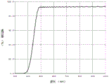
In order to verify that the blind holes 204 and the light-transmitting layer 1032 arranged in the OLED display panel 100 in the embodiment of the present application can realize the problem that light with a cut-off wavelength in a range of 370nm to 420nm normally passes through, that is, violet light can normally pass through, the applicant has performed two sets of experiments. As shown in fig. 3, one set of experiments was a conventional OLED display panel 200, and another was the OLED display panel 100 of the present application. The thickness and material of the conventional OLED display panel 200 are the same as those of the corresponding film layer of the OLED display panel 100, the thickness of the silicon nitride layer in the buffer layer 105 is 50nm, the thickness of the silicon dioxide layer is 300nm, the thickness of the first gate insulating layer 1061 is 130nm, the material is silicon dioxide, the thickness of the second gate insulating layer 1063 is 110nm, the material is silicon nitride, the thickness of the first interlayer insulating layer 1091 is 300nm, the material is silicon dioxide, the thickness of the first interlayer insulating layer 1094 is 200nm, the material is silicon nitride, the thickness of the planarization layer 201 is 1500nm, and the thickness of the pixel defining layer is 1500 nm. In the conventional OLED display panel 200, the first flexible layer is 6 μm thick and made of yellow polyimide, the first water blocking layer is 500nm thick and made of silicon dioxide, the second flexible layer is 6 μm thick and made of yellow polyimide, and the second water blocking layer is 500nm thick and made of silicon dioxide; in the OLED display panel 100 of the present application, the thickness of the first flexible layer 1033 is 6 μm, the material is transparent polyimide, the thickness of the first water blocking layer 1034 is 500nm, the material is silicon dioxide, the thickness of the second flexible layer 1035 is 6 μm, the material is transparent polyimide, the thickness of the second water blocking layer 1036 is 500nm, and the material is silicon dioxide. The results of the two sets of tests were measured with the same camera area under the same illumination, as shown in fig. 4 and 5.
Through comparison between fig. 4 and fig. 5, the OLED of the present application provides an OLED display panel 100, the average transmittance of the camera area is 30% to 80% due to the blind holes and the light transmission layer, the cutoff wavelength is 370nm to 420nm, and the wavelength of the violet light is 380 nm to 450nm, i.e., the violet light can normally transmit, the image pickup module below the display screen does not generate distortion during image pickup, and meanwhile, the average transmittance of the light in the image pickup area is improved, and the image pickup requirement under the visible light band screen is met.
According to the above OLED display panel, as shown in fig. 6, the present application further provides a display device 300, including: the above-mentioned OLED display panel; backplate 302, including the stiffening plate with be located the gum on stiffening plate surface, the gum is used for fixed OLED display panel 100, and the stiffening plate is preferred the aluminum alloy, and the thickness scope is 10 to 40um to it is die-cut to carry out the fluting to its surface, is favorable to OLED display panel 100 to dispel the heat. The camera assembly 3021 is located in the reinforcing plate, and the camera assembly 3021 is aligned with the blind hole 204 in the OLED display panel 100.
The invention has the beneficial effects that: according to the OLED display panel, the blind hole is formed between the drive circuit layer and the light-emitting functional layer, the light-transmitting layer is arranged on the position, corresponding to the blind hole, of the flexible substrate, the transparent polyimide is preferably made of transparent materials, when external light passes through the packaging layer and then passes through the blind hole and the light-transmitting layer, light with the cut-off wavelength of 370nm-420nm can normally pass through the light-transmitting layer, namely purple light can normally pass through the light-transmitting layer, a camera shooting assembly below the display screen cannot generate a distortion phenomenon during shooting, meanwhile, the average transmittance of light in a camera shooting area is improved, and the camera shooting requirement under a visible.
In summary, although the present invention has been described with reference to the preferred embodiments, the above-described preferred embodiments are not intended to limit the present invention, and those skilled in the art can make various changes and modifications without departing from the spirit and scope of the present invention, therefore, the scope of the present invention shall be determined by the appended claims.
Claims (10)
1. The OLED display panel is characterized by comprising a flexible substrate, a driving circuit layer, a light-emitting functional layer and an encapsulating layer, wherein the driving circuit layer, the light-emitting functional layer and the encapsulating layer are sequentially arranged on the flexible substrate in a laminated mode:
the light-emitting device comprises a driving circuit layer, a light-emitting functional layer, a packaging layer, a flexible substrate and a packaging layer, wherein a blind hole is formed between the driving circuit layer and the light-emitting functional layer, the packaging layer encapsulates the blind hole, a light-transmitting layer is arranged on the position, corresponding to the blind hole, of the flexible substrate, and the light-transmitting layer is provided with a light-.
2. The OLED display panel of claim 1, wherein the light transmissive material is a transparent polyimide.
3. The OLED display panel of claim 1, wherein the light transmissive layer comprises a glass substrate and a light transmissive material within the glass substrate.
4. The OLED display panel of claim 3, wherein the surface of the glass substrate is further provided with a hard coating, and the hard coating is made of silicon dioxide.
5. The OLED display panel of claim 1, wherein the blind holes are rectangular or trapezoidal in cross section.
6. The OLED display panel according to claim 1, wherein the blind hole penetrates through the driving circuit layer and a pixel defining layer in the light emitting function layer.
7. The OLED display panel of claim 1, wherein the insulating layer in the driving circuit layer is silicon oxide, silicon nitride or a highly light-transmissive organic material, wherein the insulating layer comprises a first gate insulating layer, a second gate insulating layer, a first interlayer insulating layer, a second interlayer insulating layer, and a planarization layer over the flexible substrate.
8. The OLED display panel of claim 7, wherein the insulating layer further has a plurality of cavities disposed therein.
9. The OLED display panel of claim 1, wherein the edge of the OLED display panel is further provided with a binding region, and the binding region is foldable to the back of the OLED display panel.
10. A display device, comprising:
the OLED display panel of any one of claims 1-9;
the back plate comprises a reinforcing plate and a back adhesive positioned on the surface of the reinforcing plate, and the back adhesive is used for fixing the OLED display panel;
and the camera shooting assembly is positioned in the reinforcing plate and is aligned with the blind hole in the OLED display panel.
Priority Applications (1)
| Application Number | Priority Date | Filing Date | Title |
|---|---|---|---|
| CN201911315145.XA CN111029385A (en) | 2019-12-19 | 2019-12-19 | OLED display panel and display device |
Applications Claiming Priority (1)
| Application Number | Priority Date | Filing Date | Title |
|---|---|---|---|
| CN201911315145.XA CN111029385A (en) | 2019-12-19 | 2019-12-19 | OLED display panel and display device |
Publications (1)
| Publication Number | Publication Date |
|---|---|
| CN111029385A true CN111029385A (en) | 2020-04-17 |
Family
ID=70209945
Family Applications (1)
| Application Number | Title | Priority Date | Filing Date |
|---|---|---|---|
| CN201911315145.XA Pending CN111029385A (en) | 2019-12-19 | 2019-12-19 | OLED display panel and display device |
Country Status (1)
| Country | Link |
|---|---|
| CN (1) | CN111029385A (en) |
Cited By (3)
| Publication number | Priority date | Publication date | Assignee | Title |
|---|---|---|---|---|
| CN113328046A (en) * | 2021-05-31 | 2021-08-31 | 武汉华星光电技术有限公司 | Display panel and preparation method thereof |
| CN113327961A (en) * | 2021-05-21 | 2021-08-31 | 武汉华星光电技术有限公司 | OLED display panel, preparation method thereof and OLED display device |
| CN116631285A (en) * | 2022-02-18 | 2023-08-22 | Uti有限公司 | Flexible hybrid cover window and method of making same |
Citations (5)
| Publication number | Priority date | Publication date | Assignee | Title |
|---|---|---|---|---|
| CN107680994A (en) * | 2017-10-30 | 2018-02-09 | 武汉华星光电半导体显示技术有限公司 | A kind of flexible OLED display panel and preparation method thereof |
| CN109671761A (en) * | 2018-12-19 | 2019-04-23 | 武汉华星光电半导体显示技术有限公司 | Display panel and preparation method thereof |
| CN110071121A (en) * | 2019-04-17 | 2019-07-30 | 武汉华星光电半导体显示技术有限公司 | Display panel and display device |
| CN110491910A (en) * | 2019-07-30 | 2019-11-22 | 武汉华星光电半导体显示技术有限公司 | A kind of display panel and preparation method thereof, display device |
| CN110556404A (en) * | 2019-08-09 | 2019-12-10 | 武汉华星光电半导体显示技术有限公司 | Display panel, manufacturing method thereof, and display device |
-
2019
- 2019-12-19 CN CN201911315145.XA patent/CN111029385A/en active Pending
Patent Citations (5)
| Publication number | Priority date | Publication date | Assignee | Title |
|---|---|---|---|---|
| CN107680994A (en) * | 2017-10-30 | 2018-02-09 | 武汉华星光电半导体显示技术有限公司 | A kind of flexible OLED display panel and preparation method thereof |
| CN109671761A (en) * | 2018-12-19 | 2019-04-23 | 武汉华星光电半导体显示技术有限公司 | Display panel and preparation method thereof |
| CN110071121A (en) * | 2019-04-17 | 2019-07-30 | 武汉华星光电半导体显示技术有限公司 | Display panel and display device |
| CN110491910A (en) * | 2019-07-30 | 2019-11-22 | 武汉华星光电半导体显示技术有限公司 | A kind of display panel and preparation method thereof, display device |
| CN110556404A (en) * | 2019-08-09 | 2019-12-10 | 武汉华星光电半导体显示技术有限公司 | Display panel, manufacturing method thereof, and display device |
Cited By (5)
| Publication number | Priority date | Publication date | Assignee | Title |
|---|---|---|---|---|
| CN113327961A (en) * | 2021-05-21 | 2021-08-31 | 武汉华星光电技术有限公司 | OLED display panel, preparation method thereof and OLED display device |
| WO2022241835A1 (en) * | 2021-05-21 | 2022-11-24 | 武汉华星光电技术有限公司 | Oled display panel and manufacturing method therefor, and oled display device |
| CN113328046A (en) * | 2021-05-31 | 2021-08-31 | 武汉华星光电技术有限公司 | Display panel and preparation method thereof |
| CN113328046B (en) * | 2021-05-31 | 2024-10-15 | 武汉华星光电技术有限公司 | Display panel and method for manufacturing the same |
| CN116631285A (en) * | 2022-02-18 | 2023-08-22 | Uti有限公司 | Flexible hybrid cover window and method of making same |
Similar Documents
| Publication | Publication Date | Title |
|---|---|---|
| KR102718638B1 (en) | Transparent organic light emitting display apparatus and method of manufacturing the same | |
| US10910441B2 (en) | Organic light emitting display device | |
| KR102910469B1 (en) | Display device | |
| KR102805657B1 (en) | Organic light emitting display | |
| CN111129270B (en) | Micro LED display device | |
| US11037995B2 (en) | Organic light-emitting display panel and display apparatus | |
| KR102745476B1 (en) | Display Device and Method for Manufacturing the Same | |
| KR102505255B1 (en) | Display apparatus | |
| KR20180047592A (en) | Organic light emitting display device amd nethod for manufacutring the same | |
| KR102583813B1 (en) | Display apparatus | |
| TWI628789B (en) | Display device and method of manufacturing same | |
| CN111326671B (en) | display device | |
| KR102900181B1 (en) | Display device | |
| CN111029385A (en) | OLED display panel and display device | |
| JP7418077B2 (en) | Semiconductor devices, display devices, and electronic equipment | |
| US12364072B2 (en) | Flexible double-sided display screen and manufacturing method thereof | |
| JP2018077982A (en) | Organic EL display device | |
| CN114512527A (en) | Display panel, manufacturing method thereof and display device | |
| CN108231833A (en) | Luminous display unit and its manufacturing method | |
| KR102787485B1 (en) | Organic light emitting display device | |
| CN114220821A (en) | display panel | |
| US20240357871A1 (en) | Display device and method of fabricating the same | |
| KR20150078392A (en) | Organic light emitting diode display device and fabricating method of the same | |
| KR20130073057A (en) | Organic light emitting diode display device and manufacturing method thereof | |
| EP4024492B1 (en) | Light-emitting device |
Legal Events
| Date | Code | Title | Description |
|---|---|---|---|
| PB01 | Publication | ||
| PB01 | Publication | ||
| SE01 | Entry into force of request for substantive examination | ||
| SE01 | Entry into force of request for substantive examination | ||
| RJ01 | Rejection of invention patent application after publication |
Application publication date: 20200417 |
|
| RJ01 | Rejection of invention patent application after publication |