CN110914981B - Semiconductor module - Google Patents
Semiconductor module Download PDFInfo
- Publication number
- CN110914981B CN110914981B CN201880001503.7A CN201880001503A CN110914981B CN 110914981 B CN110914981 B CN 110914981B CN 201880001503 A CN201880001503 A CN 201880001503A CN 110914981 B CN110914981 B CN 110914981B
- Authority
- CN
- China
- Prior art keywords
- die pad
- end surface
- frame
- semiconductor module
- electrode
- Prior art date
- Legal status (The legal status is an assumption and is not a legal conclusion. Google has not performed a legal analysis and makes no representation as to the accuracy of the status listed.)
- Active
Links
Images





Classifications
-
- H—ELECTRICITY
- H10—SEMICONDUCTOR DEVICES; ELECTRIC SOLID-STATE DEVICES NOT OTHERWISE PROVIDED FOR
- H10W—GENERIC PACKAGES, INTERCONNECTIONS, CONNECTORS OR OTHER CONSTRUCTIONAL DETAILS OF DEVICES COVERED BY CLASS H10
- H10W70/00—Package substrates; Interposers; Redistribution layers [RDL]
- H10W70/40—Leadframes
- H10W70/421—Shapes or dispositions
- H10W70/424—Cross-sectional shapes
- H10W70/427—Bent parts
-
- H—ELECTRICITY
- H10—SEMICONDUCTOR DEVICES; ELECTRIC SOLID-STATE DEVICES NOT OTHERWISE PROVIDED FOR
- H10W—GENERIC PACKAGES, INTERCONNECTIONS, CONNECTORS OR OTHER CONSTRUCTIONAL DETAILS OF DEVICES COVERED BY CLASS H10
- H10W70/00—Package substrates; Interposers; Redistribution layers [RDL]
- H10W70/40—Leadframes
- H10W70/411—Chip-supporting parts, e.g. die pads
- H10W70/415—Leadframe inner leads serving as die pads
-
- H—ELECTRICITY
- H10—SEMICONDUCTOR DEVICES; ELECTRIC SOLID-STATE DEVICES NOT OTHERWISE PROVIDED FOR
- H10W—GENERIC PACKAGES, INTERCONNECTIONS, CONNECTORS OR OTHER CONSTRUCTIONAL DETAILS OF DEVICES COVERED BY CLASS H10
- H10W70/00—Package substrates; Interposers; Redistribution layers [RDL]
- H10W70/40—Leadframes
- H10W70/421—Shapes or dispositions
- H10W70/424—Cross-sectional shapes
-
- H—ELECTRICITY
- H10—SEMICONDUCTOR DEVICES; ELECTRIC SOLID-STATE DEVICES NOT OTHERWISE PROVIDED FOR
- H10W—GENERIC PACKAGES, INTERCONNECTIONS, CONNECTORS OR OTHER CONSTRUCTIONAL DETAILS OF DEVICES COVERED BY CLASS H10
- H10W70/00—Package substrates; Interposers; Redistribution layers [RDL]
- H10W70/40—Leadframes
- H10W70/464—Additional interconnections in combination with leadframes
- H10W70/466—Tape carriers or flat leads
-
- H—ELECTRICITY
- H10—SEMICONDUCTOR DEVICES; ELECTRIC SOLID-STATE DEVICES NOT OTHERWISE PROVIDED FOR
- H10W—GENERIC PACKAGES, INTERCONNECTIONS, CONNECTORS OR OTHER CONSTRUCTIONAL DETAILS OF DEVICES COVERED BY CLASS H10
- H10W70/00—Package substrates; Interposers; Redistribution layers [RDL]
- H10W70/40—Leadframes
- H10W70/481—Leadframes for devices being provided for in groups H10D8/00 - H10D48/00
-
- H—ELECTRICITY
- H10—SEMICONDUCTOR DEVICES; ELECTRIC SOLID-STATE DEVICES NOT OTHERWISE PROVIDED FOR
- H10W—GENERIC PACKAGES, INTERCONNECTIONS, CONNECTORS OR OTHER CONSTRUCTIONAL DETAILS OF DEVICES COVERED BY CLASS H10
- H10W74/00—Encapsulations, e.g. protective coatings
- H10W74/10—Encapsulations, e.g. protective coatings characterised by their shape or disposition
- H10W74/111—Encapsulations, e.g. protective coatings characterised by their shape or disposition the semiconductor body being completely enclosed
-
- H—ELECTRICITY
- H10—SEMICONDUCTOR DEVICES; ELECTRIC SOLID-STATE DEVICES NOT OTHERWISE PROVIDED FOR
- H10W—GENERIC PACKAGES, INTERCONNECTIONS, CONNECTORS OR OTHER CONSTRUCTIONAL DETAILS OF DEVICES COVERED BY CLASS H10
- H10W72/00—Interconnections or connectors in packages
- H10W72/071—Connecting or disconnecting
- H10W72/073—Connecting or disconnecting of die-attach connectors
- H10W72/07351—Connecting or disconnecting of die-attach connectors characterised by changes in properties of the die-attach connectors during connecting
-
- H—ELECTRICITY
- H10—SEMICONDUCTOR DEVICES; ELECTRIC SOLID-STATE DEVICES NOT OTHERWISE PROVIDED FOR
- H10W—GENERIC PACKAGES, INTERCONNECTIONS, CONNECTORS OR OTHER CONSTRUCTIONAL DETAILS OF DEVICES COVERED BY CLASS H10
- H10W72/00—Interconnections or connectors in packages
- H10W72/071—Connecting or disconnecting
- H10W72/073—Connecting or disconnecting of die-attach connectors
- H10W72/07351—Connecting or disconnecting of die-attach connectors characterised by changes in properties of the die-attach connectors during connecting
- H10W72/07354—Connecting or disconnecting of die-attach connectors characterised by changes in properties of the die-attach connectors during connecting changes in dispositions
-
- H—ELECTRICITY
- H10—SEMICONDUCTOR DEVICES; ELECTRIC SOLID-STATE DEVICES NOT OTHERWISE PROVIDED FOR
- H10W—GENERIC PACKAGES, INTERCONNECTIONS, CONNECTORS OR OTHER CONSTRUCTIONAL DETAILS OF DEVICES COVERED BY CLASS H10
- H10W72/00—Interconnections or connectors in packages
- H10W72/30—Die-attach connectors
-
- H—ELECTRICITY
- H10—SEMICONDUCTOR DEVICES; ELECTRIC SOLID-STATE DEVICES NOT OTHERWISE PROVIDED FOR
- H10W—GENERIC PACKAGES, INTERCONNECTIONS, CONNECTORS OR OTHER CONSTRUCTIONAL DETAILS OF DEVICES COVERED BY CLASS H10
- H10W72/00—Interconnections or connectors in packages
- H10W72/30—Die-attach connectors
- H10W72/341—Dispositions of die-attach connectors, e.g. layouts
- H10W72/347—Dispositions of multiple die-attach connectors
-
- H—ELECTRICITY
- H10—SEMICONDUCTOR DEVICES; ELECTRIC SOLID-STATE DEVICES NOT OTHERWISE PROVIDED FOR
- H10W—GENERIC PACKAGES, INTERCONNECTIONS, CONNECTORS OR OTHER CONSTRUCTIONAL DETAILS OF DEVICES COVERED BY CLASS H10
- H10W72/00—Interconnections or connectors in packages
- H10W72/90—Bond pads, in general
- H10W72/921—Structures or relative sizes of bond pads
- H10W72/926—Multiple bond pads having different sizes
-
- H—ELECTRICITY
- H10—SEMICONDUCTOR DEVICES; ELECTRIC SOLID-STATE DEVICES NOT OTHERWISE PROVIDED FOR
- H10W—GENERIC PACKAGES, INTERCONNECTIONS, CONNECTORS OR OTHER CONSTRUCTIONAL DETAILS OF DEVICES COVERED BY CLASS H10
- H10W74/00—Encapsulations, e.g. protective coatings
-
- H—ELECTRICITY
- H10—SEMICONDUCTOR DEVICES; ELECTRIC SOLID-STATE DEVICES NOT OTHERWISE PROVIDED FOR
- H10W—GENERIC PACKAGES, INTERCONNECTIONS, CONNECTORS OR OTHER CONSTRUCTIONAL DETAILS OF DEVICES COVERED BY CLASS H10
- H10W90/00—Package configurations
- H10W90/701—Package configurations characterised by the relative positions of pads or connectors relative to package parts
- H10W90/731—Package configurations characterised by the relative positions of pads or connectors relative to package parts of die-attach connectors
- H10W90/736—Package configurations characterised by the relative positions of pads or connectors relative to package parts of die-attach connectors between a chip and a stacked lead frame, conducting package substrate or heat sink
Landscapes
- Structures Or Materials For Encapsulating Or Coating Semiconductor Devices Or Solid State Devices (AREA)
Abstract
本发明涉及的半导体模块,包括:裸片焊盘框(DF);半导体芯片(CX);裸片焊盘用导电性连接构件(A2);以及封装树脂(H),其中,所述裸片焊盘框具有:突起部(T),配置在所述裸片焊盘框的主体(B)的端部(Ba)的上侧并且从所述裸片焊盘框的所述主体的上端面向与所述裸片焊盘框的所述主体的上端面相平行的方向延伸,用于提高与所述封装树脂之间的密合性,在所述突起部的前端,设置有部分位于比所述突起部的上端面更上方的锁紧部(U)。

A semiconductor module according to the present invention includes: a die pad frame (DF); a semiconductor chip (CX); a conductive connection member (A2) for a die pad; and an encapsulation resin (H), wherein the die The pad frame has a protrusion (T) arranged on the upper side of the end (Ba) of the main body (B) of the die pad frame and facing from the upper end of the main body of the die pad frame Extending in a direction parallel to the upper end surface of the main body of the die pad frame to improve the adhesion with the encapsulation resin, at the front end of the protrusion, a portion located The locking part (U) above the upper end surface of the protrusion.
Description
技术领域technical field
本发明涉及一种半导体模块。The invention relates to a semiconductor module.
背景技术Background technique
以往,有一种半导体模块已被普遍认知,其具备:半导体芯片;通过键合线与该半导体芯片电连接的引线框;用于封装半导体芯片与引线框的封装树脂;以及利用接合材料接合在半导体芯片上的裸片焊盘框(die-pad frame)(例如参照特开平06-260572,特开2008-311366等)。In the past, a semiconductor module has been generally known, which has: a semiconductor chip; a lead frame electrically connected to the semiconductor chip through a bonding wire; an encapsulating resin for encapsulating the semiconductor chip and the lead frame; A die-pad frame on a semiconductor chip (see, for example, JP-A-06-260572, JP-A-2008-311366, etc.).
这种半导体模块通过在裸片焊盘框的端部设置突起部,从而来提升封装树脂与该裸片焊盘框之间的密合性。Such a semiconductor module improves the adhesion between the encapsulating resin and the die pad frame by providing a protrusion at the end of the die pad frame.
然而,在这种半导体模块上,用于配置半导体芯片的裸片焊盘框DF的端部处有时会发生封装树脂H产生裂痕K或剥离的问题(图14、图15)。However, in such a semiconductor module, cracks K or peeling of the encapsulating resin H sometimes occur at the end of the die pad frame DF for arranging the semiconductor chip ( FIGS. 14 and 15 ).
因此,本发明的目的,是提供一种半导体模块,其能够在裸片焊盘框的端部附近一边抑制将半导体芯片与裸片焊盘框电连接的导电性连接构件的流动,一边抑制裸片焊盘框端部处产生的封装树脂的开裂和剥离。Therefore, it is an object of the present invention to provide a semiconductor module capable of suppressing the flow of a conductive connection member electrically connecting a semiconductor chip and a die pad frame near the end of the die pad frame and suppressing the flow of the die pad frame. Cracking and peeling of the encapsulating resin at the end of the die pad frame.
发明内容Contents of the invention
本发明的一种形态涉及的半导体模块,其特征在于,包括:A semiconductor module according to an aspect of the present invention is characterized by comprising:
裸片焊盘框;die pad frame;
半导体芯片,配置在所述裸片焊盘框的上端面上的芯片区域上,并且上端面配置有第一电极,下端面配置有第二电极;A semiconductor chip is arranged on the chip area on the upper end surface of the die pad frame, and the upper end surface is provided with a first electrode, and the lower end surface is provided with a second electrode;
裸片焊盘用导电性连接构件,位于所述半导体芯片的所述第二电极与所述裸片焊盘框的上端面之间,用于将所述半导体芯片的所述第二电极与所述裸片焊盘框的上端面电连接;以及a conductive connection member for a die pad, located between the second electrode of the semiconductor chip and the upper end surface of the die pad frame, for connecting the second electrode of the semiconductor chip to the electrical connection to the upper surface of the die pad frame; and
封装树脂,用于封装所述半导体芯片、所述裸片焊盘框、以及所述裸片焊盘用导电性连接构件,an encapsulating resin for encapsulating the semiconductor chip, the die pad frame, and the conductive connection member for the die pad,
其中,所述裸片焊盘框具有:wherein the die pad frame has:
突起部,配置在所述裸片焊盘框的主体的端部的上侧并且从所述裸片焊盘框的所述主体的上端面向与所述裸片焊盘框的所述主体的上端面相平行的方向延伸,用于提高与所述封装树脂之间的密合性,a protrusion disposed on an upper side of an end portion of the main body of the die pad frame and facing from the upper end of the main body of the die pad frame to the upper end of the main body of the die pad frame The planes extend in a direction parallel to improve the adhesion with the encapsulation resin,
在所述突起部的前端,设置有部分位于比所述突起部的上端面更上方的锁紧部。At the front end of the protruding part, there is provided a locking part partially located above the upper end surface of the protruding part.
在所述半导体模块中,进一步包括:In the semiconductor module, further comprising:
第一线夹框,配置在所述半导体芯片的上端面上;以及a first wire clip frame configured on the upper surface of the semiconductor chip; and
第一线夹用导电性连接部件,位于所述半导体芯片的所述第一电极与所述第一线夹框的下端面之间,用于将所述半导体芯片的所述第一电极与所述第一线夹框的下端面电连接。The conductive connecting member for the first wire clamp is located between the first electrode of the semiconductor chip and the lower end surface of the first wire clamp frame, and is used to connect the first electrode of the semiconductor chip to the lower end surface of the first wire clamp frame. The lower end surface of the first wire clip frame is electrically connected.
在所述半导体模块中,In the semiconductor module,
所述锁紧部具有从所述突起部的前端的上端面向上方突出的段差。The locking portion has a step protruding upward from the upper end surface of the front end of the protruding portion.
在所述半导体模块中,In the semiconductor module,
所述锁紧部具有从所述突起部的前端的上端面向上方呈阶段性突出的多个段差。The locking portion has a plurality of stepwise protruding upwards from the upper end surface of the front end of the protruding portion.
在所述半导体模块中,In the semiconductor module,
所述锁紧部的上部的高度比所述裸片焊盘用导电性连接构件的上部的高度更高,从而用于封堵所述裸片焊盘用导电性连接构件的流动。An upper portion of the locking portion is higher in height than an upper portion of the conductive connection member for die pads, thereby blocking a flow of the conductive connection member for die pads.
在所述半导体模块中,In the semiconductor module,
在所述突起部延伸的所述方向上,所述锁紧部的长度比所述突起部中除所述锁紧部以外部分的长度更短。In the direction in which the protrusion extends, the length of the locking portion is shorter than the length of a portion of the protrusion other than the locking portion.
在所述半导体模块中,In the semiconductor module,
所述突起部沿所述裸片焊盘框的所述主体的上端面的端部周围连续地配置。The protruding portion is continuously arranged around an end portion of the upper end surface of the main body of the die pad frame.
在所述半导体模块中,In the semiconductor module,
所述锁紧部的端部为矩形或弯曲的形状。The end of the locking part is rectangular or curved.
在所述半导体模块中,In the semiconductor module,
所述锁紧部是通过将所述突起部的前端向上方按压后形成的。The locking portion is formed by pressing the front end of the protruding portion upward.
在所述半导体模块中,In the semiconductor module,
所述封装树脂的线膨胀系数小于所述裸片焊盘框的线膨胀系数,并且,大于所述半导体芯片的线膨胀系数。The linear expansion coefficient of the encapsulation resin is smaller than that of the die pad frame, and larger than that of the semiconductor chip.
在所述半导体模块中,In the semiconductor module,
所述锁紧部是通过将所述突起部的前端向上方进行多次按压后形成的。The locking portion is formed by pressing the front end of the protruding portion upwards several times.
在所述半导体模块中,In the semiconductor module,
所述半导体芯片的上端面上配置有上端面的面积比所述第一电极更小的第三电极。A third electrode having a smaller upper end surface area than the first electrode is disposed on the upper end surface of the semiconductor chip.
在所述半导体模块中,进一步包括:In the semiconductor module, further comprising:
第二线夹框,在所述半导体芯片的上端面上与所述第一线夹框邻接配置,并且上端面的面积比所述第一线夹框更小;以及The second wire clamp frame is arranged adjacent to the first wire clamp frame on the upper end surface of the semiconductor chip, and the area of the upper end surface is smaller than that of the first wire clamp frame; and
第二线夹用导电性连接部件,用于将所述半导体芯片的所述第三电极与所述第二线夹框的下端面电连接。The conductive connecting member for the second wire clip is used to electrically connect the third electrode of the semiconductor chip with the lower end surface of the second wire clip frame.
在所述半导体模块中,In the semiconductor module,
所述第一线夹用导电性连接部件、第二线夹用导电性连接部件、以及裸片焊盘用导电性连接构件均为焊锡构件。The conductive connecting member for the first clip, the conductive connecting member for the second clip, and the conductive connecting member for the die pad are all solder members.
在所述半导体模块中,In the semiconductor module,
所述半导体芯片为MOS晶体管,The semiconductor chip is a MOS transistor,
所述第一电极为所述MOS晶体管的源电极,The first electrode is the source electrode of the MOS transistor,
所述第二电极为所述MOS晶体管的漏电极,The second electrode is the drain electrode of the MOS transistor,
所述第三电极为所述MOS晶体管的栅电极。The third electrode is the gate electrode of the MOS transistor.
在所述半导体模块中,In the semiconductor module,
所述裸片焊盘框的所述突起部上设置有通过激光照射形成的一个或多个激光槽,从而使一个或多个所述激光槽在所述突起部的上端面上沿所述裸片焊盘框的所述主体的端部延伸。The protruding portion of the die pad frame is provided with one or more laser grooves formed by laser irradiation, so that the one or more laser grooves are formed on the upper end surface of the protruding portion along the die The ends of the main body of the chip pad frame extend.
在所述半导体模块中,In the semiconductor module,
与所述突起部的上端面上的所述激光槽所延伸的长度方向相垂直的所述激光槽的截面形状呈V字形或U字形,The cross-sectional shape of the laser groove perpendicular to the length direction in which the laser groove extends on the upper end surface of the protrusion is V-shaped or U-shaped,
所述激光槽中的第一激光槽的底部比所述第一激光槽的宽度的中心更偏向配置有所述半导体芯片的芯片区域一侧。A bottom of a first laser groove among the laser grooves is more offset from a center of a width of the first laser groove toward a chip region where the semiconductor chip is arranged.
在所述半导体模块中,In the semiconductor module,
相对于所述突起部的上端面上形成有所述第一激光槽的槽区域的所述激光照射的方向,从穿过所述突起部的上端面上的所述槽区域的垂直线向所述锁紧部一侧倾斜。From a vertical line passing through the groove region on the upper end surface of the protrusion to the One side of the locking part is inclined.
在所述半导体模块中,In the semiconductor module,
所述突起部的上端面上的与所述激光槽所延伸的长度方向相垂直的所述激光槽的截面形状呈V字形或U字形,The cross-sectional shape of the laser groove perpendicular to the length direction in which the laser groove extends on the upper end surface of the protrusion is V-shaped or U-shaped,
所述激光槽中的第二激光槽的底部比所述第二激光槽的宽度的中心更偏向所述锁紧部一侧。The bottom of the second laser groove among the laser grooves is more inclined to the side of the locking part than the center of the width of the second laser groove.
在所述半导体模块中,In the semiconductor module,
相对于所述突起部的上端面上形成有所述第二激光槽的槽区域的所述激光照射的方向,从穿过所述突起部的上端面上的所述槽区域的垂直线向配置有所述半导体芯片的芯片区域一侧倾斜。Arranged from a vertical line passing through the groove region on the upper end surface of the protrusion with respect to the laser irradiation direction of the groove region in which the second laser groove is formed on the upper end surface of the protrusion One side of the chip area with the semiconductor chip is inclined.
在所述半导体模块中,In the semiconductor module,
通过所述激光照射,所述激光槽的内端面以及所述激光槽的边缘部被粗糙化,从而在所述裸片焊盘框的上端面上抑制所述裸片焊盘用导电性连接构件的流动扩展。The inner end surface of the laser groove and the edge portion of the laser groove are roughened by the laser irradiation, thereby suppressing the conductive connection member for die pad on the upper end surface of the die pad frame. flow extension.
在所述半导体模块中,In the semiconductor module,
所述裸片焊盘框具有:第一边、一端与所述第一边相交的第二边、一端与所述第一边的另一端相交的第三边、以及一端与所述第二边的另一端相交且另一端与所述第三边相交的第四边,The die pad frame has a first side, a second side having one end intersecting the first side, a third side having one end intersecting the other end of the first side, and a second side intersecting one end with the second side. the fourth side that intersects the other end of and intersects the third side at the other end,
所述突起部以及所述锁紧部被形成在沿第一、第二、以及第三边的区域上,并且,未被形成在沿所述第四边的区域上,The protrusion and the locking portion are formed on regions along the first, second, and third sides, and are not formed on regions along the fourth side,
在所述裸片焊盘框的上端面上的沿所述第四边的所述区域上,形成有贯穿所述主体的,并且用于提升与所述封装树脂之间的密合性的贯穿孔,On the region along the fourth side on the upper end surface of the die pad frame, a penetrating hole for improving the adhesion with the encapsulation resin is formed that penetrates the main body. hole,
在所述突起部的上端面上,设置有通过所述激光照射形成的所述激光槽,从而使所述激光槽沿所述裸片焊盘框的所述第一、第二、以及第三边延伸,On the upper end surface of the protruding portion, the laser groove formed by the laser irradiation is provided, so that the laser groove is formed along the first, second, and third sides of the die pad frame. side extension,
沿所述第四边,在形成有所述贯穿孔的所述区域与所述芯片区域之间,设置有通过激光照射形成的一个或多个追加激光槽。Along the fourth side, one or more additional laser grooves formed by laser irradiation are provided between the region where the through hole is formed and the chip region.
在所述半导体模块中,In the semiconductor module,
所述激光槽沿所述裸片焊盘框的所述第一、第二、以及第三边连续形成,the laser slots are formed continuously along the first, second, and third sides of the die pad frame,
所述追加激光槽的数量多于所述激光槽的数量。The number of the additional laser grooves is greater than the number of the laser grooves.
在所述半导体模块中,In the semiconductor module,
所述激光槽与所述追加激光槽相连通,并且将配置有所述半导体芯片的所述裸片焊盘框的芯片区域的外周包围。The laser groove communicates with the additional laser groove, and surrounds an outer periphery of a chip area of the die pad frame where the semiconductor chip is disposed.
在所述半导体模块中,In the semiconductor module,
构成所述裸片焊盘框的导电性金属材料为:铜材、或在铜材中添加了Sn、Zn、Fe、Cr、Ni中的任意一种异种金属后的合金,所述裸片焊盘框的表面未经过电镀处理。The conductive metal material constituting the die pad frame is: copper, or an alloy in which any one of dissimilar metals among Sn, Zn, Fe, Cr, and Ni is added to the copper material, and the die soldering The surface of the disk frame is not electroplated.
在所述半导体模块中,In the semiconductor module,
所述锁紧部的下端面与所述突起部的下端面之间的段差的高度大于所述锁紧部的上端面与所述突起部的上端面之间的段差的高度。The height of the step difference between the lower end surface of the locking part and the lower end surface of the protrusion is greater than the height of the step difference between the upper end surface of the locking part and the upper end surface of the protrusion.
在所述半导体模块中,In the semiconductor module,
所述锁紧部的下端面向着所述锁紧部的端部朝上方倾斜。The lower end of the locking portion is inclined upward toward the end of the locking portion.
在所述半导体模块中,In the semiconductor module,
在所述第一线夹框的上端面的端部,设置有部分位于比所述第一线夹框的上端面更上方的线夹用锁紧部,从而使所述线夹用锁紧部与所述半导体芯片的上端面分离,At the end of the upper end surface of the first wire clamp frame, a locking portion for wire clamps partially located above the upper end surface of the first wire clamp frame is provided, so that the locking portion for wire clamps separated from the upper surface of the semiconductor chip,
所述线夹用锁紧部的下端面向着所述线夹用锁紧部的端部朝上方倾斜。A lower end surface of the locking portion for wire clips is inclined upward toward an end portion of the locking portion for wire clips.
在所述半导体模块中,In the semiconductor module,
所述线夹用锁紧部的上端面向着所述线夹用锁紧部的端部朝下方倾斜。The upper end surface of the locking part for wire clips is inclined downward toward the end of the locking part for wire clips.
在所述半导体模块中,In the semiconductor module,
与所述锁紧部的下端面相连的所述突起部的下端面的端部呈弯曲的形状。The end portion of the lower end surface of the protrusion connected to the lower end surface of the locking portion is in a curved shape.
在所述半导体模块中,In the semiconductor module,
所述锁紧部的下端面的端部呈弯曲的形状。The end portion of the lower end surface of the locking portion is in a curved shape.
发明效果Invention effect
本发明的一种形态涉及的半导体模块,包括:裸片焊盘框;半导体芯片,配置在裸片焊盘框的上端面上的芯片区域上,并且上端面配置有第一电极,下端面配置有第二电极;裸片焊盘用导电性连接构件,位于半导体芯片的第二电极与裸片焊盘框的上端面之间,用于将半导体芯片的第二电极与裸片焊盘框的上端面电连接;以及封装树脂,用于封装半导体芯片、裸片焊盘框、以及裸片焊盘用导电性连接构件。A semiconductor module according to an aspect of the present invention includes: a die pad frame; a semiconductor chip disposed on a chip region on an upper end surface of the die pad frame, and a first electrode is disposed on the upper end surface, and a semiconductor chip is disposed on the lower end surface. There is a second electrode; the conductive connection member for the die pad is located between the second electrode of the semiconductor chip and the upper end surface of the die pad frame, and is used to connect the second electrode of the semiconductor chip to the die pad frame an upper end face electrical connection; and an encapsulation resin for encapsulating the semiconductor chip, the die pad frame, and the conductive connection member for the die pad.
并且,裸片焊盘框具有:突起部,配置在裸片焊盘框的主体的端部的上侧并且从裸片焊盘框的主体的上端面向与裸片焊盘框的主体的上端面相平行的方向延伸,用于提高与封装树脂之间的密合性,并且,在突起部的前端,设置有部分位于比突起部的上端面更上方的锁紧部。And, the die pad frame has: a protruding part arranged on the upper side of the end part of the main body of the die pad frame and facing from the upper end face of the main body of the die pad frame to the upper end surface of the main body of the die pad frame. Extending in a parallel direction is used to improve the adhesiveness with the encapsulation resin, and a locking portion partially located above the upper end surface of the protrusion is provided at the front end of the protrusion.
通过这样,裸片焊盘框的突起部的前端的锁紧部就能够对裸片焊盘用导电性连接构件进行封堵。In this way, the locking portion at the tip of the protruding portion of the die pad frame can seal the die pad conductive connection member.
再有,在裸片焊盘框的突起部的前端附近,通过利用该锁紧部来对封装树脂的收缩进行抑制,就能够抑制该封装树脂产生的开裂和剥离。Furthermore, by suppressing shrinkage of the encapsulating resin by the locking portion in the vicinity of the front end of the protruding portion of the die pad frame, cracking and peeling of the encapsulating resin can be suppressed.
如上述般,根据本发明的半导体模块,就能够在裸片焊盘框的端部附近一边抑制将半导体芯片与裸片焊盘框电连接的导电性连接构件的流动,一边抑制裸片焊盘框端部处产生的封装树脂的开裂和剥离。As described above, according to the semiconductor module of the present invention, it is possible to suppress the flow of the conductive connection member electrically connecting the semiconductor chip and the die pad frame near the end portion of the die pad frame while suppressing the flow of the die pad. Cracking and peeling of the encapsulating resin generated at the end of the frame.
附图说明Description of drawings
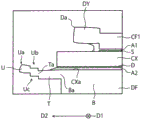
图1是展示实施例一涉及的半导体模块100的一例外观构成的上端面图。FIG. 1 is an upper end view showing an example of the external configuration of a
图2是展示图1所示的半导体模块100的一例外观构成的下端面图。FIG. 2 is a bottom view showing an example of the external configuration of the
图3是展示图1所示的半导体模块100的一例外观构成的,从第一方向D1的相反一侧进行观后后的侧面图。FIG. 3 is a side view showing an example of the external configuration of the
图4是展示图1所示的半导体模块100的一例外观构成的,从第二方向D2进行观后后的侧面图。FIG. 4 is a side view showing an example of the external configuration of the
图5是展示图1所示的半导体模块100的一例外观构成的,从第一方向D1进行观后后的侧面图。FIG. 5 is a side view showing an example of the external configuration of the
图6是展示实施例一涉及的半导体模块100的一例内部构成的上端面图。FIG. 6 is a top view showing an example of the internal structure of the
图7是展示沿图6所示的半导体模块的N-N线切割后的截面的一例截面图。FIG. 7 is a cross-sectional view showing an example of a cross section cut along the N-N line of the semiconductor module shown in FIG. 6 .
图8是展示沿图6所示的半导体模块的N-N线切割后的截面的另一例截面图。FIG. 8 is another cross-sectional view showing a cross-section cut along the N-N line of the semiconductor module shown in FIG. 6 .
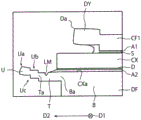
图9是展示实施例二涉及的半导体模块的截面的一例截面图。9 is a cross-sectional view showing an example of a cross-section of a semiconductor module according to the second embodiment.
图10是展示实施例二涉及的半导体模块的截面的另一例截面图。10 is another cross-sectional view showing a cross-section of the semiconductor module according to the second embodiment.
图11是展示实施例二涉及的半导体模块的裸片焊盘框DF的上端面构成的一例上端面图。FIG. 11 is an upper end view showing an example of the upper end configuration of the die pad frame DF of the semiconductor module according to the second embodiment.
图12是展示通过激光照射在裸片焊盘框DF的突起部T上形成激光槽LM的一例工序的裸片焊盘框DF截面图。12 is a sectional view of the die pad frame DF showing an example of a process of forming laser grooves LM on the protrusion T of the die pad frame DF by laser irradiation.
图13是展示通过激光照射在裸片焊盘框DF的突起部T上形成第一、第二激光槽LMa、LMb的一例工序的裸片焊盘框DF截面图。13 is a sectional view of the die pad frame DF showing an example of a process of forming first and second laser grooves LMa, LMb on the protrusion T of the die pad frame DF by laser irradiation.
图14是展示以往的半导体模块构成的一例下端面图。FIG. 14 is a bottom view showing an example of the structure of a conventional semiconductor module.
图15是展示沿图14中所示的以往的半导体模块的N-N线进行切割后的一例截面图。FIG. 15 is a cross-sectional view showing an example of cutting along the N-N line of the conventional semiconductor module shown in FIG. 14 .
具体实施方式Detailed ways
以下,将参照附图对本发明涉及的实施方式进行说明。Hereinafter, embodiments according to the present invention will be described with reference to the drawings.
【实施例一】[Example 1]
图1是展示实施例一涉及的半导体模块100的一例外观构成的上端面图。图2是展示图1所示的半导体模块100的一例外观构成的下端面图。图3是展示图1所示的半导体模块100的一例外观构成的,从第一方向D1的相反一侧进行观后后的侧面图。图4是展示图1所示的半导体模块100的一例外观构成的,从第二方向D2进行观后后的侧面图。图5是展示图1所示的半导体模块100的一例外观构成的,从第一方向D1进行观后后的侧面图。图6是展示实施例一涉及的半导体模块100的一例内部构成的上端面图。图7是展示沿图6所示的半导体模块的N-N线切割后的截面的一例截面图。图8是展示沿图6所示的半导体模块的N-N线切割后的截面的另一例截面图。另外,在图6中,对封装构件A做了透明化处理。FIG. 1 is an upper end view showing an example of the external configuration of a
例如图1至图8所示,实施例一涉及的半导体模块100包括:裸片焊盘框(引线框)DF、半导体芯片CX、裸片焊盘用导电性连接构件A2、封装树脂H、第一线夹框CF1、第一线夹用导电性连接构件A1、第二线夹框CF2、以及第二线夹用导电性连接构件A3。For example, as shown in FIGS. 1 to 8 , the
在本实施例中,半导体模块100是作为三端子的半导体装置(MOS晶体管)来发挥功能的。In this embodiment, the
并且,半导体芯片CX被配置在裸片焊盘框DF的上端面上的芯片区域CXa上。Furthermore, the semiconductor chip CX is arranged on the chip region CXa on the upper end surface of the die pad frame DF.
该半导体芯片CX的上端面上设置有第一电极(源电极)S,下端面上设置有第二电极(漏电极)D。该半导体芯片CX的上端面上还设置有上端面的面积小于第一电极S的第三电极(栅电极)G。The semiconductor chip CX has a first electrode (source electrode) S provided on the upper end surface, and a second electrode (drain electrode) D provided on the lower end surface. A third electrode (gate electrode) G whose upper end surface area is smaller than that of the first electrode S is also provided on the upper end surface of the semiconductor chip CX.
该半导体芯片CX在本实施例中例如为MOS晶体管。此情况下,第一电极S为该MOS晶体管的源电极,第二电极D为该MOS晶体管的漏电极,第三电极G为该MOS晶体管的栅电极。This semiconductor chip CX is, for example, a MOS transistor in this embodiment. In this case, the first electrode S is the source electrode of the MOS transistor, the second electrode D is the drain electrode of the MOS transistor, and the third electrode G is the gate electrode of the MOS transistor.
另外,裸片焊盘用导电性连接构件A2位于半导体芯片CX的第二电极D与裸片焊盘框DF的上端面之间。Moreover, the electroconductive connection member A2 for die pads is located between the 2nd electrode D of the semiconductor chip CX, and the upper end surface of the die pad frame DF.
该裸片焊盘用导电性连接构件A2将半导体芯片CX的第二电极D与裸片焊盘框DF的上端面电连接。The die pad conductive connection member A2 electrically connects the second electrode D of the semiconductor chip CX and the upper end surface of the die pad frame DF.
该裸片焊盘用导电性连接构件A2例如为焊锡构件。This conductive connection member A2 for die pads is a solder member, for example.
第一线夹框CF1例如图6以及图7所示,配置在半导体芯片CX的上端面上。For example, as shown in FIGS. 6 and 7 , the first clip frame CF1 is disposed on the upper end surface of the semiconductor chip CX.
该第一线夹框CF1例如图1至图6所示,具有从封装树脂H突出的端子CF1a、CF1b、CF1c。This first clamp frame CF1 has terminals CF1a, CF1b, and CF1c protruding from the encapsulating resin H, for example, as shown in FIGS. 1 to 6 .
第一线夹框CF1的上端面的端部,设置有部分位于比第一线夹框CF1的上端面更上方的线夹用锁紧部DY,从而使线夹用锁紧部DY与半导体芯片CX的上端面分离。该线夹用锁紧部DY的端部Da呈矩形或弯曲形。The end portion of the upper end surface of the first wire clamp frame CF1 is provided with a wire clamp locking portion DY that is partially located above the upper end surface of the first wire clamp frame CF1, so that the wire clamp lock portion DY is connected to the semiconductor chip. The upper end surface of CX is separated. The end Da of the clamp DY is rectangular or curved.
通过该线夹用锁紧部DY,第一线夹框CF1的端部附近的封装树脂H就被模塑固定(Mold lock)。The sealing resin H in the vicinity of the end of the first clamp frame CF1 is molded and fixed by the clamp DY.
另外,第一线夹框CF1例如图6所示,具有通过从上方按压后向下方突出的四个凸部CF1D。该四个凸部CF1D例如直接地过通过第一线夹用导电性连接构件A1与半导体芯片CX的第一电极(源电极)S相接触。Moreover, as shown in FIG. 6, for example, 1st wire clamp frame CF1 has four convex parts CF1D protruding downward after being pressed from above. The four protrusions CF1D are in direct contact with the first electrode (source electrode) S of the semiconductor chip CX, for example, via the first conductive connection member A1 for a clip.
第一线夹用导电性连接构件A1例如图7、图8所示,位于半导体芯片CX的第一电极S与第一线夹框CF1的下端面之间。For example, as shown in FIG. 7 and FIG. 8 , the first conductive connection member A1 for wire clamp is located between the first electrode S of the semiconductor chip CX and the lower end surface of the first wire clamp frame CF1 .
该第一线夹用导电性连接构件A1将半导体芯片CX的第一电极S与第一线夹框CF1的下端面电连接。The first clamp conductive connection member A1 electrically connects the first electrode S of the semiconductor chip CX to the lower end surface of the first clamp frame CF1.
该第一线夹用导电性连接构件A1例如为焊锡构件。The first conductive connection member A1 for clips is, for example, a solder member.
第二线夹框CF2在半导体芯片CX的山端面上与第一线夹框CF1相邻配置。The second lead frame CF2 is arranged adjacent to the first lead frame CF1 on the mountain end surface of the semiconductor chip CX.
该第二线夹框CF2具有从封装树脂H突出的端子CF2a。This second clamp frame CF2 has a terminal CF2a protruding from the encapsulating resin H. As shown in FIG.
该第二线夹框CF2的上端面的面积比第一线夹框CF1更小。The area of the upper end surface of the second wire clamping frame CF2 is smaller than that of the first wire clamping frame CF1.
第二线夹用导电性连接构件A3将半导体芯片CX的第三电极G与第二线夹框CF2的下端面电连接。The second clamp conductive connection member A3 electrically connects the third electrode G of the semiconductor chip CX and the lower end surface of the second clamp frame CF2.
该第二线夹用导电性连接构件A3例如为焊锡构件。The second conductive connection member A3 for clamps is, for example, a solder member.
封装树脂H用于封装:半导体芯片CX、裸片焊盘框DF、第一线夹框CF1、第一线夹用导电性连接构件A1、第二线夹框CF2、第二线夹用导电性连接构件A3、以及裸片焊盘用导电性连接构件A2。Encapsulation resin H is used for packaging: semiconductor chip CX, die pad frame DF, first clip frame CF1, first clip conductive connection member A1, second clip frame CF2, second clip conductive connection member A3, and the conductive connection member A2 for die pads.
该封装树脂H的线膨胀系数例如被设定为:小于裸片焊盘框DF的线膨胀系数,并且大于半导体芯片CX的线膨胀系数。The linear expansion coefficient of the encapsulating resin H is set to be smaller than the linear expansion coefficient of the die pad frame DF and larger than the linear expansion coefficient of the semiconductor chip CX, for example.
裸片焊盘框(引线框)DF例如图6所示,具有:第一边DF1、一端与第一边DF1相交的第二边DF2、一端与第一边DF1的另一端相交的第三边DF3、以及一端与第二边DF2的另一端相交且另一端与第三边DF3相交的第四边DF4。The die pad frame (lead frame) DF, for example, as shown in FIG. 6, has: a first side DF1, a second side DF2 whose one end intersects the first side DF1, and a third side whose one end intersects the other end of the first side DF1 DF3, and the fourth side DF4 whose one end intersects the other end of the second side DF2 and the other end intersects the third side DF3.
即,该裸片焊盘框DF大致呈矩形。That is, the die pad frame DF is substantially rectangular.
该裸片焊盘框DF具有用于提升与封装树脂H之间密合性的突起部T。The die pad frame DF has a protrusion T for improving the adhesiveness with the encapsulating resin H. As shown in FIG.
该突起部T例如图6、图7所示,配置在裸片焊盘框DF的主体B的端部Ba的上侧并且从裸片焊盘框DF的主体B的上端面向与裸片焊盘框DF的主体B的上端面相平行的方向(例如第二方向D2)延伸。The protrusion T is arranged on the upper side of the end Ba of the main body B of the die pad frame DF and faces the die pad from the upper end of the main body B of the die pad frame DF as shown in FIGS. 6 and 7 , for example. The upper end surface of the main body B of the frame DF extends in a parallel direction (for example, the second direction D2).
突起部T通过具有这种结构,就能够提升裸片焊盘框DF与封装树脂H之间的密合性。When the protrusion T has such a structure, the adhesiveness between the die pad frame DF and the encapsulation resin H can be improved.
突起部T的前端设置有部分位于比突起部T的上端面更上方的锁紧部U。The front end of the protrusion T is provided with a locking portion U partially located above the upper end surface of the protrusion T. As shown in FIG.
该锁紧部U例如图7所示,具有从突起部T的前端Ta的上端面向上方突出的段差Ub。进一步地,该锁紧部U的下端面还可以具有向着前端向上方变化的段差Uc。For example, as shown in FIG. 7 , the lock portion U has a step Ub protruding upward from the upper end surface of the front end Ta of the protrusion T. As shown in FIG. Further, the lower end surface of the locking portion U may also have a step difference Uc that changes upward toward the front end.
通过这样,就能够对突起部T的前端的上端面附近的封装树脂H进行锁紧并进行模塑固定。In this way, the encapsulating resin H in the vicinity of the upper end surface of the front end of the protrusion T can be locked and fixed by molding.
另外,该锁紧部U的段差Ub例如是通过将突起部T的前端向上方按压(冲压)后形成的。In addition, the level difference Ub of this locking part U is formed by pressing (pressing) the front-end|tip of the protrusion part T upward, for example.
该锁紧部U例如图8所示,可以具有从突起部T的前端Ta的上端面向上方呈阶段性(阶梯状)突出的多个(两段以上)的段差Ub。还可以具有在下端面上设置为向着前端向上方呈阶段性的多个(两段以上)段差Uc。For example, as shown in FIG. 8 , the locking portion U may have a plurality (two or more) of steps Ub protruding upward in steps (steps) from the upper end surface of the front end Ta of the protrusion T. It may also have a plurality of (two or more) steps Uc provided on the lower end surface in steps upward toward the front end.
通过这样,就能够通过从该突起部T的前端的上端面向上方呈阶段性(阶梯状)突出的多个(两个以上)段差Ub,切实地对突起部T的前端的上端面附近的封装树脂H进行模塑固定。In this way, through the plurality of (two or more) steps Ub protruding upward in stages (stepwise) from the upper end surface of the front end of the protrusion T, it is possible to reliably seal the vicinity of the upper end surface of the front end of the protrusion T. Resin H is molded and fixed.
另外,该锁紧部U的段差Ub例如是通过将突起部T的前端向上方进行多次按压(冲压)后形成的。In addition, the step Ub of the locking portion U is formed by, for example, pressing (pressing) the front end of the protrusion T upward a plurality of times.
锁紧部U的上部的高度例如图7、图8所示,被设定为:比裸片焊盘用导电性连接构件A2的上部的高度更高,从而用于封堵裸片焊盘用导电性连接构件A2的流动。The height of the upper part of the locking part U is set to be higher than the height of the upper part of the conductive connection member A2 for the die pad, as shown in FIGS. The flow of the conductive connection member A2.
例如图7、图8所示,在突起部T延伸的方向(例如第二方向D2)上,锁紧部U的长度比突起部T中除锁紧部U以外部分的长度更短。另外,也可以根据需要,将锁紧部U的长度设定为比突起部T中除锁紧部U以外部分的长度更长。For example, as shown in FIG. 7 and FIG. 8 , in the direction in which the protrusion T extends (for example, the second direction D2 ), the length of the locking portion U is shorter than the length of the portion of the protrusion T except the locking portion U. In addition, the length of the locking portion U may be set to be longer than the length of the portion of the protruding portion T other than the locking portion U as required.
该锁紧部U的端部Ua例如呈矩形或弯曲形。The end Ua of the locking portion U is, for example, rectangular or curved.
构成裸片焊盘框DF的导电性金属材料为:铜材、或在铜材中添加了Sn、Zn、Fe、Cr、Ni中的任意一种异种金属后的合金。虽然该裸片焊盘框DF的表面未经过电镀处理,但也可以根据需要来对该裸片焊盘框DF的表面实施电镀处理。The conductive metal material constituting the die pad frame DF is a copper material or an alloy in which any one of dissimilar metals among Sn, Zn, Fe, Cr, and Ni is added to the copper material. Although the surface of the die pad frame DF is not plated, the surface of the die pad frame DF may be plated as needed.
通过这样,就能够轻易地形成裸片焊盘框DF。In this way, the die pad frame DF can be easily formed.
突起部T例如图6所示,沿裸片焊盘框DF的主体B的上端面的端部Ba的周围(沿第一、第二、第三边DF1、DF2、DF3)连续地配置。For example, as shown in FIG. 6 , the protrusions T are continuously arranged around the end Ba of the upper end surface of the main body B of the die pad frame DF (along the first, second, and third sides DF1 , DF2 , and DF3 ).
突起部T以及锁紧部U如图6所示,被形成在沿第一、第二、以及第三边DF1、DF2、DF3的区域上,并且,未被形成在沿第四边DF4的区域上。As shown in FIG. 6, the protruding portion T and the locking portion U are formed on the areas along the first, second, and third sides DF1, DF2, and DF3, and are not formed on the area along the fourth side DF4. superior.
如图6所示,在裸片焊盘框DF的上端面上的沿第四边DF4的区域上,形成有贯穿主体B的,并且用于提升与封装树脂H之间的密合性的贯穿孔Z。As shown in FIG. 6 , on the region along the fourth side DF4 on the upper end surface of the die pad frame DF, there is formed a penetrating hole that penetrates the main body B and is used to improve the adhesion with the encapsulation resin H. Kong Z.
砸该贯穿孔Z内,位于被封装树脂H封装的一侧的裸片焊盘框DF的部分的厚度与突起部T的厚度(裸片焊盘框DF的中心部分的一半的厚度)相同。通过这样,就能够提升裸片焊盘框DF与封装树脂H之间的密合性。Inside the through hole Z, the thickness of the portion of the die pad frame DF on the side encapsulated by the encapsulating resin H is the same as the thickness of the protrusion T (half the thickness of the central portion of the die pad frame DF). In this way, the adhesiveness between the die pad frame DF and the encapsulating resin H can be improved.
锁紧部U例如也可以具有与突起部T相同的厚度。The locking portion U may also have the same thickness as the protrusion T, for example.
另外,锁紧部U的下端面U1与突起部T的下端面T1之间的段差Uc的高度可以大于锁紧部U的上端面U2与突起部T的上端面T2之间的段差Ub的高度(图7)。In addition, the height of the step difference Uc between the lower end surface U1 of the locking part U and the lower end surface T1 of the protrusion T may be greater than the height of the step difference Ub between the upper end surface U2 of the locking part U and the upper end surface T2 of the protrusion T (Figure 7).
锁紧部U的下端面U1可以向着锁紧部U的端部朝上方倾斜(图7中的区域UR)。通过这样就能够降低封装树脂H的应力。The lower end surface U1 of the locking portion U may be inclined upward toward the end of the locking portion U (area UR in FIG. 7 ). In this way, the stress on the encapsulating resin H can be reduced.
在第一线夹框CF1的上端面CF1E的端部,设置有部分位于比第一线夹框CF1的上端面CF1E更上方的线夹用锁紧部DY,从而使线夹用锁紧部DY与半导体芯片CX的上端面分离,该线夹用锁紧部DY的下端面DY1可以向着线夹用锁紧部DY的端部朝上方倾斜(图7中的区域DRY1)。通过这样,就能够进一步提升线夹用锁紧部DY与半导体芯片CX的下端面DY1之间的绝缘性。At the end of the upper end face CF1E of the first wire clamp frame CF1, there is provided a wire clamp locking portion DY partially located above the upper end face CF1E of the first wire clamp frame CF1, so that the wire clamp lock portion DY Separated from the upper end surface of the semiconductor chip CX, the lower end surface DY1 of the clamp DY may be inclined upward toward the end of the clamp DY (area DRY1 in FIG. 7 ). In this way, the insulation between the clamp portion DY and the lower end surface DY1 of the semiconductor chip CX can be further improved.
线夹用锁紧部DY的上端面DY2可以向着线夹用锁紧部DY的端部朝下方倾斜(图7中的区域DRY2)。通过这样,就能够一边降低线夹用锁紧部DY的端部处的封装树脂H的应力,一边提升线夹用锁紧部DY的端部与封装树脂H之间的密合性。The upper end surface DY2 of the clamp DY may be inclined downward toward the end of the clamp DY (area DRY2 in FIG. 7 ). By doing so, it is possible to improve the adhesiveness between the end of the clamp DY and the sealing resin H while reducing the stress on the sealing resin H at the end of the clamp DY.
另外,与锁紧部U的下端面U1相连的突起部T的下端面的端部Tb(图7)也可以采用弯曲形来替代矩形。通过这样就能够降低突起部T的端部Tb处的封装树脂H的应力。In addition, the end Tb ( FIG. 7 ) of the lower end surface of the protrusion T connected to the lower end surface U1 of the locking portion U may be curved instead of rectangular. In this way, the stress of the encapsulating resin H at the end Tb of the protrusion T can be reduced.
另外,与锁紧部U的下端面U1的端部Ud(图7)也可以采用弯曲形来替代矩形。通过这样就能够降低锁紧部U的端部Ud处的封装树脂H的应力。In addition, the end Ud ( FIG. 7 ) of the lower end surface U1 of the locking portion U may be curved instead of rectangular. In this way, the stress on the sealing resin H at the end Ud of the locking portion U can be reduced.
如上述般,具有上述构成的半导体模块100的裸片焊盘框DF的突起部T的前端的锁紧部U就能够对裸片焊盘用导电性连接构件进行封堵。As described above, the locking portion U at the tip of the protrusion T of the die pad frame DF of the
再有,在裸片焊盘框DF的突起部T的前端附近,通过该锁紧部U对封装树脂H的收缩进行抑制,从而就能够抑制该封装树脂H的开裂和剥离。Furthermore, in the vicinity of the front end of the protrusion T of the die pad frame DF, the locking portion U suppresses shrinkage of the encapsulating resin H, thereby suppressing cracking and peeling of the encapsulating resin H.
即,根据实施例一涉及的半导体模块,就能够在裸片焊盘框的端部附近一边抑制将半导体芯片与裸片焊盘框电连接的导电性连接构件的流动,一边抑制裸片焊盘框端部处产生的封装树脂的开裂和剥离。That is, according to the semiconductor module according to the first embodiment, it is possible to suppress the flow of the conductive connection member that electrically connects the semiconductor chip and the die pad frame near the end of the die pad frame while suppressing the flow of the die pad. Cracking and peeling of the encapsulating resin generated at the end of the frame.
【实施例二】[Example 2]
在本实施例二中,将对半导体模块的裸片焊盘框DF的突起部T的上端面上设置有激光槽的形态进行说明。In the second embodiment, a mode in which laser grooves are provided on the upper end surface of the protrusion T of the die pad frame DF of the semiconductor module will be described.
图9是展示实施例二涉及的半导体模块的截面的一例截面图。图10是展示实施例二涉及的半导体模块的截面的另一例截面图。图11是展示实施例二涉及的半导体模块的裸片焊盘框DF的上端面构成的一例上端面图。图12是展示通过激光照射在裸片焊盘框DF的突起部T上形成激光槽LM的一例工序的裸片焊盘框DF截面图。图13是展示通过激光照射在裸片焊盘框DF的突起部T上形成第一、第二激光槽LMa、LMb的一例工序的裸片焊盘框DF截面图。9 is a cross-sectional view showing an example of a cross-section of a semiconductor module according to the second embodiment. 10 is another cross-sectional view showing a cross-section of the semiconductor module according to the second embodiment. FIG. 11 is an upper end view showing an example of the upper end configuration of the die pad frame DF of the semiconductor module according to the second embodiment. 12 is a sectional view of the die pad frame DF showing an example of a process of forming laser grooves LM on the protrusion T of the die pad frame DF by laser irradiation. 13 is a sectional view of the die pad frame DF showing an example of a process of forming first and second laser grooves LMa, LMb on the protrusion T of the die pad frame DF by laser irradiation.
图9以及图10中半导体模块的截面是在沿实施例一涉及的图6中N-N线切割后的截面上追加了该激光槽后的图。另外,图11中所示的实施例二涉及的半导体模块的裸片焊盘框DF被适用于实施例一涉及的图1至图6中所示的半导体模块100。The cross-sections of the semiconductor modules in FIGS. 9 and 10 are diagrams in which the laser groove is added to the cross-section cut along the N-N line in FIG. 6 related to the first embodiment. In addition, the die pad frame DF of the semiconductor module according to the second embodiment shown in FIG. 11 is applied to the
例如图9至图11所示,裸片焊盘框DF的突起部T上设置有通过激光照射形成的一个或多个激光槽LM(LM1、LM2、LM3),从而使一个或多个激光槽LM(LM1、LM2、LM3)在突起部T的上端面上沿裸片焊盘框DF的主体B的端部Ba延伸。For example, as shown in FIGS. 9 to 11, one or more laser grooves LM (LM1, LM2, LM3) formed by laser irradiation are provided on the protrusion T of the die pad frame DF, so that the one or more laser grooves LM ( LM1 , LM2 , LM3 ) extends on the upper end surface of the protrusion T along the end Ba of the body B of the die pad frame DF.
并且,与突起部T的上端面上的激光槽LM所延伸的长度方向(例如图9、图10中的第一方向D1)相垂直的激光槽LM的截面形状呈V字形。In addition, the cross-sectional shape of the laser groove LM perpendicular to the longitudinal direction in which the laser groove LM extends (for example, the first direction D1 in FIGS. 9 and 10 ) on the upper end surface of the protrusion T is V-shaped.
另外,与突起部T的上端面上的激光槽LM所延伸的长度方向(例如图9、图10中的第一方向D1)相垂直的激光槽LM的截面形状也可以呈U字形。In addition, the cross-sectional shape of the laser groove LM perpendicular to the longitudinal direction in which the laser groove LM extends (for example, the first direction D1 in FIGS. 9 and 10 ) on the upper end surface of the protrusion T may be U-shaped.
例如图11所示,裸片焊盘框DF具有:第一边DF1、一端与第一边DF1相交的第二边DF2、一端与第一边DF1的另一端相交的第三边DF3、以及一端与第二边DF2的另一端相交且另一端与第三边DF3相交的第四边DF4。For example, as shown in FIG. 11 , the die pad frame DF has: a first side DF1, a second side DF2 whose one end intersects the first side DF1, a third side DF3 whose one end intersects the other end of the first side DF1, and an end A fourth side DF4 intersecting the other end of the second side DF2 and intersecting the other end with the third side DF3.
即,该裸片焊盘框DF与实施例一一样,大致呈矩形。That is, the die pad frame DF is substantially rectangular like the first embodiment.
突起部T以及锁紧部U如图11所示,被形成在沿第一、第二、以及第三边DF1、DF2、DF3的区域上,并且,未被形成在沿第四边DF4的区域上。As shown in FIG. 11, the protrusion T and the locking portion U are formed on the areas along the first, second, and third sides DF1, DF2, and DF3, and are not formed on the area along the fourth side DF4. superior.
如图11所示,在裸片焊盘框DF的上端面上的沿第四边DF4的区域上,形成有贯穿主体B的,并且用于提升与封装树脂H之间的密合性的贯穿孔Z。As shown in FIG. 11 , on the region along the fourth side DF4 on the upper end surface of the die pad frame DF, a penetrating hole that penetrates the main body B and is used to improve the adhesion with the encapsulation resin H is formed. Kong Z.
特别是,在本实施例二中,如图11所示,设置有通过激光照射形成的激光槽LM(LM1、LM2、LM3),从而使激光槽LM(LM1、LM2、LM3)在突起部T的上端面上沿裸片焊盘框DF的第一、第二、第三边DF1、DF2、DF3延伸。In particular, in the second embodiment, as shown in FIG. 11 , laser grooves LM ( LM1 , LM2 , LM3 ) formed by laser irradiation are provided so that the laser grooves LM ( LM1 , LM2 , LM3 ) are formed on the protruding portion T. The upper surface of the die pad frame DF extends along the first, second, and third sides DF1, DF2, and DF3.
进一步地,在本实施例二中,沿图11所示的第四边DF4,在形成有贯穿孔Z的区域与芯片区域CX之间,设置有通过激光照射形成的多个追加激光槽LM4a、LM4b、LM4c、LM4d。Further, in the second embodiment, along the fourth side DF4 shown in FIG. 11 , between the area where the through hole Z is formed and the chip area CX, a plurality of additional laser grooves LM4a formed by laser irradiation are provided. LM4b, LM4c, LM4d.
在图11的示例中,虽然展示的是具有四条追加激光槽的形态,但也可以是三条或大于等于五条。In the example of FIG. 11 , although four additional laser grooves are shown, it may be three or more.
例如图11所示,激光槽LM1、LM2、LM3沿裸片焊盘框DF的第一、第二、第三边DF1、DF2、DF3连续地配置。For example, as shown in FIG. 11 , the laser grooves LM1 , LM2 , and LM3 are continuously arranged along the first, second, and third sides DF1 , DF2 , and DF3 of the die pad frame DF.
例如图11所示,追加激光槽LM4a、LM4b、LM4c、LM4d的数量(在图11中为四条)被设定为多于连续的激光槽LM1、LM2、LM3的数量(在图11中为一条)。For example as shown in Figure 11, the quantity (being four in Fig. 11) of adding laser groove LM4a, LM4b, LM4c, LM4d is set to be more than the quantity of continuous laser groove LM1, LM2, LM3 (being one in Fig. 11 ).
例如图11所示,连续的激光槽LM1、LM2、LM3与追加激光槽LM4a相连通,并且将配置有半导体芯片CX的裸片焊盘框DF的芯片区域CXa的外周包围。For example, as shown in FIG. 11 , the continuous laser grooves LM1 , LM2 , and LM3 communicate with the additional laser groove LM4 a and surround the outer periphery of the chip region CXa of the die pad frame DF in which the semiconductor chip CX is arranged.
与实施例一一样,构成裸片焊盘框DF的导电性金属材料为:铜材、或在铜材中添加了Sn、Zn、Fe、Cr、Ni中的任意一种异种金属后的合金。虽然该裸片焊盘框DF的表面未经过电镀处理,但也可以根据需要来对该裸片焊盘框DF的表面实施电镀处理。As in the first embodiment, the conductive metal material constituting the die pad frame DF is: copper, or an alloy in which any one of dissimilar metals among Sn, Zn, Fe, Cr, and Ni is added to copper . Although the surface of the die pad frame DF is not plated, the surface of the die pad frame DF may be plated as needed.
通过这样,就能够轻易地形成裸片焊盘框DF。In this way, the die pad frame DF can be easily formed.
例如图12所示,在形成激光槽LM时,相对于突起部T的上端面上形成有激光槽LM的槽区域DX的激光照射的方向DL,被设定为与穿过突起部T的上端面上的槽区域DX的垂直线P相平行。For example, as shown in FIG. 12 , when forming the laser groove LM, the direction DL of laser irradiation with respect to the groove region DX where the laser groove LM is formed on the upper end surface of the protrusion T is set to be the same as the direction passing through the upper surface of the protrusion T. The vertical lines P of the groove area DX on the end face are parallel.
通过这样,就能够以激光槽LM的底部穿过激光槽LM的宽度(例如第二方向D2上的宽度)的中心的方式,形成截面形状大致呈V字形的激光槽LM。By doing so, it is possible to form laser groove LM having a substantially V-shaped cross-section so that the bottom of laser groove LM passes through the center of the width of laser groove LM (for example, the width in the second direction D2).
特别是,通过激光照射,激光槽LM的内端面以及激光槽LM的边缘部被粗糙化,从而在裸片焊盘框DF的上端面上抑制裸片焊盘用导电性连接构件A2的流动扩展In particular, by laser irradiation, the inner end surface of the laser groove LM and the edge portion of the laser groove LM are roughened, thereby suppressing the flow spread of the conductive connection member A2 for the die pad on the upper end surface of the die pad frame DF.
例如图13所示,激光槽LM中的第一激光槽LMa的底部LMas比第一激光槽LMa的宽度(例如第二方向D2的宽度)的中心LMam更偏向(接近)配置有半导体芯片CX的芯片区域CXa一侧。For example, as shown in FIG. 13 , the bottom LMas of the first laser groove LMa in the laser groove LM is more biased (closer) to the area where the semiconductor chip CX is disposed than the center LMam of the width (such as the width of the second direction D2) of the first laser groove LMa. Chip area CXa side.
通过这样,就能够更加切实地通过封装树脂H来实施模塑固定。In this way, molding and fixing with the encapsulating resin H can be performed more reliably.
在形成该第一激光槽LMa时,例如图13所示,相对于突起部T的上端面上形成有第一激光槽LMa的槽区域DX的激光照射的方向DLa被设定为:从穿过突起部T的上端面上的槽区域DX的垂直线P向锁紧部U一侧倾斜。When forming the first laser groove LMa, for example, as shown in FIG. The vertical line P of the groove area DX on the upper end surface of the protrusion T is inclined toward the locking portion U side.
通过这样,就能够以:激光槽LM中的第一激光槽LMa的底部LMas比第一激光槽LMa的宽度(例如第二方向D2的宽度)的中心LMam更偏向(接近)配置有半导体芯片CX的芯片区域CXa一侧的方式来形成第一激光槽LMa。In this way, the semiconductor chip CX can be disposed more biased (closer) than the center LMam of the width (for example, the width in the second direction D2) of the first laser groove LMas of the laser groove LM at the bottom LMas of the first laser groove LMa. The first laser groove LMa is formed in such a way that the chip region CXa side of the laser beam is formed.
例如图13所示,也可以使激光槽LM中的第二激光槽LMb的底部LMbs比第二激光槽LMb的宽度(例如第二方向D2的宽度)的中心LMbm更偏向(接近)锁紧部U一侧。For example, as shown in FIG. 13 , it is also possible to make the bottom LMbs of the second laser groove LMb in the laser groove LM be more biased (closer) to the locking portion than the center LMbm of the width of the second laser groove LMb (such as the width in the second direction D2). U side.
通过这样,例如就能够更加切实地对裸片焊盘用导电性连接构件A2的流动进行封堵。By doing so, for example, it is possible to more reliably block the flow of the conductive connection member A2 for a die pad.
在形成该第二激光槽LMb时,例如图13所示,相对于突起部T的上端面上形成有第二激光槽LMb的槽区域DX的激光照射的方向DLb被设定为:从穿过突起部T的上端面上的槽区域DX的垂直线P向配置有半导体芯片CX的芯片区域CXa一侧倾斜。When forming the second laser groove LMb, for example, as shown in FIG. The vertical line P of the groove region DX on the upper end surface of the protrusion T is inclined toward the chip region CXa side where the semiconductor chip CX is arranged.
通过这样,就能够以:第二激光槽LMb的底部LMbs比第二激光槽LMb的宽度(例如第二方向D2的宽度)的中心LMbm更偏向(接近)锁紧部U一侧的方式来形成第二激光槽LMb。In this way, it is possible to form the bottom LMbs of the second laser groove LMb in such a way that it is more biased (closer) to the locking portion U side than the center LMbm of the width of the second laser groove LMb (for example, the width in the second direction D2). The second laser groove LMb.
实施例二中的半导体模块的其他的结构,与实施例一相同。Other structures of the semiconductor module in the second embodiment are the same as those in the first embodiment.
即,根据实施例二涉及的半导体模块,就能够在裸片焊盘框的端部附近一边抑制将半导体芯片与裸片焊盘框电连接的导电性连接构件的流动,一边抑制裸片焊盘框端部处产生的封装树脂的开裂和剥离。That is, according to the semiconductor module according to the second embodiment, the flow of the conductive connection member that electrically connects the semiconductor chip and the die pad frame can be suppressed near the end of the die pad frame, and the flow of the die pad can be suppressed. Cracking and peeling of the encapsulating resin generated at the end of the frame.
【实施例三】[Embodiment 3]
虽然在已述的实施例中,是以半导体芯片CX为MOSFET为例进行了说明,但其也可以为其他类型的半导体元件。Although in the above-mentioned embodiments, it is described that the semiconductor chip CX is a MOSFET as an example, it may also be other types of semiconductor elements.
即,半导体芯片CX例如也可以为二极管、IGBT(Insulated Gate BipolarTransistor)、或其他类型的FET。That is, the semiconductor chip CX may be, for example, a diode, an IGBT (Insulated Gate Bipolar Transistor), or another type of FET.
另外,在本实施例三种的其他类型的半导体模块的构成与实施例一或实施例二相同。In addition, the configurations of the three other types of semiconductor modules in this embodiment are the same as those in the first or second embodiment.
即,根据实施例三涉及的半导体模块,就能够在裸片焊盘框的端部附近一边抑制将半导体芯片与裸片焊盘框电连接的导电性连接构件的流动,一边抑制裸片焊盘框端部处产生的封装树脂的开裂和剥离。That is, according to the semiconductor module according to the third embodiment, it is possible to suppress the flow of the conductive connection member that electrically connects the semiconductor chip and the die pad frame near the end of the die pad frame while suppressing the flow of the die pad. Cracking and peeling of the encapsulating resin generated at the end of the frame.
如上述般,本发明的一种形态涉及的半导体模块,包括:裸片焊盘框(引线框)DF;半导体芯片CX,配置在裸片焊盘框的上端面上的芯片区域CXa上,并且上端面配置有第一电极(源电极),下端面配置有第二电极(漏电极);裸片焊盘用导电性连接构件A2,位于半导体芯片的第二电极与裸片焊盘框的上端面之间,用于将半导体芯片的第二电极与裸片焊盘框的上端面电连接;以及封装树脂H,用于封装半导体芯片、裸片焊盘框、以及裸片焊盘用导电性连接构件。As described above, a semiconductor module according to an aspect of the present invention includes: a die pad frame (lead frame) DF; a semiconductor chip CX disposed on a chip region CXa on an upper end surface of the die pad frame, and The first electrode (source electrode) is arranged on the upper end surface, and the second electrode (drain electrode) is arranged on the lower end surface; the conductive connection member A2 for the die pad is located on the second electrode of the semiconductor chip and the die pad frame Between the end faces, it is used to electrically connect the second electrode of the semiconductor chip to the upper end face of the die pad frame; and the encapsulation resin H is used for encapsulating the semiconductor chip, the die pad frame, and the conductive Connect components.
并且,裸片焊盘框DF具有:突起部T,配置在裸片焊盘框的主体的端部的上侧并且从裸片焊盘框的主体的上端面向与裸片焊盘框的主体的上端面相平行的方向延伸,用于提高与封装树脂之间的密合性,并且,在突起部T的前端,设置有部分位于比突起部T的上端面更上方的锁紧部U。Also, the die pad frame DF has a protrusion T disposed on the upper side of the end portion of the main body of the die pad frame and facing from the upper end of the main body of the die pad frame to the side of the main body of the die pad frame. The upper end surface extends in a parallel direction to improve the adhesion with the encapsulation resin, and at the front end of the protrusion T, a locking portion U is provided that is partially located above the upper end surface of the protrusion T.
通过这样,裸片焊盘框的突起部T的前端的锁紧部U就能够对裸片焊盘用导电性连接构件进行封堵。进一步地,在裸片焊盘框的突起部T的前端附近,通过利用该锁紧部U来对封装树脂的收缩进行抑制,就能够抑制该封装树脂产生的开裂和剥离。In this way, the locking portion U at the tip of the protruding portion T of the die pad frame can seal the die pad conductive connection member. Further, by suppressing shrinkage of the encapsulating resin by the locking portion U in the vicinity of the front end of the protruding portion T of the die pad frame, cracking and peeling of the encapsulating resin can be suppressed.
如上述般,根据本发明的半导体模块,就能够在裸片焊盘框的端部附近一边抑制将半导体芯片与裸片焊盘框电连接的导电性连接构件的流动,一边抑制裸片焊盘框端部处产生的封装树脂的开裂和剥离。As described above, according to the semiconductor module of the present invention, it is possible to suppress the flow of the conductive connection member electrically connecting the semiconductor chip and the die pad frame near the end portion of the die pad frame while suppressing the flow of the die pad. Cracking and peeling of the encapsulating resin generated at the end of the frame.
最后,虽然本行业人员也许能够根据上述记载,想到本发明的追加效果和各种变形,但本发明的形态并不被上述各实施方式所限定。可以将不同实施方式中的构成要素进行适宜地组合。并且可以在不脱离从本专利的权利要求所规定的内容以及等效物中所得到的本发明的概念性思想以及主旨的范围内进行各种追加、变更以及部分删除。Finally, although those skilled in the art may be able to conceive additional effects and various modifications of the present invention based on the above description, the aspects of the present invention are not limited to the above-mentioned embodiments. The constituent elements in different embodiments can be combined as appropriate. In addition, various additions, changes, and partial deletions can be made without departing from the conceptual idea and gist of the present invention obtained from the contents specified in the claims of this patent and equivalents.
符号说明Symbol Description
100 半导体模块100 semiconductor modules
DF 裸片焊盘框(引线框)DF Die Pad Frame (Lead Frame)
CX 半导体芯片CX semiconductor chip
A2 裸片焊盘用导电性连接构件A2 Conductive connecting member for die pad
H 封装树脂H Encapsulation resin
CF1 第一线夹框CF1 first clamp frame
A1 第一线夹用导电性连接构件A1 Conductive connecting member for the first clamp
CF2 第二线夹框CF2 Second wire clip frame
A3 第二线夹用导电性连接构件A3 Conductive connecting member for the second clamp
DF1 第一边DF1 first side
DF2 第二边DF2 second side
DF3 第三边DF3 third side
DF4 第四边DF4 fourth side
T 突起部T protrusion
B 主体B subject
LM 激光槽LM laser groove
LM1、LM2、LM3 激光槽LM1, LM2, LM3 laser slots
LM4a、LM4b、LM4c、LM4d 追加激光槽LM4a, LM4b, LM4c, LM4d add laser groove
Claims (15)
Priority Applications (1)
| Application Number | Priority Date | Filing Date | Title |
|---|---|---|---|
| CN201811329434.0A CN110544675A (en) | 2018-05-29 | 2018-05-29 | Semiconductor module |
Applications Claiming Priority (1)
| Application Number | Priority Date | Filing Date | Title |
|---|---|---|---|
| PCT/JP2018/020473 WO2019229828A1 (en) | 2018-05-29 | 2018-05-29 | Semiconductor module |
Related Child Applications (1)
| Application Number | Title | Priority Date | Filing Date |
|---|---|---|---|
| CN201811329434.0A Division CN110544675A (en) | 2018-05-29 | 2018-05-29 | Semiconductor module |
Publications (2)
| Publication Number | Publication Date |
|---|---|
| CN110914981A CN110914981A (en) | 2020-03-24 |
| CN110914981B true CN110914981B (en) | 2023-06-16 |
Family
ID=64427164
Family Applications (1)
| Application Number | Title | Priority Date | Filing Date |
|---|---|---|---|
| CN201880001503.7A Active CN110914981B (en) | 2018-05-29 | 2018-05-29 | Semiconductor module |
Country Status (6)
| Country | Link |
|---|---|
| US (1) | US11056422B2 (en) |
| JP (1) | JP6437701B1 (en) |
| CN (1) | CN110914981B (en) |
| NL (2) | NL2021766B1 (en) |
| TW (2) | TWI685076B (en) |
| WO (1) | WO2019229828A1 (en) |
Citations (7)
| Publication number | Priority date | Publication date | Assignee | Title |
|---|---|---|---|---|
| JP2002100722A (en) * | 2000-09-21 | 2002-04-05 | Hitachi Ltd | Semiconductor device |
| US6847103B1 (en) * | 1999-11-09 | 2005-01-25 | Amkor Technology, Inc. | Semiconductor package with exposed die pad and body-locking leadframe |
| CN101192583A (en) * | 2006-12-01 | 2008-06-04 | 罗姆股份有限公司 | Semiconductor device and method for manufacturing semiconductor device |
| CN102543935A (en) * | 2010-12-06 | 2012-07-04 | 三星电子株式会社 | Printed circuit board for semiconductor package and semiconductor package having same |
| CN203850338U (en) * | 2013-03-29 | 2014-09-24 | 株式会社钟化 | Lead frame, resin formed body and surface mounting type luminescent apparatus |
| JP2016149516A (en) * | 2015-02-05 | 2016-08-18 | 株式会社東芝 | Semiconductor device |
| CN107924884A (en) * | 2016-03-30 | 2018-04-17 | 松下知识产权经营株式会社 | Semiconductor device |
Family Cites Families (33)
| Publication number | Priority date | Publication date | Assignee | Title |
|---|---|---|---|---|
| JPS60123047A (en) * | 1983-12-07 | 1985-07-01 | Toshiba Corp | Semiconductor device |
| US4935803A (en) * | 1988-09-09 | 1990-06-19 | Motorola, Inc. | Self-centering electrode for power devices |
| JP2752677B2 (en) | 1989-01-11 | 1998-05-18 | 日本電気株式会社 | Method for manufacturing semiconductor device |
| JPH043450A (en) | 1990-04-19 | 1992-01-08 | Mitsubishi Electric Corp | Resin sealed semiconductor device |
| JPH06260572A (en) | 1993-03-05 | 1994-09-16 | Hitachi Cable Ltd | Semiconductor device |
| JP3892139B2 (en) * | 1998-03-27 | 2007-03-14 | 株式会社ルネサステクノロジ | Semiconductor device |
| US6040626A (en) * | 1998-09-25 | 2000-03-21 | International Rectifier Corp. | Semiconductor package |
| US6256200B1 (en) * | 1999-05-27 | 2001-07-03 | Allen K. Lam | Symmetrical package for semiconductor die |
| US6459147B1 (en) | 2000-03-27 | 2002-10-01 | Amkor Technology, Inc. | Attaching semiconductor dies to substrates with conductive straps |
| JP2002009220A (en) * | 2000-06-23 | 2002-01-11 | Hitachi Ltd | Resin-sealed semiconductor device |
| US6630726B1 (en) | 2001-11-07 | 2003-10-07 | Amkor Technology, Inc. | Power semiconductor package with strap |
| US20050224925A1 (en) | 2004-04-01 | 2005-10-13 | Peter Chou | Lead frame having a tilt flap for locking molding compound and semiconductor device having the same |
| JP4537774B2 (en) * | 2004-06-21 | 2010-09-08 | 日本インター株式会社 | Lead frame manufacturing method |
| US7285849B2 (en) * | 2005-11-18 | 2007-10-23 | Fairchild Semiconductor Corporation | Semiconductor die package using leadframe and clip and method of manufacturing |
| US7859089B2 (en) * | 2006-05-04 | 2010-12-28 | International Rectifier Corporation | Copper straps |
| JP2008270302A (en) | 2007-04-16 | 2008-11-06 | Sanyo Electric Co Ltd | Semiconductor device |
| JP2008294384A (en) * | 2007-04-27 | 2008-12-04 | Renesas Technology Corp | Semiconductor device |
| JP2008311366A (en) | 2007-06-13 | 2008-12-25 | Denso Corp | Resin-sealed semiconductor device |
| US8354740B2 (en) | 2008-12-01 | 2013-01-15 | Alpha & Omega Semiconductor, Inc. | Top-side cooled semiconductor package with stacked interconnection plates and method |
| US8581376B2 (en) * | 2010-03-18 | 2013-11-12 | Alpha & Omega Semiconductor Incorporated | Stacked dual chip package and method of fabrication |
| US20110260314A1 (en) * | 2010-04-27 | 2011-10-27 | Stmicroelectronics S.R.L. | Die package and corresponding method for realizing a double side cooling of a die package |
| US9018744B2 (en) * | 2012-09-25 | 2015-04-28 | Infineon Technologies Ag | Semiconductor device having a clip contact |
| US9013030B2 (en) | 2013-03-28 | 2015-04-21 | Infineon Technologies Ag | Leadframe, semiconductor package including a leadframe and method for producing a leadframe |
| JP6080305B2 (en) | 2013-08-21 | 2017-02-15 | 新電元工業株式会社 | Semiconductor device manufacturing method, semiconductor device, and lead frame |
| JP2015176907A (en) * | 2014-03-13 | 2015-10-05 | ルネサスエレクトロニクス株式会社 | semiconductor device |
| CN106471617B (en) | 2014-04-04 | 2019-05-10 | 三菱电机株式会社 | semiconductor device |
| DE112015002348T5 (en) * | 2014-05-20 | 2017-02-16 | Mitsubishi Electric Corporation | Semiconductor device for electrical energy |
| JP6318064B2 (en) * | 2014-09-25 | 2018-04-25 | ルネサスエレクトロニクス株式会社 | Semiconductor device and manufacturing method thereof |
| US20160233150A1 (en) | 2015-02-05 | 2016-08-11 | Kabushiki Kaisha Toshiba | Semiconductor device |
| US9824949B2 (en) * | 2015-03-11 | 2017-11-21 | Gan Systems Inc. | Packaging solutions for devices and systems comprising lateral GaN power transistors |
| US9640465B2 (en) * | 2015-06-03 | 2017-05-02 | Infineon Technologies Ag | Semiconductor device including a clip |
| US9870985B1 (en) * | 2016-07-11 | 2018-01-16 | Amkor Technology, Inc. | Semiconductor package with clip alignment notch |
| US10211128B2 (en) * | 2017-06-06 | 2019-02-19 | Amkor Technology, Inc. | Semiconductor package having inspection structure and related methods |
-
2018
- 2018-05-29 CN CN201880001503.7A patent/CN110914981B/en active Active
- 2018-05-29 WO PCT/JP2018/020473 patent/WO2019229828A1/en not_active Ceased
- 2018-05-29 JP JP2018548160A patent/JP6437701B1/en active Active
- 2018-05-29 US US16/092,908 patent/US11056422B2/en active Active
- 2018-09-28 TW TW107136428A patent/TWI685076B/en active
- 2018-09-28 TW TW107134349A patent/TWI685068B/en active
- 2018-10-05 NL NL2021766A patent/NL2021766B1/en active
- 2018-10-15 NL NL2021812A patent/NL2021812B1/en active
Patent Citations (7)
| Publication number | Priority date | Publication date | Assignee | Title |
|---|---|---|---|---|
| US6847103B1 (en) * | 1999-11-09 | 2005-01-25 | Amkor Technology, Inc. | Semiconductor package with exposed die pad and body-locking leadframe |
| JP2002100722A (en) * | 2000-09-21 | 2002-04-05 | Hitachi Ltd | Semiconductor device |
| CN101192583A (en) * | 2006-12-01 | 2008-06-04 | 罗姆股份有限公司 | Semiconductor device and method for manufacturing semiconductor device |
| CN102543935A (en) * | 2010-12-06 | 2012-07-04 | 三星电子株式会社 | Printed circuit board for semiconductor package and semiconductor package having same |
| CN203850338U (en) * | 2013-03-29 | 2014-09-24 | 株式会社钟化 | Lead frame, resin formed body and surface mounting type luminescent apparatus |
| JP2016149516A (en) * | 2015-02-05 | 2016-08-18 | 株式会社東芝 | Semiconductor device |
| CN107924884A (en) * | 2016-03-30 | 2018-04-17 | 松下知识产权经营株式会社 | Semiconductor device |
Also Published As
| Publication number | Publication date |
|---|---|
| TWI685068B (en) | 2020-02-11 |
| US20210134709A1 (en) | 2021-05-06 |
| CN110914981A (en) | 2020-03-24 |
| WO2019229828A1 (en) | 2019-12-05 |
| TW202005028A (en) | 2020-01-16 |
| US11056422B2 (en) | 2021-07-06 |
| JPWO2019229828A1 (en) | 2020-06-11 |
| NL2021766B1 (en) | 2019-12-04 |
| NL2021812B1 (en) | 2019-12-04 |
| JP6437701B1 (en) | 2018-12-12 |
| TW202005009A (en) | 2020-01-16 |
| TWI685076B (en) | 2020-02-11 |
Similar Documents
| Publication | Publication Date | Title |
|---|---|---|
| CN110945649B (en) | Semiconductor module | |
| JP2013197365A (en) | Semiconductor device | |
| US20230335480A1 (en) | Power semiconductor device and manufacturing method thereof | |
| US10777489B2 (en) | Semiconductor module | |
| US8581378B2 (en) | Semiconductor device and method of manufacturing the same | |
| CN110544675A (en) | Semiconductor module | |
| CN110914981B (en) | Semiconductor module | |
| JP6457144B1 (en) | Semiconductor module | |
| CN113363228A (en) | Semiconductor device with a plurality of semiconductor chips | |
| CN110544681A (en) | semiconductor module | |
| JP6498829B1 (en) | Semiconductor module | |
| US11362023B2 (en) | Package lead design with grooves for improved dambar separation | |
| CN110164843B (en) | Lead frame, lead frame with resin, method for manufacturing lead frame with resin, and method for manufacturing semiconductor device | |
| JPH02278857A (en) | Resin-sealed type semiconductor device | |
| JP2022087761A (en) | Semiconductor device and connection member | |
| JPH08204082A (en) | Semiconductor device |
Legal Events
| Date | Code | Title | Description |
|---|---|---|---|
| PB01 | Publication | ||
| PB01 | Publication | ||
| SE01 | Entry into force of request for substantive examination | ||
| SE01 | Entry into force of request for substantive examination | ||
| GR01 | Patent grant | ||
| GR01 | Patent grant |