Disclosure of Invention
The invention provides a control method for inhibiting field effect transistor switch oscillation and a second-order model thereof, which are used for solving the technical problem that an electronic device is damaged due to overvoltage and electromagnetic interference possibly caused by oscillation in the transient process of the existing silicon carbide MOSFET switch.
In order to achieve the above purpose, the invention provides the following technical scheme:
a second-order model of a field effect transistor switch loop is based on a double-pulse test circuit and comprises a step power supply, a main loop inductor connected with the positive pole of the step power supply, a main loop capacitor connected with the main loop inductor and a main loop resistor connected with the main loop capacitor, wherein the main loop resistor is connected with the negative pole of the step power supply.
Preferably, a second-order model of the fet switch circuit is in the on process, the second-order model includes a first step power supply, a main circuit inductor connected to the positive terminal of the first step power supply, a first capacitor connected to the main circuit inductor, and a first main circuit resistor connected to the first capacitor, and the first main circuit resistor is connected to the negative terminal of the first step power supply.
Preferably, the second-order model of the field effect transistor switch loop requires time t during the turn-on processr1,tr1The formula of (1) is:
wherein ξ1Is a damping coefficient L 'of a second-order model of the field effect transistor switch loop in a turn-on process'loopIs the main loop inductance, CJIs the first capacitor, Req1Is the first main loop resistance.
Preferably, the first main loop resistance is Req1,Req1The formula of (1) is:
wherein R iseq1Is said first main loop resistance, ωONFor the resonant frequency, L, of the second-order model of the field-effect transistor switching circuit during the switching-on processD、LGAnd LSRespectively field effect transistorsDrain, gate and source inductances, L'loopIs the main loop inductance, CJIs the first capacitor, RGIRepresenting the gate resistance, R, of a field effect transistorGIs a drive resistor of a field effect transistor, CGD、CGSAnd CDSRespectively a gate-drain capacitance, a gate-source capacitance and a drain-source capacitance, R of the field effect transistorDS(ON)Is the resistance between the drain of the field effect transistor and its source in the turn-on process.
Preferably, a second-order model of the fet switch circuit is in the turn-off process, the second-order model includes a second step-up power supply, the main circuit inductor connected to the positive terminal of the second step-up power supply, an equivalent capacitor connected to the main circuit inductor, and a second main circuit resistor connected to the equivalent capacitor, and the second main circuit resistor is connected to the negative terminal of the second step-up power supply.
Preferably, the time t required during the turn-off process in a field effect transistor switching loopr2,tr2The formula of (1) is:
wherein ξ2Is a damping coefficient L 'in the turn-off process of a second order model of the field effect transistor switch loop'loopIs the main loop inductance, CDIs the equivalent capacitance, Req2Is the second main loop resistance.
Preferably, the second main loop resistance is Req2,Req2The formula of (1) is:
wherein, ω isOFFThe second-order model for the switching loop of a field effect transistor is the resonant frequency, L, during the turn-off processGAnd LSRespectively being the gate inductance and the source inductance, L 'of the field effect transistor'loopIs the main loop inductance, CGD、CGSAnd CDSRespectively a gate-drain capacitance, a gate-source capacitance and a drain-source capacitance, R of the field effect transistorGIRepresents the gate resistance, R, of the field effect transistorGIs a drive resistor of a field effect transistor, CSIs the source side equivalent capacitance, C, of the field effect transistorGIs the gate side equivalent capacitance of the field effect transistor.
The invention also provides a control method for inhibiting the switch oscillation of the field effect transistor, which comprises the following steps:
acquiring a second-order model of the field effect transistor switch loop;
obtaining a damping coefficient with the least time required by the field effect transistor in the process of switching on and switching off according to the second-order model;
comparing the obtained damping coefficient with a preset value of the damping coefficient, taking the minimum value to obtain a new damping coefficient xi in the switching-on process of the field effect transistor switch loopopt1And damping coefficient xi of the turn-off processopt2;
According to the obtained damping coefficient xiopt1And xiopt2And calculating the driving resistance for inhibiting oscillation of the field effect transistor in the switching-on or switching-off process in the second-order model.
Preferably, the preset value of the damping coefficient is 0.6-0.8.
Preferably, the preset value of the damping coefficient is 0.8.
According to the technical scheme, the embodiment of the invention has the following advantages:
1. according to the control method for inhibiting the switching oscillation of the field effect transistor, the field effect transistor switching loop does not need to be connected with additional damping equipment in a main loop in the field effect transistor switching loop through a second-order model of the field effect transistor switching loop, and a new oscillation mode is not introduced; compared with the problem that the driving resistance of the field effect transistor is selected according to experience to inhibit the switch oscillation, the second-order model of the field effect transistor switch loop obtains the driving resistance capable of inhibiting the oscillation in the switching-on or switching-off process of the field effect transistor through switching on and switching off the second-order model, and the oscillation in the switching-on or switching-off process of the field effect transistor is effectively inhibited; the technical problem that an electronic device is damaged due to overvoltage and electromagnetic interference caused by oscillation in the transient state process of the existing silicon carbide MOSFET switch is solved;
2. according to the control method for inhibiting the switching oscillation of the field effect transistor, a damping coefficient with the least time required in the switching-on and switching-off processes of the field effect transistor is obtained through a second-order model of a switching loop of the field effect transistor, then the damping coefficient is compared with a preset damping coefficient value to obtain a new damping coefficient, and a driving resistor for inhibiting the oscillation of the field effect transistor in the switching-on or switching-off process is obtained in the second-order model according to the new damping coefficient. Compared with the existing method for selecting the driving resistor by depending on experience to inhibit the switching oscillation of the field effect transistor, the control method for inhibiting the switching oscillation of the field effect transistor is more reasonable and has high efficiency; switch oscillation of the field effect transistor in the switching-on and switching-off processes is effectively inhibited according to the selected driving resistor, and the technical problem that an electronic device is damaged due to overvoltage and electromagnetic interference possibly caused by oscillation in the transient state process of the existing silicon carbide MOSFET switch is solved.
Detailed Description
In order to make the objects, features and advantages of the present invention more obvious and understandable, the technical solutions in the embodiments of the present invention will be clearly and completely described below with reference to the accompanying drawings in the embodiments of the present invention, and it is obvious that the embodiments described below are only a part of the embodiments of the present invention, and not all of the embodiments. All other embodiments, which can be derived by a person skilled in the art from the embodiments given herein without making any creative effort, shall fall within the protection scope of the present invention. .
The embodiment of the application provides a control method for inhibiting field effect transistor switch oscillation and a second-order model thereof, which are used for solving the technical problem that an electronic device is damaged due to overvoltage and electromagnetic interference possibly caused by oscillation in the transient process of the existing silicon carbide MOSFET switch.
The first embodiment is as follows:
a typical double pulse test circuit of a field effect transistor switch circuit according to an embodiment of the present invention is applied to a silicon carbide MOSFET, as shown in fig. 1, and fig. 1 is a typical double pulse test circuit diagram of a conventional field effect transistor switch circuit.
The field effect transistor switch circuit includes a first power supply VDCAnd a first power supply VDCParasitic inductance L of positive connectionloopAnd parasitic inductance LloopA diode D connected to the power supply, a field effect transistor MOSFET connected to the anode of the diode D, and a drive resistor R connected to the gate of the field effect transistor MOSFETGAnd a driving resistor RGConnected drive power supply VGSDriving power supply VGSAnd a first power supply VDCThe negative electrode of (1) is connected; the positive and negative ends of the diode D are also connected in parallel with a first capacitor CJ。
Gate and drive resistor R of field effect transistor MOSFETGBetween which a grid inductor L is connected in seriesGAnd a gate resistance RGISource series source inductance L of field effect transistor MOSFETSGrounded, drain-series drain inductance L of a field effect transistor MOSFETDA gate-drain capacitor C connected in parallel with the gate and the drain of the MOSFETGDA gate source capacitor C connected in parallel between the gate and the source of the MOSFETGSA drain-source capacitor C is connected in parallel between the source and the drain of the MOSFETDS。
Wherein the diode D is also connected in parallel with a load inductance L, because the load inductance L is larger than the parasitic inductance L in the field effect transistor switch looploopMuch larger, parasitic inductance LloopThe inductance of the MOSFET can be ignored, so that the MOSFET can be regarded as a constant current source in the switching-on and switching-off (switching-off) processes, and does not participate in the oscillation process of the MOSFET switch.
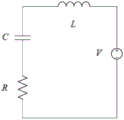
Therefore, the embodiment of the invention provides a second-order model of a field effect transistor switch loop, which is used for solving the technical problem that an electronic device is damaged due to overvoltage and electromagnetic interference possibly caused by oscillation in the transient state process of the existing silicon carbide MOSFET switch. Fig. 2 is a circuit block diagram of a second-order model of a fet switch loop according to an embodiment of the present invention, as shown in fig. 2.
The second-order model of the field effect transistor switch loop provided by the embodiment of the invention comprises a step power supply V, a main loop inductor L connected with the positive electrode of the step power supply V, a main loop capacitor C connected with the main loop inductor L and a main loop resistor R connected with the main loop capacitor C, wherein the main loop resistor R is connected with the negative electrode of the step power supply V.
The field effect transistor MOSFET may be a silicon carbide MOSFET, or may be a MOS transistor made of another material. In other embodiments, the field effect transistor MOSFET may also be a triode.
The second-order model of the field effect transistor switch loop provided by the embodiment of the invention does not need to access additional damping equipment to a main loop in the field effect transistor switch loop, and does not introduce a new oscillation mode; compared with the problem that the driving resistance of the field effect transistor is selected according to experience to inhibit the switch oscillation, the second-order model of the field effect transistor switch loop obtains the driving resistance capable of inhibiting the oscillation in the switching-on or switching-off process of the field effect transistor through switching on and switching off the second-order model, and the oscillation in the switching-on or switching-off process of the field effect transistor is effectively inhibited; the technical problem that an electronic device is damaged due to overvoltage and electromagnetic interference caused by oscillation in the transient state process of the existing silicon carbide MOSFET switch is solved.
As shown in fig. 3, fig. 3 is a circuit diagram of a second-order model of a fet switch loop according to an embodiment of the present invention during a turn-on process.
In one embodiment of the invention, the second-order model of the field effect transistor switch loop is in a turn-on process, the diode D is in a reverse bias state, and the first capacitor CJIn a charging state, drain-source capacitance CDSShorted, gate-drain capacitance CGDAnd gate source capacitance CGSThe parallel connection, the voltage between the drain electrode of the field effect transistor MOSFET and the source electrode thereof is kept unchanged; the second order model of the FET switching circuit includes a first stage power supply V (t), a main circuit inductor L 'connected to the positive electrode of the first stage power supply V (t)'loopAnd main circuit inductance L'loopConnected first capacitor CJAnd a first capacitor CJConnected first main loop resistor Req1First main loop resistance Req1Is connected to the negative electrode of the first step power supply V (t).
The second-order model of the field effect transistor switch loop is in the process of opening, the field effect transistor MOSFET can be regarded as an ideal device, the field effect transistor MOSFET is in a conducting state, the diode D is in reverse bias, and the first capacitor CJIn a charging state, the source and drain of the field effect transistor MOSFET are on, and the resistor R of the field effect transistor MOSFET with the source and drain thereof onDS(ON)Directly connected with the first capacitor CJConnected, drain-source capacitance CDSShorted, gate-drain capacitance CGDAnd gate source capacitance CGSAre connected in parallel. Voltage V between drain and source of field effect transistor MOSFET during transient state due to MOSFET turn-onDSThe electronic component of the field effect transistor MOSFET can be regarded as a damping resistor, so that a circuit of a switching process of a field effect transistor switching loop is simplified, and a second-order model of the switching process of the field effect transistor switching loop is obtained, wherein the second-order model of the field effect transistor switching loop comprises a first-order power supply V (t) and a main loop inductor L 'connected with a positive electrode of the first-order power supply V (t)'loopAnd main circuit inductance L'loopConnected first capacitor CJAnd a first capacitor CJConnected first main loop resistor Req1First main loop resistance Req1Is connected to the negative electrode of the first step power supply V (t).
The first capacitor CJThe voltage of the first step power supply V (t) is stepped from 0V to the first power supply V for the junction capacitance of the diode DDCThe voltage of (c). Specifically, the main circuit inductance L'loopThe formula of (1) is:
L'loop=Lloop+LD
first main loop resistor Req1The formula of (1) is:
wherein, ω isONThe second-order model of the field effect transistor switch loop is the resonant frequency in the switching-on process.
The characteristic equation of the second-order model of the field effect transistor switch loop is as follows:
and s is a complex frequency domain variable after Laplace transform (Laplace) transform. Wherein, the characteristic equation of the second-order system is as follows:
wherein is the damping coefficient (damping ratio) of xi system, omeganIs the natural oscillation angular frequency of the system. According to the second-order model characteristic equation derived in the invention, the natural oscillation angular frequency is obtained as follows:
obtaining a damping coefficient xi of a second-order model of the field effect transistor switch loop in the process of opening according to the characteristic equation1,ξ1The formula of (1) is:
according to the obtained damping coefficient xi1The time t required by the second-order model of the field effect transistor switch loop in the switching-on process can be obtainedr1,tr1The formula of (1) is:
as shown in fig. 4, fig. 4 is a circuit diagram of a second-order model shutdown process of a field effect transistor switch loop according to an embodiment of the present invention.
In one embodiment of the invention, the second-order model of the FET switch loop is in the turn-off process, and the drain-source capacitance C in the FET switch loopDSIn a charging state, the first capacitor CJShort-circuited, the drain of the field effect transistor MOSFET and the source thereof are in an off-state; the second-order model of the FET switching circuit includes a second step-up power supply V (t) ', and a main circuit inductor L ' connected to the positive pole of the second step-up power supply V (t) '.loopAnd main circuit inductance L'loopConnected equivalent capacitance CDAnd equivalent capacitance CDConnected second main loop resistor Req2Second main loop resistor Req2Is connected with the negative pole of the second step-up power supply V (t)'.
The second-order model of the field effect transistor switch loop is in the turn-off process, the MOSFET is in the cut-off state, and the drain-source capacitor CDSIn a charging state, the first capacitor CJThe second-order model of the field effect transistor switch circuit, which is obtained by simplifying a circuit in a turn-off process of a second-order model of the field effect transistor switch circuit including a second step-up power source V (t) 'and a main circuit inductance L' connected to a positive electrode of the second step-up power source V (t) 'and is short-circuited, with the source and the drain of the field effect transistor MOSFET being turned off and the source and the drain of the field effect transistor MOSFET being disconnected from each other, is provided'loopAnd main circuit inductance L'loopConnected equivalent capacitance CDAnd equivalent capacitance CDConnected second main loop resistor Req2Second main loop resistor Req2Is connected with the negative pole of the second step-up power supply V (t)'. Wherein switching off comprises switching off and or switching off.
It should be noted that the equivalent capacitance CDIs a gate-drain capacitor CGDGate source capacitance CGSAnd a drain-source capacitance CDSThe voltage of the second step-up power supply V (t)' is converted from the first power supply VDCStepped to 0V. Specifically, the main circuit inductance L'loopThe formula of (1) is:
L'loop=Lloop+LD
second main loop resistor Req2The formula of (1) is:
wherein, ω isONFor the resonant frequency, C, of the second-order model of the field effect transistor switching circuit during the turn-off processSIs the source side equivalent capacitance, C, of a MOSFETGIs the gate side equivalent capacitance of a field effect transistor MOSFET.
The second-order model of the field effect transistor switch loop is in the turn-off process, and the characteristic equation of the second-order model of the field effect transistor switch loop is as follows:
and s is a complex frequency domain variable after Laplace transform (Laplace) transform.
Obtaining a damping coefficient xi of the second-order model of the field effect transistor switch loop in the turn-off process according to the characteristic equation of the second-order system and the characteristic equation of the second-order model of the field effect transistor switch loop2,ξ2The formula of (1) is:
according to the obtained damping coefficient xi2The time t required by the second-order model of the field effect transistor switch loop in the turn-off process can be obtainedr2,tr2The formula of (1) is:
the smaller the damping coefficient of the field effect transistor is, the more serious the oscillation generated in the on or off process of the field effect transistor is, the damping coefficient of the field effect transistor is less than 1 in the on or off process under normal operation, and the field effect transistor is in an underdamped state. In a second-order model of the field effect transistor switch loop, the driving resistor R can be adjustedGChanging the equivalent first main loop resistance Req1Or a second main loop resistor Req2The damping coefficient is increased, and the oscillation of the field effect transistor MOSEFT in the on-off process is restrained.
In the second-order model of the fet switch circuit, in order to suppress switching oscillation while ensuring fast response of the fet mosfet, the damping coefficient ξ is1And xi2Preferably 0.8, i.e. ξ1=ξ2=0.8。
Example two:
in addition, the switching speed is required when the field effect transistor is appliedHigher, time requirement for the field effect transistor to be on or off, and thus according to the damping coefficient ξ1Or/and xi2Adjusting the drive resistance RG. Referring to fig. 5, fig. 5 is a flowchart illustrating steps of a control method for suppressing switching oscillation of a field effect transistor according to an embodiment of the present invention. The invention provides a control method for inhibiting field effect transistor switch oscillation, which comprises the following steps:
s1, acquiring a second-order model of a field effect transistor switch loop;
s2, obtaining a damping coefficient with the least time required in the switching-on and switching-off processes in a second-order model of the field effect transistor switch loop according to the second-order model;
s3, comparing the obtained damping coefficient with a preset value of the damping coefficient, taking the minimum value to obtain a new damping coefficient xi in the switching-on process of the field effect transistor switch loopopt1And damping coefficient xi of the turn-off processopt2;
S4, according to the obtained damping coefficient xiopt1And xiopt2And calculating the driving resistance for inhibiting oscillation of the field effect transistor in the switching-on or switching-off process in the second-order model.
In the embodiment of the present invention, when the damping coefficient of the field effect transistor MOSFET is less than 1, the larger the damping coefficient is, the longer the time required for the field effect transistor MOSFET to be turned on (on) or turned off (off) is, and the slower the switching speed for turning on or off the field effect transistor MOSFET is. Therefore, in order to achieve reasonable suppression of switching oscillation of the field effect transistor MOSFET during on or off, it is necessary to conduct research between the damping coefficient of the field effect transistor MOSFET and the time required for on or off of the field effect transistor MOSFET. If the time required for turning on or off the MOSFET is minimal, the time is denoted as tminWill tminIs sleeved in tr1Formula (ii) and tr2In the formula (2), the damping coefficient xi 'of which the time required for the on or off process of the field effect transistor MOSFET is minimum is obtained'1And ξ'2And obtaining a damping coefficient of ξ'1And ξ'2Comparing with a preset value of 0.8, selecting xi'1Minimum value compared to 0.8 and is noted as ξopt1(ii) a Selecting xi2Minimum value of' compared to 0.8 and is noted as ξopt2. The obtained damping coefficient xiopt1Is sleeved in xi1And a first main loop resistance Req1Obtaining a driving resistance optimization design value R for inhibiting the switch oscillation in the process of the MOSFET conduction of the field effect transistorG(ON)-opt(ii) a The obtained damping coefficient xiopt2Is sleeved in xi2And a second main loop resistance Req2Obtaining a driving resistance optimization design value R for inhibiting the switch oscillation in the cut-off process of the MOSFET of the field effect transistorG(OFF)-opt。
In an embodiment of the invention ξopt1Optimizing damping coefficient, ξ, for damping switching oscillations during the conduction of a field effect transistor MOSFETopt2The damping coefficient is optimized for inhibiting the switch oscillation in the cut-off process of the MOSFET.
The off state of the field effect transistor MOSFET may be an off state of the field effect transistor MOSFET or an off state.
In one embodiment of the invention, the preset value of the damping coefficient is 0.6-0.8. Preferably, the preset value of the damping coefficient is 0.8.
The control method for inhibiting the switching oscillation of the field effect transistor obtains the damping coefficient with the least time required by the switching-on and switching-off processes of the field effect transistor through a second-order model of a switching loop of the field effect transistor, then compares the damping coefficient with the preset damping coefficient value to obtain a new damping coefficient, and obtains the driving resistance for inhibiting the oscillation of the field effect transistor in the switching-on or switching-off process according to the new damping coefficient in the second-order model. Compared with the existing method for selecting the driving resistor by depending on experience to inhibit the switching oscillation of the field effect transistor, the control method for inhibiting the switching oscillation of the field effect transistor is more reasonable and has high efficiency; switch oscillation of the field effect transistor in the switching-on and switching-off processes is effectively inhibited according to the selected driving resistor, and the technical problem that an electronic device is damaged due to overvoltage and electromagnetic interference possibly caused by oscillation in the transient state process of the existing silicon carbide MOSFET switch is solved.
It is clear to those skilled in the art that, for convenience and brevity of description, the specific working processes of the above-described systems, apparatuses and units may refer to the corresponding processes in the foregoing method embodiments, and are not described herein again.
In the several embodiments provided in the present application, it should be understood that the disclosed system, apparatus and method may be implemented in other manners. For example, the above-described apparatus embodiments are merely illustrative, and for example, the division of the units is only one logical division, and other divisions may be realized in practice, for example, a plurality of units or components may be combined or integrated into another system, or some features may be omitted, or not executed. In addition, the shown or discussed mutual coupling or direct coupling or communication connection may be an indirect coupling or communication connection through some interfaces, devices or units, and may be in an electrical, mechanical or other form.
The units described as separate parts may or may not be physically separate, and parts displayed as units may or may not be physical units, may be located in one place, or may be distributed on a plurality of network units. Some or all of the units can be selected according to actual needs to achieve the purpose of the solution of the embodiment.
In addition, functional units in the embodiments of the present invention may be integrated into one processing unit, or each unit may exist alone physically, or two or more units are integrated into one unit. The integrated unit can be realized in a form of hardware, and can also be realized in a form of a software functional unit.
The integrated unit, if implemented in the form of a software functional unit and sold or used as a stand-alone product, may be stored in a computer readable storage medium. Based on such understanding, the technical solution of the present invention may be embodied in the form of a software product, which is stored in a storage medium and includes instructions for causing a computer device (which may be a personal computer, a server, or a network device) to execute all or part of the steps of the method according to the embodiments of the present invention. And the aforementioned storage medium includes: a U-disk, a removable hard disk, a Read-Only Memory (ROM), a Random Access Memory (RAM), a magnetic disk or an optical disk, and other various media capable of storing program codes.
The above-mentioned embodiments are only used for illustrating the technical solutions of the present invention, and not for limiting the same; although the present invention has been described in detail with reference to the foregoing embodiments, it will be understood by those of ordinary skill in the art that: the technical solutions described in the foregoing embodiments may still be modified, or some technical features may be equivalently replaced; and such modifications or substitutions do not depart from the spirit and scope of the corresponding technical solutions of the embodiments of the present invention.