CN110649047A - Photosensitive chip package structure and method of forming the same - Google Patents
Photosensitive chip package structure and method of forming the same Download PDFInfo
- Publication number
- CN110649047A CN110649047A CN201810669963.9A CN201810669963A CN110649047A CN 110649047 A CN110649047 A CN 110649047A CN 201810669963 A CN201810669963 A CN 201810669963A CN 110649047 A CN110649047 A CN 110649047A
- Authority
- CN
- China
- Prior art keywords
- photosensitive chip
- protective glass
- photosensitive
- area
- circuit board
- Prior art date
- Legal status (The legal status is an assumption and is not a legal conclusion. Google has not performed a legal analysis and makes no representation as to the accuracy of the status listed.)
- Pending
Links
Images





Classifications
-
- H—ELECTRICITY
- H10—SEMICONDUCTOR DEVICES; ELECTRIC SOLID-STATE DEVICES NOT OTHERWISE PROVIDED FOR
- H10F—INORGANIC SEMICONDUCTOR DEVICES SENSITIVE TO INFRARED RADIATION, LIGHT, ELECTROMAGNETIC RADIATION OF SHORTER WAVELENGTH OR CORPUSCULAR RADIATION
- H10F39/00—Integrated devices, or assemblies of multiple devices, comprising at least one element covered by group H10F30/00, e.g. radiation detectors comprising photodiode arrays
- H10F39/80—Constructional details of image sensors
- H10F39/804—Containers or encapsulations
-
- H—ELECTRICITY
- H10—SEMICONDUCTOR DEVICES; ELECTRIC SOLID-STATE DEVICES NOT OTHERWISE PROVIDED FOR
- H10F—INORGANIC SEMICONDUCTOR DEVICES SENSITIVE TO INFRARED RADIATION, LIGHT, ELECTROMAGNETIC RADIATION OF SHORTER WAVELENGTH OR CORPUSCULAR RADIATION
- H10F39/00—Integrated devices, or assemblies of multiple devices, comprising at least one element covered by group H10F30/00, e.g. radiation detectors comprising photodiode arrays
- H10F39/011—Manufacture or treatment of image sensors covered by group H10F39/12
- H10F39/018—Manufacture or treatment of image sensors covered by group H10F39/12 of hybrid image sensors
-
- H—ELECTRICITY
- H10—SEMICONDUCTOR DEVICES; ELECTRIC SOLID-STATE DEVICES NOT OTHERWISE PROVIDED FOR
- H10F—INORGANIC SEMICONDUCTOR DEVICES SENSITIVE TO INFRARED RADIATION, LIGHT, ELECTROMAGNETIC RADIATION OF SHORTER WAVELENGTH OR CORPUSCULAR RADIATION
- H10F39/00—Integrated devices, or assemblies of multiple devices, comprising at least one element covered by group H10F30/00, e.g. radiation detectors comprising photodiode arrays
- H10F39/80—Constructional details of image sensors
- H10F39/809—Constructional details of image sensors of hybrid image sensors
-
- H—ELECTRICITY
- H10—SEMICONDUCTOR DEVICES; ELECTRIC SOLID-STATE DEVICES NOT OTHERWISE PROVIDED FOR
- H10F—INORGANIC SEMICONDUCTOR DEVICES SENSITIVE TO INFRARED RADIATION, LIGHT, ELECTROMAGNETIC RADIATION OF SHORTER WAVELENGTH OR CORPUSCULAR RADIATION
- H10F71/00—Manufacture or treatment of devices covered by this subclass
-
- H—ELECTRICITY
- H10—SEMICONDUCTOR DEVICES; ELECTRIC SOLID-STATE DEVICES NOT OTHERWISE PROVIDED FOR
- H10F—INORGANIC SEMICONDUCTOR DEVICES SENSITIVE TO INFRARED RADIATION, LIGHT, ELECTROMAGNETIC RADIATION OF SHORTER WAVELENGTH OR CORPUSCULAR RADIATION
- H10F77/00—Constructional details of devices covered by this subclass
- H10F77/30—Coatings
- H10F77/306—Coatings for devices having potential barriers
- H10F77/331—Coatings for devices having potential barriers for filtering or shielding light, e.g. multicolour filters for photodetectors
- H10F77/334—Coatings for devices having potential barriers for filtering or shielding light, e.g. multicolour filters for photodetectors for shielding light, e.g. light blocking layers or cold shields for infrared detectors
-
- H—ELECTRICITY
- H10—SEMICONDUCTOR DEVICES; ELECTRIC SOLID-STATE DEVICES NOT OTHERWISE PROVIDED FOR
- H10F—INORGANIC SEMICONDUCTOR DEVICES SENSITIVE TO INFRARED RADIATION, LIGHT, ELECTROMAGNETIC RADIATION OF SHORTER WAVELENGTH OR CORPUSCULAR RADIATION
- H10F77/00—Constructional details of devices covered by this subclass
- H10F77/30—Coatings
- H10F77/306—Coatings for devices having potential barriers
- H10F77/331—Coatings for devices having potential barriers for filtering or shielding light, e.g. multicolour filters for photodetectors
- H10F77/337—Coatings for devices having potential barriers for filtering or shielding light, e.g. multicolour filters for photodetectors using interference filters, e.g. multilayer dielectric filters
-
- H—ELECTRICITY
- H10—SEMICONDUCTOR DEVICES; ELECTRIC SOLID-STATE DEVICES NOT OTHERWISE PROVIDED FOR
- H10F—INORGANIC SEMICONDUCTOR DEVICES SENSITIVE TO INFRARED RADIATION, LIGHT, ELECTROMAGNETIC RADIATION OF SHORTER WAVELENGTH OR CORPUSCULAR RADIATION
- H10F77/00—Constructional details of devices covered by this subclass
- H10F77/40—Optical elements or arrangements
- H10F77/413—Optical elements or arrangements directly associated or integrated with the devices, e.g. back reflectors
-
- H—ELECTRICITY
- H10—SEMICONDUCTOR DEVICES; ELECTRIC SOLID-STATE DEVICES NOT OTHERWISE PROVIDED FOR
- H10F—INORGANIC SEMICONDUCTOR DEVICES SENSITIVE TO INFRARED RADIATION, LIGHT, ELECTROMAGNETIC RADIATION OF SHORTER WAVELENGTH OR CORPUSCULAR RADIATION
- H10F77/00—Constructional details of devices covered by this subclass
- H10F77/50—Encapsulations or containers
-
- H—ELECTRICITY
- H10—SEMICONDUCTOR DEVICES; ELECTRIC SOLID-STATE DEVICES NOT OTHERWISE PROVIDED FOR
- H10F—INORGANIC SEMICONDUCTOR DEVICES SENSITIVE TO INFRARED RADIATION, LIGHT, ELECTROMAGNETIC RADIATION OF SHORTER WAVELENGTH OR CORPUSCULAR RADIATION
- H10F77/00—Constructional details of devices covered by this subclass
- H10F77/93—Interconnections
- H10F77/933—Interconnections for devices having potential barriers
Landscapes
- Solid State Image Pick-Up Elements (AREA)
- Engineering & Computer Science (AREA)
- Transforming Light Signals Into Electric Signals (AREA)
- Microelectronics & Electronic Packaging (AREA)
- Manufacturing & Machinery (AREA)
Abstract
一种感光芯片封装结构,其包括:电路板;设置于电路板上、与电路板电性导通的感光芯片,所述感光芯片包括感光区以及环绕所述感光区的非感光区;保护玻璃,所述保护玻璃的尺寸大于所述感光区的尺寸,所述保护玻璃完全覆盖所述感光区,所述保护玻璃在光路方向上定义有透光区与环绕所述透光区的边缘区;以及封装结构,所述封装结构不透光,所述封装结构包覆所述感光芯片及保护玻璃的侧壁且覆盖所述保护玻璃的所述边缘区以在所述保护玻璃的边缘区形成挡光层,所述封装结构、所述保护玻璃、所述感光芯片及所述电路板形成为一体。

A photosensitive chip package structure, comprising: a circuit board; a photosensitive chip disposed on the circuit board and electrically connected to the circuit board, the photosensitive chip comprising a photosensitive area and a non-photosensitive area surrounding the photosensitive area; a protective glass , the size of the protective glass is larger than the size of the photosensitive area, the protective glass completely covers the photosensitive area, and the protective glass defines a light-transmitting area and an edge area surrounding the light-transmitting area in the direction of the optical path; and an encapsulation structure, the encapsulation structure is opaque to light, the encapsulation structure covers the photosensitive chip and the sidewall of the protective glass and covers the edge area of the protective glass to form a barrier on the edge area of the protective glass The optical layer, the encapsulation structure, the protective glass, the photosensitive chip and the circuit board are formed into one body.
Description
技术领域technical field
本发明涉及一种用于相机模组中的感光芯片封装结构及其形成方法。The invention relates to a photosensitive chip packaging structure used in a camera module and a method for forming the same.
背景技术Background technique
现有技术中,感光芯片都是通过模塑于芯片的方式(Molding on chip,MOC)形成于电路板上,具体地,在模塑之前,是先将感光芯片设置于电路板,再对电路板及感光芯片实现电性导通,再在感光芯片周围侧射出成型使封装体将感光芯片及电路板形成于一体得到封装结构,所述封装体能为摄像模组提供支撑。将所述感光芯片封装结构用于形成摄像模组时,将镜头结构设置在所述封装体上。但是,在将封装结构与光学镜头一起形成摄像模组之前,感光芯片长时间暴露于空气中,造成落尘掉落于感光芯片上,而导致摄像模组用于摄像时会产生影像坏点。In the prior art, the photosensitive chip is formed on the circuit board by molding on chip (MOC). Specifically, before molding, the photosensitive chip is first placed on the circuit board, and then the circuit The board and the photosensitive chip are electrically connected, and then injection molding is performed around the photosensitive chip, so that the package body integrates the photosensitive chip and the circuit board to obtain a package structure, and the package body can provide support for the camera module. When the photosensitive chip package structure is used to form a camera module, the lens structure is arranged on the package body. However, before the package structure and the optical lens are formed into a camera module, the photosensitive chip is exposed to the air for a long time, which causes dust to fall on the photosensitive chip, resulting in image dead pixels when the camera module is used for imaging.
因此,有必要提供一种能克服以上技术问题的用于相机模组的感光芯片封装结构及其形成方法。Therefore, it is necessary to provide a photosensitive chip packaging structure for a camera module and a method for forming the same, which can overcome the above technical problems.
发明内容SUMMARY OF THE INVENTION
本发明目的在于提供一种能解决上述问题的感光芯片封装结构及其形成方法。The purpose of the present invention is to provide a photosensitive chip package structure and a method for forming the same which can solve the above problems.
一种感光芯片封装结构,其包括:A photosensitive chip packaging structure, comprising:
电路板;circuit board;
设置于电路板上、与电路板电性导通的感光芯片,所述感光芯片包括感光区以及环绕所述感光区的非感光区;a photosensitive chip arranged on the circuit board and electrically connected to the circuit board, the photosensitive chip includes a photosensitive area and a non-photosensitive area surrounding the photosensitive area;
保护玻璃,所述保护玻璃的尺寸大于所述感光区的尺寸,所述保护玻璃完全覆盖所述感光区,所述保护玻璃在光路方向上定义有透光区与环绕所述透光区的边缘区;以及Protective glass, the size of the protective glass is larger than the size of the photosensitive area, the protective glass completely covers the photosensitive area, and the protective glass defines a light-transmitting area and an edge surrounding the light-transmitting area in the direction of the light path district; and
封装结构,所述封装结构不透光,所述封装结构包覆所述感光芯片及保护玻璃的侧壁且覆盖所述保护玻璃的所述边缘区以在所述保护玻璃的边缘区形成挡光层,所述封装结构、所述保护玻璃、所述感光芯片及所述电路板形成为一体。an encapsulation structure, the encapsulation structure is opaque to light, the encapsulation structure covers the photosensitive chip and the sidewalls of the protective glass, and covers the edge area of the protective glass to form a light block in the edge area of the protective glass layer, the encapsulation structure, the protective glass, the photosensitive chip and the circuit board are integrated.
在一个优选实施方式中,所述封装结构包括用于支撑光学镜头的支撑面以及与支撑面垂直的侧表面,所述封装结构还包括嵌入成型有金属片,所述金属片位于所述支撑面以及侧表面。In a preferred embodiment, the package structure includes a support surface for supporting the optical lens and a side surface perpendicular to the support surface, the package structure further includes a metal sheet that is insert-molded, and the metal sheet is located on the support surface and side surfaces.
在一个优选实施方式中,所述感光区周围设置有一圈黑胶层,所述滤光片通过所述黑胶层贴设于所述感光区。In a preferred embodiment, a black rubber layer is arranged around the photosensitive area, and the optical filter is attached to the photosensitive area through the black rubber layer.
在一个优选实施方式中,所述挡光层的厚度为0.1毫米至0.3毫米。In a preferred embodiment, the thickness of the light blocking layer is 0.1 mm to 0.3 mm.
一种感光芯片封装结构的形成方法,其包括如下步骤:A method for forming a photosensitive chip package structure, comprising the following steps:
提供电路板;provide circuit boards;
提供感光芯片,并将所述感光芯片贴设于所述电路板上,所述感光芯片包括感光区及非感光区;providing a photosensitive chip, and attaching the photosensitive chip on the circuit board, the photosensitive chip includes a photosensitive area and a non-photosensitive area;
提供保护玻璃,所述保护玻璃的尺寸大于所述感光区的尺寸,将所述保护玻璃贴设于所述感光芯片的表面,所述保护玻璃完全覆盖所述感光区,所述保护玻璃在光路方向上定义有透光区与环绕所述透光区的边缘区;Provide a protective glass, the size of the protective glass is larger than the size of the photosensitive area, the protective glass is attached to the surface of the photosensitive chip, the protective glass completely covers the photosensitive area, and the protective glass is in the optical path. A light-transmitting area and an edge area surrounding the light-transmitting area are defined in the direction;
导通连接所述电路板及所述感光芯片;Conductively connect the circuit board and the photosensitive chip;
在所述电路板上模塑形成封装结构,所述封装结构不能透光,所述封装结构包覆所述感光芯片及保护玻璃的侧壁且覆盖所述保护玻璃的所述边缘区形成挡光层,所述封装结构、所述保护玻璃、所述感光芯片及所述电路板形成为一体。An encapsulation structure is formed by molding on the circuit board, the encapsulation structure cannot transmit light, the encapsulation structure covers the photosensitive chip and the sidewalls of the protective glass, and covers the edge area of the protective glass to form light blocking layer, the encapsulation structure, the protective glass, the photosensitive chip and the circuit board are integrated.
在一个优选实施方式中,所述挡光层的厚度为0.1毫米至0.3毫米。In a preferred embodiment, the thickness of the light blocking layer is 0.1 mm to 0.3 mm.
在一个优选实施方式中,提供的电路板上还设置有电子元件,所述电子元件位于所述感光芯片的周围,经过模塑形成的所述封装结构还包覆所述电子元件。In a preferred embodiment, the provided circuit board is further provided with electronic components, the electronic components are located around the photosensitive chip, and the package structure formed by molding also covers the electronic components.
在一个优选实施方式中,在模塑形成所述封装结构之前还包括在所述保护玻璃靠近所述透光区的所述设置可撕除挡墙胶,以及在形成所述封装结构之后剥离所述可撕除挡墙胶。In a preferred embodiment, before the encapsulation structure is formed by molding, it further comprises that the disposing of the protective glass near the light-transmitting area can remove the retaining wall adhesive, and after the encapsulation structure is formed, peeling off the Removable retaining wall adhesive described above.
在一个优选实施方式中,所述封装结构包括用于支撑光学镜头的支撑面以及与支撑面垂直的侧表面,形成的所述封装结构还包括嵌入成型有金属片,所述金属片位于所述支撑面以及侧表面。In a preferred embodiment, the package structure includes a support surface for supporting the optical lens and a side surface perpendicular to the support surface, and the package structure formed further includes insert molding a metal sheet, and the metal sheet is located on the Support surface and side surface.
在一个优选实施方式中,所述感光区周围设置有一圈黑胶层,所述滤光片是通过所述黑胶层贴设于所述感光区。In a preferred embodiment, a circle of black glue layer is arranged around the photosensitive area, and the optical filter is attached to the photosensitive area through the black glue layer.
与现有技术相比较,本发明提供的感光芯片封装结构的形成方法及由此形成的感光芯片封装结构,由于是在形成感光芯片之后直接在感光芯片表面设置保护玻璃,减少了感光芯片暴露在空气中的时间,从而避免了落尘掉落于感光芯片上,进而避免了摄像模组用于摄像时产生影像坏点对比现象产生。Compared with the prior art, in the method for forming a photosensitive chip package structure and the photosensitive chip package structure formed therefrom, the protective glass is directly placed on the surface of the photosensitive chip after the photosensitive chip is formed, which reduces the exposure of the photosensitive chip to the surface of the photosensitive chip. The time in the air can prevent the dust from falling on the photosensitive chip, thereby avoiding the contrast phenomenon of image dead pixels when the camera module is used for shooting.
附图说明Description of drawings
图1为本发明第一实施例提供的电路板的剖面图。FIG. 1 is a cross-sectional view of a circuit board according to a first embodiment of the present invention.
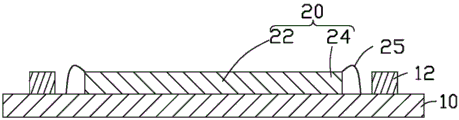
图2为在图1所示的电路板上设置感光芯片的剖面图。FIG. 2 is a cross-sectional view of disposing a photosensitive chip on the circuit board shown in FIG. 1 .
图3为电性导通电路板及感光芯片的剖面图。FIG. 3 is a cross-sectional view of an electrically conductive circuit board and a photosensitive chip.
图4为在感光芯片的表面设置保护玻璃的剖面图。FIG. 4 is a cross-sectional view of providing a protective glass on the surface of the photosensitive chip.
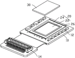
图5为提供的保护玻璃的立体结构图。FIG. 5 is a perspective structural view of the provided protective glass.
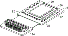
图6为在感光芯片表面设置保护玻璃的立体结构图。FIG. 6 is a three-dimensional structural view of disposing protective glass on the surface of the photosensitive chip.
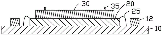
图7为在所述保护玻璃的表面设置可撕除挡墙胶的剖面图。FIG. 7 is a cross-sectional view of disposing a removable retaining wall glue on the surface of the protective glass.
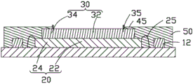
图8为模塑形成封装结构后得到感光芯片封装结构的剖面图。FIG. 8 is a cross-sectional view of a photosensitive chip package structure obtained after molding the package structure.
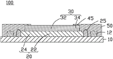
图9为移除可撕除挡墙胶得到感光芯片封装结构的剖面图。FIG. 9 is a cross-sectional view of a photosensitive chip package structure obtained by removing the peelable retaining wall adhesive.
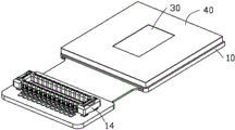
图10为感光芯片封装结构的立体结构图。FIG. 10 is a perspective structural view of a photosensitive chip packaging structure.
图11是将感光芯片封装结构形成摄像模组的剖面图。FIG. 11 is a cross-sectional view of forming a photosensitive chip package structure into a camera module.
图12是本本发明第二实施例提供的芯片封装结构的剖面图。12 is a cross-sectional view of a chip package structure provided by a second embodiment of the present invention.
主要元件符号说明Description of main component symbols
感光芯片封装结构 100,200Photosensitive
电路板 10
摄像模组 110
感光芯片 20
封装结构 40,401
电路元件 12
电连接器 14
感光区 22
非感光区 24Non-photosensitive
黑胶层 26
保护玻璃 30
导线 25
可撕除挡墙胶 35Removable
边缘区 34
挡光层 45
透光区 32
支撑面 42,420
侧表面 44
金属片 50
光学镜头 60
镜片 62
如下具体实施方式将结合上述附图进一步说明本发明。The following specific embodiments will further illustrate the present invention in conjunction with the above drawings.
具体实施方式Detailed ways
下面将结合附图,对本发明提供的承载座及其形成方法及相机模组进一步的详细的说明。The bearing seat and its forming method and the camera module provided by the present invention will be further described in detail below with reference to the accompanying drawings.
需要说明的是,当元件被称为“固定于”、“设置于”或“安装于”另一个元件,它可以直接在另一个元件上或者间接在该另一个元件上。当一个元件被称为是“连接于”另一个元件,它可以是直接连接到另一个元件或间接连接至该另一个元件上。另外,连接即可以是用于固定作用也可以是用于电路连通作用。It should be noted that when an element is referred to as being "fixed on", "disposed on" or "mounted on" another element, it can be directly on the other element or indirectly on the other element. When an element is referred to as being "connected to" another element, it can be directly connected to the other element or indirectly connected to the other element. In addition, the connection can be used for either a fixing function or a circuit connecting function.
需要理解的是,术语“长度”、“宽度”、“上”、“下”、“前”、“后”、“左”、“右”、“竖直”、“水平”、“顶”、“底”“内”、“外”等指示的方位或位置关系为基于附图所示的方位或位置关系,仅是为了便于描述本发明实施例和简化描述,而不是指示或暗示所指的装置或元件必须具有特定的方位、以特定的方位构造和操作,因此不能理解为对本发明的限制。It is to be understood that the terms "length", "width", "upper", "lower", "front", "rear", "left", "right", "vertical", "horizontal", "top" , "bottom", "inside", "outside", etc. indicate the orientation or positional relationship based on the orientation or positional relationship shown in the accompanying drawings, which are only for the convenience of describing the embodiments of the present invention and simplifying the description, rather than indicating or implying that The device or element must have a specific orientation, be constructed and operated in a specific orientation, and therefore should not be construed as a limitation of the present invention.
请参阅图1至图10,为本发明提供的一种感光芯片封装结构的形成方法。其包括如下步骤:Please refer to FIG. 1 to FIG. 10 , which illustrate a method for forming a photosensitive chip package structure provided by the present invention. It includes the following steps:
第一步:请参阅图1,提供电路板10;所述电路板10上设置有电路元件12及电连接器14。所述电路板10可以选择为但不限于,软硬结合板、陶瓷基板、PCB硬板等。在本实施方式中,所述电路元件12设置于电路板的边缘位置,电路板10的中央位置用于设置感光芯片20。所述电路元件12电连接于所述感光芯片20,以供所述感光芯片20的感光工作过程。所述电路元件12可以是,但不限于,电阻、电容、二极管、三极管、电位器、继电器或驱动器等。所述电连接器14与所述感光芯片20电性连接,以实现感光芯片20与电子装置的信号传输。The first step: referring to FIG. 1 , a
第二步:请参阅图2及图3,提供感光芯片20,并将所述感光芯片20贴设于所述电路板10上且导通所述感光芯片20及所述电路板10。例如,利用导线25电连接以导通所述感光芯片20和所述电路板10。在本实施方式中,电路板10上、感光芯片20上分别预设有导电垫,导线25的两端分别连接电路板10及感光芯片20上的导电垫。所述导线25可以被实施为不必限于,金线、铜线、铝线、银线等。特别地,所述导线25呈弧形地连接所述感光芯片20所述电路板10,从而避免所述导线25出现弯折损伤。Step 2: Please refer to FIG. 2 and FIG. 3 , provide a
所述感光芯片20包括感光区22及环绕所述感光区22的非感光区24。所述感光区22用于进行感光作用。譬如,可以是在所述非感光区24设置一圈黑胶层26,所述黑胶层26环绕所述感光区22,以利用所述黑胶层26固定后续的保护玻璃30。在本案的剖面图图4中,由于黑胶层26非常薄,所以剖面图并未示意,在图5可以看到黑胶层26。The
第三步:请参阅图4及图5及图6,提供保护玻璃30并将其设置于所述感光芯片20的表面,在本实施方式中,所述保护玻璃30是滤光片,从而自所述光学镜头进入所述摄像模组110的内部的光线首先通过所述滤光片的过滤,然后被所述感光芯片20接收以在后续进行光电转化。例如在本发明的一个优选的实施例中,所述保护玻璃30可以被实施为红外截止滤光片,其能够过滤自所述光学镜头进入所述摄像模组110的内部的光线中的红外线部分,从而有利于提高所述摄像模组110的成像品质。当然,所述保护玻璃30也可以是透明的片状体。所述保护玻璃30的尺寸大于所述感光区22的尺寸,将所述保护玻璃30贴设于所述感光区22,以利用保护玻璃30覆盖所述感光芯片20以对感光芯片20进行保护。所述保护玻璃30定义有透光区32与环绕所述透光区32的边缘区34。Step 3: Please refer to FIG. 4 , FIG. 5 and FIG. 6 , provide a
第四步:请参阅图7,在所述保护玻璃30的靠近所述透光区32的所述边缘区34设置可撕除挡墙胶35;可撕除挡墙胶35是对所述透光区32进行阻挡,防止在模塑形成封装结构的时模塑材料进入所述透光区32。Step 4: Referring to FIG. 7 , a
第五步:请参阅图8,在所述电路板10上模塑形成封装结构40,所述封装结构40不透光,所述封装结构40包覆所述感光芯片20及保护玻璃30的侧壁且覆盖所述保护玻璃的所述边缘区34以形成挡光层45。由于模塑材料是通过流动覆盖于所述保护玻璃30的边缘区34,从而,本发明中覆盖的厚度,也即挡光层45的厚度控制在0.1毫米至0.3毫米之间,覆盖的区域可以延伸至感光区22的正上方。所述封装结构40、所述保护玻璃30、所述感光芯片20及所述电路板10形成为一体。Step 5: Referring to FIG. 8 , an
在此,封装结构40的材质为不透明,譬如为黑色或者深色系,并且,通过使封装结构40覆盖保护玻璃30的边缘区34形成挡光层45,由于挡光层45不透光,从而能吸收从光学镜头进入摄像模组的杂散光线,防止鬼影的产生。如此,也不需要再在保护玻璃30的边缘区涂布黑漆来吸收杂散光,以减少保护玻璃的生产成本。所述封装结构40形成的方式可以选择为但不限于,注塑工艺、模压工艺等。所述封装结构40可以选择的材料为但不限于,注塑工艺可以选择尼龙、LCP(Liquid Crystal Polymer,液晶高分子聚合物)、PP(Polypropylene,聚丙烯)等,模压工艺可以采用树脂。所述封装结构40包将所述电路元件包覆于其内部,因此使得所述电路元件12不会直接暴露于空间内。Here, the material of the
第六步:请参阅图9及图10,剥离所述可撕除挡墙胶35。可撕除挡墙胶35在模塑形成所述封装结构40之后再移除,不占据保护玻璃30上的透光区32,确保设置在封装结构40上的摄像模组能吸收更多的光线。Step 6: Referring to Figure 9 and Figure 10, peel off the removable
本发明利用保护玻璃30覆盖所述感光芯片20的表面,以对所述感光芯片20进行保护,减少了感光芯片20暴露在空气中的时间,从而避免了落尘掉落于感光芯片20上,进而避免了摄像模组110用于摄像时产生影像坏点现象产生。In the present invention, the
另外,本案通过使封装结构40包覆所述保护玻璃的边缘区34形成挡光层45,利用挡光层吸收杂散光线,无需再在保护玻璃30表面网印形成黑漆,节省了保护玻璃30的制造成本。In addition, in this case, a light-blocking
请参阅图11,为将所述感光芯片封装结构100用于形成的摄像模组110,光学镜头60固设于所述封装结构40的支撑面42,光学镜头60的光路方向与所述感光区22对应。光学镜头60可以是定焦镜头、变焦镜头等。Please refer to FIG. 11 , in order to use the photosensitive
光学镜头60可以包括一至多个镜片62。本发明由于所述挡光层45的存在,如此相当于在摄像模组110的整体高度中增加了一个挡光层45的厚度,如此是拉大了镜片62与保护玻璃30的距离,减少了将光学镜头60组装至感光芯片封装结构100时,镜片62与保护玻璃30之间由于距离太近造成干涉导致保护玻璃30碎裂的风险。
请再次参阅图9及图10,为利用上述感光芯片封装结构的制作方法制作形成的感光芯片封装结构100。其包括电路板10、感光芯片20、保护玻璃30以及封装结构40。所述感光芯片20设置于电路板10上、与电路板10电性导通。所述感光芯片20包括感光区22及环绕所述感光区的非感光区24。所述感光区22用于进行感光作用。Please refer to FIG. 9 and FIG. 10 again, which are a photosensitive
所述保护玻璃30的尺寸大于所述感光区22的尺寸,所述保护玻璃30通过黑胶贴设于所述非感光区24,所述保护玻璃30定义有透光区32与环绕所述透光区32的边缘区34。The size of the
所述封装结构40不透光,所述封装结构40可以为黑色的尼龙、LCP(LiquidCrystal Polymer,液晶高分子聚合物)、或者PP(Polypropylene,聚丙烯)等。所述封装结构40包覆所述感光芯片20及保护玻璃30的侧壁且覆盖所述保护玻璃30的所述边缘区34以形成挡光层45,所述封装结构40、所述保护玻璃30、所述感光芯片20及所述电路板形成为一体。所述挡光层45不透光,从而能吸收从光学镜头进入摄像模组的杂散光线,防止鬼影的产生。挡光层45的厚度控制在0.1毫米至0.3毫米之间,覆盖的区域可以延伸至所述感光区22的正上方。由于挡光层45的厚度非常薄,从而可以避免挡光层45的侧面对光线产生反射而形成杂散光。The
请参阅图12,为本发明第二实施例提供的一种感光芯片封装结构200,所述感光芯片封装结构200的结构域第一实施例提供的感光芯片封装结构100基本相同,其不同之处在于:所述封装结构401包括用于支撑光学镜头的支撑面420以及与支撑面垂直的侧表面44,形成的所述封装结构401还包括嵌入成型有金属片50,所述金属片50位于所述支撑面420以及侧表面44。所述金属片50用于加强所述封装结构40的强度。Please refer to FIG. 12 , which is a photosensitive
所述感光芯片封装结构200大致呈方形形状,其包括四个垂直的侧表面44。所述金属片50大致呈L形状,所述金属片50形成于每个侧表面44以及与该侧表面44连接的支撑面420。也即,所述金属片50的数量为4个,且依次相互间隔。覆盖在支撑面420上的金属片50是位于所述非感光区24的上方。The photosensitive
对于本领域的技术人员来说可以在本发明技术构思内做其他变化,但是,根据本发明的技术构思做出其它各种相应的改变与变形,都应属于本发明权利要求的保护范围。For those skilled in the art, other changes can be made within the technical concept of the present invention, but various other corresponding changes and deformations made according to the technical concept of the present invention shall fall within the protection scope of the claims of the present invention.
Claims (10)
Priority Applications (3)
| Application Number | Priority Date | Filing Date | Title |
|---|---|---|---|
| CN201810669963.9A CN110649047A (en) | 2018-06-26 | 2018-06-26 | Photosensitive chip package structure and method of forming the same |
| TW107122702A TWI698009B (en) | 2018-06-26 | 2018-06-29 | Image sensor chip encapsulation structure and method for manufacturing same |
| US16/201,959 US10749046B2 (en) | 2018-06-26 | 2018-11-27 | Encapsulation structure for image sensor chip and method for manufacturing the same |
Applications Claiming Priority (1)
| Application Number | Priority Date | Filing Date | Title |
|---|---|---|---|
| CN201810669963.9A CN110649047A (en) | 2018-06-26 | 2018-06-26 | Photosensitive chip package structure and method of forming the same |
Publications (1)
| Publication Number | Publication Date |
|---|---|
| CN110649047A true CN110649047A (en) | 2020-01-03 |
Family
ID=68982182
Family Applications (1)
| Application Number | Title | Priority Date | Filing Date |
|---|---|---|---|
| CN201810669963.9A Pending CN110649047A (en) | 2018-06-26 | 2018-06-26 | Photosensitive chip package structure and method of forming the same |
Country Status (3)
| Country | Link |
|---|---|
| US (1) | US10749046B2 (en) |
| CN (1) | CN110649047A (en) |
| TW (1) | TWI698009B (en) |
Cited By (4)
| Publication number | Priority date | Publication date | Assignee | Title |
|---|---|---|---|---|
| CN112702498A (en) * | 2020-12-29 | 2021-04-23 | 维沃移动通信有限公司 | Camera module and electronic equipment |
| CN113500839A (en) * | 2021-07-16 | 2021-10-15 | 京东方科技集团股份有限公司 | Chip protection film material, electronic equipment assembling method and electronic equipment |
| CN115985972A (en) * | 2022-12-13 | 2023-04-18 | 南通敏顺智能科技有限公司 | Packaging structure of an optical sensor |
| WO2023070443A1 (en) * | 2021-10-28 | 2023-05-04 | 深圳市大疆创新科技有限公司 | Diode chip packaging structure and method, distance measuring device, and movable platform |
Families Citing this family (6)
| Publication number | Priority date | Publication date | Assignee | Title |
|---|---|---|---|---|
| CN109510925A (en) * | 2017-09-15 | 2019-03-22 | 南昌欧菲光电技术有限公司 | Camera module |
| CN111355871A (en) * | 2018-12-21 | 2020-06-30 | 三赢科技(深圳)有限公司 | Lens module and assembling method thereof |
| KR102248527B1 (en) * | 2019-05-02 | 2021-05-06 | 삼성전기주식회사 | Image sensor package |
| CN215069988U (en) * | 2021-02-01 | 2021-12-07 | 北京与光科技有限公司 | Spectroscopic chip and spectroscopic analysis device |
| US20220352395A1 (en) * | 2021-04-17 | 2022-11-03 | Vanapong Kwangkaew | Optical sensor with light pipe and method of manufacture |
| TWI804355B (en) * | 2022-06-21 | 2023-06-01 | 群光電子股份有限公司 | Lens module and fabrication method thereof |
Citations (9)
| Publication number | Priority date | Publication date | Assignee | Title |
|---|---|---|---|---|
| US20030201507A1 (en) * | 2002-04-22 | 2003-10-30 | James Chen | Image sensor semiconductor package with castellation |
| US20080267616A1 (en) * | 2007-04-27 | 2008-10-30 | Sharp Kabushiki Kaisha | Solid-state image sensing device and electronic apparatus comprising same |
| US20110156188A1 (en) * | 2009-12-31 | 2011-06-30 | Kingpak Technology Inc. | Image sensor packaging structure with low transmittance encapsulant |
| CN203085543U (en) * | 2013-01-11 | 2013-07-24 | 胜开科技股份有限公司 | Image sensor structure with air chamber gap |
| KR20130114352A (en) * | 2012-04-09 | 2013-10-18 | 삼성전자주식회사 | Semiconductor package and method for manufacturing of the same |
| US20150077625A1 (en) * | 2013-09-17 | 2015-03-19 | Lite-On Technology Corporation | Image capturing module and image sensing unit thereof |
| US20150340397A1 (en) * | 2014-02-20 | 2015-11-26 | Furex Co., Ltd. | Image sensor package |
| CN105244360A (en) * | 2015-10-29 | 2016-01-13 | 苏州晶方半导体科技股份有限公司 | Packaging structure of photosensitive chip and packaging method thereof |
| CN207184657U (en) * | 2017-09-15 | 2018-04-03 | 南昌欧菲光电技术有限公司 | Camera module and its photosensory assembly |
Family Cites Families (7)
| Publication number | Priority date | Publication date | Assignee | Title |
|---|---|---|---|---|
| JP2005072978A (en) * | 2003-08-25 | 2005-03-17 | Renesas Technology Corp | Solid-state imaging device and manufacturing method thereof |
| KR100592368B1 (en) * | 2004-07-06 | 2006-06-22 | 삼성전자주식회사 | Ultra-thin module manufacturing method of semiconductor device |
| CN1885908B (en) * | 2005-06-24 | 2010-04-28 | 鸿富锦精密工业(深圳)有限公司 | camera module |
| CN201075390Y (en) * | 2007-08-07 | 2008-06-18 | 瀜海光电(深圳)有限公司 | Photosensitive chip packaging module |
| TWI425825B (en) * | 2009-12-31 | 2014-02-01 | 勝開科技股份有限公司 | Adjustable focus image sensor package structure |
| JP2013038628A (en) * | 2011-08-09 | 2013-02-21 | Sony Corp | Camera module, manufacturing apparatus, and manufacturing method |
| US10750071B2 (en) * | 2016-03-12 | 2020-08-18 | Ningbo Sunny Opotech Co., Ltd. | Camera module with lens array arrangement, circuit board assembly, and image sensor and manufacturing method thereof |
-
2018
- 2018-06-26 CN CN201810669963.9A patent/CN110649047A/en active Pending
- 2018-06-29 TW TW107122702A patent/TWI698009B/en active
- 2018-11-27 US US16/201,959 patent/US10749046B2/en active Active
Patent Citations (9)
| Publication number | Priority date | Publication date | Assignee | Title |
|---|---|---|---|---|
| US20030201507A1 (en) * | 2002-04-22 | 2003-10-30 | James Chen | Image sensor semiconductor package with castellation |
| US20080267616A1 (en) * | 2007-04-27 | 2008-10-30 | Sharp Kabushiki Kaisha | Solid-state image sensing device and electronic apparatus comprising same |
| US20110156188A1 (en) * | 2009-12-31 | 2011-06-30 | Kingpak Technology Inc. | Image sensor packaging structure with low transmittance encapsulant |
| KR20130114352A (en) * | 2012-04-09 | 2013-10-18 | 삼성전자주식회사 | Semiconductor package and method for manufacturing of the same |
| CN203085543U (en) * | 2013-01-11 | 2013-07-24 | 胜开科技股份有限公司 | Image sensor structure with air chamber gap |
| US20150077625A1 (en) * | 2013-09-17 | 2015-03-19 | Lite-On Technology Corporation | Image capturing module and image sensing unit thereof |
| US20150340397A1 (en) * | 2014-02-20 | 2015-11-26 | Furex Co., Ltd. | Image sensor package |
| CN105244360A (en) * | 2015-10-29 | 2016-01-13 | 苏州晶方半导体科技股份有限公司 | Packaging structure of photosensitive chip and packaging method thereof |
| CN207184657U (en) * | 2017-09-15 | 2018-04-03 | 南昌欧菲光电技术有限公司 | Camera module and its photosensory assembly |
Cited By (5)
| Publication number | Priority date | Publication date | Assignee | Title |
|---|---|---|---|---|
| CN112702498A (en) * | 2020-12-29 | 2021-04-23 | 维沃移动通信有限公司 | Camera module and electronic equipment |
| CN113500839A (en) * | 2021-07-16 | 2021-10-15 | 京东方科技集团股份有限公司 | Chip protection film material, electronic equipment assembling method and electronic equipment |
| CN113500839B (en) * | 2021-07-16 | 2023-08-18 | 京东方科技集团股份有限公司 | Chip protection film material, electronic equipment assembling method and electronic equipment |
| WO2023070443A1 (en) * | 2021-10-28 | 2023-05-04 | 深圳市大疆创新科技有限公司 | Diode chip packaging structure and method, distance measuring device, and movable platform |
| CN115985972A (en) * | 2022-12-13 | 2023-04-18 | 南通敏顺智能科技有限公司 | Packaging structure of an optical sensor |
Also Published As
| Publication number | Publication date |
|---|---|
| US20190393362A1 (en) | 2019-12-26 |
| TW202015224A (en) | 2020-04-16 |
| US10749046B2 (en) | 2020-08-18 |
| TWI698009B (en) | 2020-07-01 |
Similar Documents
| Publication | Publication Date | Title |
|---|---|---|
| TWI698009B (en) | Image sensor chip encapsulation structure and method for manufacturing same | |
| TWI690779B (en) | Photosensitive chip packaging module and its forming method | |
| US12022180B2 (en) | Array camera module and application thereof | |
| TWI700787B (en) | Image sensor chip encapsulation structure and method for manufacturing same | |
| US10261225B2 (en) | Filter assembly and camera module having the same | |
| CN109698894B (en) | Photosensitive assembly and camera module based on metal support | |
| CN107566691B (en) | Photosensitive component, camera module and manufacturing method thereof | |
| KR20190113856A (en) | Photographing module and mold photosensitive assembly and manufacturing method thereof, and electronic device | |
| CN113485054A (en) | Camera module for reducing stray light and photosensitive assembly thereof | |
| US12119361B2 (en) | Circuit board assembly with photosensitive element mounted to back side of circuit board | |
| JP2009512346A5 (en) | ||
| CN108322632A (en) | Camera module, electronic device and camera module manufacturing method | |
| US10768413B2 (en) | Flare- and ghost-free imaging device | |
| US20230207588A1 (en) | Integrated photosensitive module, photosensitive assembly, camera module and preparation method therefor | |
| US10666843B2 (en) | Imaging chip packaging structure and camera device having the same | |
| TWI761670B (en) | Lens module and electronic device | |
| TWI706180B (en) | Camera module for reducing stray light, photosensitive component thereof and electronic device | |
| CN110876002A (en) | Image pickup apparatus | |
| JP2012044091A (en) | Imaging device, imaging module, and camera | |
| CN108965649A (en) | Array camera module and its molded circuit board component and manufacturing method and electronic equipment | |
| CN112753209B (en) | Bearing structure in camera module, manufacturing method, camera module and terminal equipment | |
| TWI670802B (en) | Image sensor chip encapsulation structure and camera device | |
| CN117348183A (en) | Lens module and method of manufacturing same |
Legal Events
| Date | Code | Title | Description |
|---|---|---|---|
| PB01 | Publication | ||
| PB01 | Publication | ||
| SE01 | Entry into force of request for substantive examination | ||
| SE01 | Entry into force of request for substantive examination | ||
| RJ01 | Rejection of invention patent application after publication | ||
| RJ01 | Rejection of invention patent application after publication |
Application publication date: 20200103 |