CN110546647B - Under-screen optical fingerprint sensor based on off-axis pinhole for lens-pinhole imaging - Google Patents
Under-screen optical fingerprint sensor based on off-axis pinhole for lens-pinhole imaging Download PDFInfo
- Publication number
- CN110546647B CN110546647B CN201880025302.0A CN201880025302A CN110546647B CN 110546647 B CN110546647 B CN 110546647B CN 201880025302 A CN201880025302 A CN 201880025302A CN 110546647 B CN110546647 B CN 110546647B
- Authority
- CN
- China
- Prior art keywords
- optical
- light
- fingerprint sensor
- sensor module
- pinhole
- Prior art date
- Legal status (The legal status is an assumption and is not a legal conclusion. Google has not performed a legal analysis and makes no representation as to the accuracy of the status listed.)
- Active
Links
Images


Classifications
-
- G—PHYSICS
- G06—COMPUTING OR CALCULATING; COUNTING
- G06V—IMAGE OR VIDEO RECOGNITION OR UNDERSTANDING
- G06V10/00—Arrangements for image or video recognition or understanding
- G06V10/10—Image acquisition
- G06V10/17—Image acquisition using hand-held instruments
-
- G—PHYSICS
- G06—COMPUTING OR CALCULATING; COUNTING
- G06V—IMAGE OR VIDEO RECOGNITION OR UNDERSTANDING
- G06V40/00—Recognition of biometric, human-related or animal-related patterns in image or video data
- G06V40/10—Human or animal bodies, e.g. vehicle occupants or pedestrians; Body parts, e.g. hands
- G06V40/12—Fingerprints or palmprints
- G06V40/13—Sensors therefor
- G06V40/1318—Sensors therefor using electro-optical elements or layers, e.g. electroluminescent sensing
-
- G—PHYSICS
- G06—COMPUTING OR CALCULATING; COUNTING
- G06V—IMAGE OR VIDEO RECOGNITION OR UNDERSTANDING
- G06V40/00—Recognition of biometric, human-related or animal-related patterns in image or video data
- G06V40/10—Human or animal bodies, e.g. vehicle occupants or pedestrians; Body parts, e.g. hands
- G06V40/12—Fingerprints or palmprints
- G06V40/13—Sensors therefor
- G06V40/1324—Sensors therefor by using geometrical optics, e.g. using prisms
-
- G—PHYSICS
- G06—COMPUTING OR CALCULATING; COUNTING
- G06V—IMAGE OR VIDEO RECOGNITION OR UNDERSTANDING
- G06V40/00—Recognition of biometric, human-related or animal-related patterns in image or video data
- G06V40/10—Human or animal bodies, e.g. vehicle occupants or pedestrians; Body parts, e.g. hands
- G06V40/12—Fingerprints or palmprints
- G06V40/1382—Detecting the live character of the finger, i.e. distinguishing from a fake or cadaver finger
-
- H—ELECTRICITY
- H10—SEMICONDUCTOR DEVICES; ELECTRIC SOLID-STATE DEVICES NOT OTHERWISE PROVIDED FOR
- H10F—INORGANIC SEMICONDUCTOR DEVICES SENSITIVE TO INFRARED RADIATION, LIGHT, ELECTROMAGNETIC RADIATION OF SHORTER WAVELENGTH OR CORPUSCULAR RADIATION
- H10F39/00—Integrated devices, or assemblies of multiple devices, comprising at least one element covered by group H10F30/00, e.g. radiation detectors comprising photodiode arrays
- H10F39/10—Integrated devices
- H10F39/12—Image sensors
- H10F39/198—Contact-type image sensors [CIS]
-
- H—ELECTRICITY
- H10—SEMICONDUCTOR DEVICES; ELECTRIC SOLID-STATE DEVICES NOT OTHERWISE PROVIDED FOR
- H10F—INORGANIC SEMICONDUCTOR DEVICES SENSITIVE TO INFRARED RADIATION, LIGHT, ELECTROMAGNETIC RADIATION OF SHORTER WAVELENGTH OR CORPUSCULAR RADIATION
- H10F39/00—Integrated devices, or assemblies of multiple devices, comprising at least one element covered by group H10F30/00, e.g. radiation detectors comprising photodiode arrays
- H10F39/80—Constructional details of image sensors
- H10F39/806—Optical elements or arrangements associated with the image sensors
- H10F39/8063—Microlenses
Landscapes
- Engineering & Computer Science (AREA)
- Physics & Mathematics (AREA)
- General Physics & Mathematics (AREA)
- Multimedia (AREA)
- Theoretical Computer Science (AREA)
- Human Computer Interaction (AREA)
- Optics & Photonics (AREA)
- Image Input (AREA)
Abstract
An optical fingerprint sensor module (4620,6000), comprising: a light source (6009) for providing illumination light (6620) directed at the finger (6610), a portion of the illumination light (6620) being scattered or reflected by the finger (6610) to generate signal light (6640,6650). The optical fingerprint sensor module (4620,6000) further includes a photodiode array (4623e) having a surface; a lens (4621e) having an optical axis that forms an angle between 45 degrees and 135 degrees with respect to a normal to a surface of the photodiode array (4623 e); and a member defining a pinhole (4621g), the pinhole (4621g) being located outside an optical axis of the lens (4621 e). The lens (4621e) and the pinhole (4621g) are used to focus the signal light (6640,6650) onto a surface of the photodiode array (4623 e). The optical fingerprint sensor module (4620) further comprises electronic circuitry (435) electrically coupled to the photodiode array, the electronic circuitry (435) for processing electrical signals generated by the photodiode array (4623e) to produce an image of a fingerprint pattern of the finger (6610).
Description
Cross Reference to Related Applications
This application claims priority from us provisional patent application No. 62/703,432 filed on 25/7/2018, which is incorporated herein by reference in its entirety.
Technical Field
The present disclosure relates to sensing of fingerprints and one or more sensing operations to perform other parameter measurements in electronic devices or systems, including portable computing devices such as mobile devices, wearable devices, and larger systems.
Background
Various sensors may be implemented in an electronic device or system to provide certain desired functionality. Sensors that enable user authentication are one example of sensors in various devices and systems to protect personal data and prevent unauthorized access, including portable or mobile computing devices (e.g., laptops, tablets, smartphones), gaming systems, various databases, information systems, or larger computer control systems.
User authentication on an electronic device or system may be performed through one or more forms of biometric identifiers that may be used alone or in conjunction with conventional password authentication methods. One common form of biometric identifier is a human fingerprint pattern. A fingerprint sensor may be built into an electronic device to read a fingerprint pattern of a user such that the device can only be unlocked by an authorized user of the device by authenticating the authorized user's fingerprint pattern. Another example of a sensor for an electronic device or system is a biomedical sensor in a wearable device like a wrist band device or watch, etc., which detects a biological feature of the user, e.g. a feature of the user's blood, heartbeat. In general, different sensors may be provided in an electronic device to achieve different sensing operations and functions.
Fingerprints may be used to authenticate a user accessing an electronic device, computer control system, electronic database, or information system, and may also be used as a separate authentication method or in combination with one or more other authentication methods, such as a password authentication method. For example, electronic devices and gaming systems, including portable or mobile computing devices such as laptops, tablets, smartphones, and the like, may utilize user authentication mechanisms to protect personal data and prevent unauthorized access. As another example, a computer or computer controlled device or system for an organization or enterprise should be protected to allow only authorized personnel access to protect information or use of the device or system of the organization or enterprise. The information stored in the portable devices and computer controlled databases, devices or systems may be substantially personal information such as personal contacts or phone books, personal photographs, personal health information or other personal information, or confidential information used exclusively by an organization or business such as business financial information, employee data, business secrets and other proprietary information. If the security of accessing the electronic device or system is compromised, such data may be accessed by others, resulting in a loss of privacy or loss of valuable confidential information. In addition to the security of information, secure access to computers and computer-controlled devices or systems also allows for securing the use of devices or systems controlled by a computer or computer processor, such as computer-controlled automobiles and other systems such as ATMs.
Secure access to a device (e.g., a mobile device) or system (e.g., an electronic database and a computer controlled system) may be achieved in different ways, such as using a user password. However, passwords can be easily propagated or obtained, and this property of passwords can reduce the security level of the password. Moreover, because the user needs to remember the password to access the password-protected electronic device or system, if the user forgets the password, the user needs to perform some password recovery procedure to obtain authentication or otherwise regain access to the device or system. These processes can be cumbersome for the user and have various practical limitations and inconveniences. Personal fingerprinting may be used to implement user authentication to mitigate certain undesirable effects associated with passwords while enhancing data security.
Electronic devices or systems, including portable or mobile computing devices, may utilize user authentication through one or more forms of biometric identifiers to protect individuals or other confidential data and prevent unauthorized access. The biometric identifier may be used alone or in combination with a cryptographic authentication method to provide user authentication. One form of biometric identifier is a fingerprint pattern of a person. Fingerprint sensors may be built into electronic devices or information systems to read a user's fingerprint pattern so that a device can only be unlocked by an authorized user of the device by authenticating the authorized user's fingerprint pattern.
Disclosure of Invention
According to some embodiments, an optical fingerprint sensor module includes a light source for providing illumination light directed toward a finger. A part of the illumination light is scattered or reflected by the finger, thereby generating signal light. The optical fingerprint sensor module further includes a photodiode array having a surface, and a lens having an optical axis that forms an angle between 45 degrees and 135 degrees with respect to a normal to the surface of the photodiode array. The lens is used for receiving and refracting the signal light. The optical fingerprint sensor module further includes a member defining a pinhole that is located outside an optical axis of the lens. The pinhole is used for transmitting the signal light refracted by the lens to the surface of the photodiode array. The optical fingerprint sensor module further includes an electronic circuit electrically coupled to the photodiode array. The photodiode array is used for converting the signal light incident thereon into an electrical signal. The electronic circuitry is for processing the electrical signal to generate an image of a fingerprint pattern of the finger.
According to some embodiments, an optical fingerprint sensor module for being disposed under an opaque border of a display screen for detecting a fingerprint pattern of a finger placed adjacent a fingerprint sensing area of the display screen, the optical fingerprint sensor module comprising: a photodiode array having a surface; a lens having an optical axis that forms an angle between 45 degrees and 135 degrees with respect to a normal to a surface of the photodiode array. The lens is used for receiving and refracting the signal light scattered or reflected from the finger and transmitted through the display screen. The optical fingerprint sensor module further includes a pinhole located outside an optical axis of the lens. The pinhole is used for transmitting the signal light refracted by the lens to the surface of the photodiode array. The optical fingerprint sensor module further includes an electronic circuit electrically coupled to the photodiode array. The photodiode array is used for converting the signal light incident thereon into an electrical signal. The electronic circuitry is for processing the electrical signal to generate an image of a fingerprint pattern of the finger.
According to some embodiments, an electronic device includes a display screen including a fingerprint sensing area and an opaque border; and a light source for providing illumination light directed to a finger placed adjacent to the fingerprint sensing area. A part of the illumination light is scattered or reflected by the finger, thereby generating signal light to be transmitted through the display screen. The electronic device also includes an optical fingerprint sensor module located below the display screen below the opaque border. The optical fingerprint sensor module includes a photodiode array having a surface substantially parallel to the display screen; and a lens having an optical axis that forms an angle between 45 degrees and 135 degrees with respect to a normal to a surface of the photodiode array. The lens is used for receiving and refracting the signal light. The optical fingerprint sensor module further includes a pinhole located outside an optical axis of the lens. The pinhole is formed to transmit the signal light refracted by the lens onto a surface of the photodiode array. The optical fingerprint sensor module further includes an electronic circuit electrically coupled to the photodiode array. The photodiode array is used for converting the signal light incident thereon into an electrical signal. The electronic circuitry is for processing the electrical signal to generate an image of a fingerprint pattern of the finger.
Drawings
Fig. 1 is a block diagram of an example of a system having a fingerprint sensing module that may be implemented to include an optical fingerprint sensor in accordance with some embodiments.
Fig. 2A and 2B illustrate an exemplary implementation of an electronic device having a touch-sensing display screen assembly and an optical fingerprint sensor module located beneath the touch-sensing display screen assembly, according to some embodiments.
Fig. 3A and 3B illustrate examples of devices implementing the optical fingerprint sensor module illustrated in fig. 2A and 2B, according to some embodiments.
Fig. 4A and 4B illustrate an exemplary implementation of an optical fingerprint sensor module located below a display screen assembly for implementing the design shown in fig. 2A and 2B, according to some embodiments.
5A-5C illustrate signal generation of return light from sensing regions on a top sensing surface under two different optical conditions in order to understand operation of an underscreen optical fingerprint sensor module, in accordance with some embodiments.
6A-6C, 7, 8A-8B, 9, and 10A-10B illustrate example designs of an off-screen optical fingerprint sensor module according to some embodiments.
Fig. 11 illustrates imaging of a fingerprint sensing area on a top transparent layer by an imaging module under different layup conditions, wherein the imaging device images the fingerprint sensing area onto an optical sensor array, and the imaging device may be optically transmissive or optically reflective, according to some embodiments.
Fig. 12 is a flowchart illustrating exemplary operations of a fingerprint sensor for reducing or eliminating an undesired contribution of background light in fingerprint sensing, according to some embodiments.
FIG. 13 is a flow chart illustrating an exemplary process for operating an off-screen optical fingerprint sensor module to capture a fingerprint pattern in accordance with some embodiments.
14-16 illustrate exemplary operational procedures for determining whether an object in contact with an LCD display screen is part of a live finger by illuminating the finger with light of two different light colors, according to some embodiments.
17-23 illustrate examples and operations of an optical fingerprint sensor module under a display screen based on a pinhole-lens assembly according to some embodiments.
24A-24B, 25A-25C, and 26 illustrate examples of an invisible under-display optical fingerprint sensor module utilizing optical couplers according to some embodiments.
FIG. 27 illustrates an exemplary implementation of integrating an optical fingerprint sensor module with a display screen according to some embodiments.
FIG. 28 illustrates an exemplary optical fingerprint sensor module as shown in FIG. 27 that may be integrated with a display screen according to some embodiments.
FIG. 29 illustrates an exemplary configuration of a display screen integrated with an optical fingerprint sensor module as shown in FIGS. 27 and 28 according to some embodiments.
FIG. 30 illustrates an optical fingerprint sensor module according to some embodiments.
FIG. 31 illustrates an optical fingerprint sensor module according to some embodiments.
FIG. 32 illustrates an optical fingerprint sensor module according to some embodiments.
Fig. 33 illustrates different light signals that may be present in a device implementing an under-display optical fingerprint sensing design as shown in fig. 27-32.
34A and 34B illustrate an optical fingerprint sensor module according to some embodiments.
Fig. 35A and 35B illustrate an optical fingerprint sensor module according to some embodiments.
Detailed Description
An electronic device or system may be equipped with a fingerprint authentication mechanism to improve the security of the access device. Such electronic devices or systems may include portable or mobile computing devices such as smart phones, tablet computers, wrist-worn devices, and other wearable or portable devices, as well as larger electronic devices or systems such as portable or desktop personal computers, ATMs, various terminal-to-various electronic systems, databases, or information systems for commercial or governmental use, including automotive, boat, train, airplane, and other motorized transportation systems.
Fingerprint sensing is useful in mobile applications and other applications that use or require secure access. For example, fingerprint sensing may be used to provide secure access to mobile devices and secure financial transactions including online shopping and the like. It is desirable to include robust and reliable fingerprint sensing suitable for mobile devices and other applications. In mobile, portable or wearable devices, it is desirable for the fingerprint sensor to minimize or eliminate the occupancy of fingerprint sensing due to the limited space on these devices, especially in view of the need for maximum display area on a given device. Due to the near field interaction requirements of capacitive sensing, many implementations of capacitive fingerprint sensors must be implemented on the top surface of the device.
The optical sensing module may be designed to alleviate the above-mentioned and other limitations in capacitive fingerprint sensors and to achieve additional technical advantages. For example, in implementing an optical fingerprint sensing device, light carrying fingerprint imaging information may be directed over a distance to an optical detector array of optical detectors for detecting a fingerprint, without being limited to near field sensing in capacitive sensors. In particular, light carrying fingerprint imaging information may be directed through top cover glass and other structures commonly used in many display screens, such as touch sensing screens, and may be directed through folded or complex optical paths to an array of optical detectors, allowing flexibility in placing optical fingerprint sensors in devices that are not suitable for use with capacitive fingerprint sensors. An optical fingerprint sensor module based on the technology disclosed herein may be an off-screen optical fingerprint sensor module placed below a display screen to collect and detect light from a finger placed on or above a top sensing surface of the screen. As disclosed herein, in addition to detecting and sensing fingerprint patterns, optical sensing may also be used to optically detect other parameters associated with a user or user action, such as whether the detected fingerprint is from a live person's finger to provide an anti-spoofing mechanism, or to optically detect certain biometric parameters of the user.
I. Overview of the optical sensing module under the display.
Examples of optical sensing techniques and implementations described in this disclosure provide an optical fingerprint sensor module that uses light from a display screen at least in part as illumination probe light to illuminate a fingerprint sensing area on a touch sensing surface of the display screen to perform one or more sensing operations based on optical sensing of such light. A suitable display screen for implementing the disclosed optical sensor technology may be based on a variety of display technologies or configurations, including: liquid Crystal Display (LCD) screens that use a backlight to provide white light illumination to the LCD pixels and matched optical filters to implement color LCD pixels, or a display screen with light emitting display pixels without a backlight, where each individual pixel generates light for forming a display image on the screen, such as an Organic Light Emitting Diode (OLED) display screen or an electroluminescent display screen. While various aspects of the disclosed technology are applicable to OLED screens and other display screens, the specific examples provided below relate to the integration of an off-screen optical sensing module with an LCD screen, and thus contain certain technical details associated with an LCD screen.
In order to be seen by a user, a portion of the light generated by the display screen for displaying an image must pass through the top surface of the display screen. A finger in contact with or near the top surface interacts with the light at the top surface such that the reflected or scattered light at the touch surface area carries spatial image information of the finger. Such reflected or scattered light carrying the spatial image information of the finger returns to the display panel below the top surface. In a touch-sensing display device, for example, the top surface is a touch-sensing interface that contacts a user, and such interaction between light for displaying an image and a user's finger or hand occurs constantly, but such information-carrying light that returns to the display panel is largely wasted and is not used in various touch-sensing devices. In various mobile or portable devices having a touch sensing display screen and a fingerprint sensing function, a fingerprint sensor tends to be a device separate from the display screen, or to be disposed on the same surface of the display screen at a location other than the display screen area, for example, in some models of iphone (iphone) and samsung smart phones, or on the back of smart phones, for example, some models of smart phones such as huashi, associative, millet or google, so as to avoid occupying valuable space on the front for disposing a large display screen. These fingerprint sensors are devices that are separate from the display screen and therefore need to be compact to save space for the display screen and other functions, while still providing reliable and fast fingerprint sensing with spatial image resolution above some acceptable level. However, in many fingerprint sensors, the need to design the fingerprint sensor to be compact and small and the need to provide high spatial image resolution when acquiring fingerprint patterns directly conflict with each other, since high spatial image resolution when acquiring fingerprint images based on various suitable fingerprint sensing technologies (e.g. capacitive touch sensing or optical imaging) requires a large sensor area with a large number of sensing pixels.
Examples of sensor technologies and implementations of sensor technologies described in this disclosure provide an optical fingerprint sensor module. In some implementations, the optical fingerprint sensor module uses light from the display screen at least in part as illumination detection light to illuminate a fingerprint sensing area on a touch sensing surface of the display screen to perform one or more sensing operations based on optical sensing of such light, or in other implementations, performs one or more sensing operations based on specified illumination or detection light for optical sensing from one or more specified illumination light sources separate from the display screen light sources for optical sensing, or in some implementations, performs one or more sensing operations based on background light for optical sensing.
In disclosed examples for integrating an optical sensing module into an LCD screen based on the disclosed optical sensor technology, an LCD lower optical sensor may be used to detect a portion of light used to display an image in the LCD screen, where the portion of light used for the display screen may be scattered light, reflected light, or some stray light. For example, in some implementations, image light of a backlight-based LCD screen may be reflected or scattered back into the LCD display screen as return light when encountering an object such as a user's finger or palm, or a user's pointer device like a stylus. This returning light may be collected for performing one or more optical sensing operations using the disclosed optical sensor techniques. Optical fingerprint sensor modules based on the disclosed optical sensor technology are specifically designed to be integrated into LCD display screens due to the use of light from the LCD screens for optical sensing, wherein the integrated approach preserves the display operation and functionality of the LCD display screens without interference while providing optical sensing operations and functionality to enhance the overall functionality, device integration, and user experience of electronic devices or systems such as smartphones, tablets, or mobile/wearable devices.
Additionally, in various implementations of the disclosed optical sensing technology, one or more designated probing light sources may be provided to generate additional illumination probing light for optical sensing operations by the LCD sub-screen optical sensing module. In such applications, the light from the backlight of the LCD screen and the probe light from one or more designated probe light sources collectively form the illumination light for the optical sensing operation.
With respect to additional optical sensing functions in addition to fingerprint detection, optical sensing may be used to measure other parameters. For example, the disclosed optical sensor technology is capable of measuring patterns of a human palm in view of the large touch area available on the entire LCD display screen (in contrast, some designated fingerprint sensors, such as those in the main button of an apple iPhone/tablet (iPad) device, have a fairly small and designated off-screen fingerprint sensing area that is highly limited in the size of the sensing area, which may not be suitable for sensing large patterns). As another example, the disclosed optical sensor techniques may be used not only to capture and detect patterns of fingers or palms associated with a person using optical sensing, but also to detect whether captured or detected patterns of fingerprints or palms are from a live hand using optical sensing or other sensing mechanisms, which may be based on, for example, different optical absorption behavior of blood at different optical wavelengths, in fact, the person's fingers are typically moving or stretching due to natural movement or motion (intentional or unintentional) of the person, or the fingers are typically pulsating as blood flows through a person associated with a heartbeat. In one implementation, the optical fingerprint sensor module may detect changes in light returning from the finger or palm due to heartbeat/blood flow changes, thereby detecting whether a live heartbeat is present in a subject appearing as a finger or palm. User authentication may enhance access control based on a combination of optical sensing of a fingerprint/palm pattern and positive determination of the presence of a living body. As another example, the optical fingerprint sensor module may include a sensing function for measuring glucose levels or oxygen saturation based on optical sensing of return light from the finger or palm. As another example, when a person touches the LCD display screen, changes in the touch force can be reflected in one or more ways, including fingerprint pattern distortion, changes in the contact area between the finger and the screen surface, fingerprint ridge broadening, or dynamic changes in blood flow. These or other changes can be measured by optical sensing based on the disclosed optical sensor technology and can be used to calculate touch force. Such touch force sensing may be used to add more functionality to the optical fingerprint sensor module than fingerprint sensing.
For useful operational or control features related to touch sensing aspects of an LCD display screen, the disclosed optical sensor technology may provide a trigger function or additional functions based on one or more sensing results from the optical fingerprint sensor module to perform certain operations related to touch sensing control on the LCD display screen. For example, the optical properties (e.g., refractive index) of finger skin are often different from other man-made objects. Based on this, the optical fingerprint sensor module may be designed to selectively receive and detect return light caused by a finger in contact with the surface of the LCD display, while return light caused by other objects is not detected by the optical fingerprint sensor module. Such object selective optical detection can be used to provide useful user control through touch sensing, such as waking a smartphone or device only via a touch of a human finger or palm, while touches by other objects do not cause the device to wake up, to enable power saving operation and to prolong battery usage. Such operation may be achieved by control based on the output of the optical fingerprint sensor module to control the wake-up circuit operation of the LCD display screen, wherein any touch of a human finger or palm is sensed by turning off the LCD pixels (and turning off the LCD backlight) to be in a "sleep" mode while turning on one or more illumination light sources (e.g., LEDs) for the optical fingerprint sensor module below the LCD panel to be in a flash mode to intermittently flash light to the screen surface. With this design, the optical fingerprint sensor module operates the one or more illumination sources to generate the flashing lights that wake up sensed in a "sleep" mode, enabling the optical fingerprint sensor module to detect returning light of such wake up sensed lights caused by a finger touch of the LCD display, and upon detecting the returning light, the LCD backlight and LCD display are turned on or "woken up". In some implementations, the wake-up sensing light may be in a spectral range that is invisible to infrared, so the user does not experience any flickering of visual light. The LCD display screen operation may be controlled to provide improved fingerprint sensing by eliminating background light for optical sensing of fingerprints. In one implementation, for example, one frame of fingerprint signals is generated per display scan frame. If two frames of display-related fingerprint signals are generated one frame when the LCD display screen is on and another frame when the LCD display screen is off, the difference between the two frames of fingerprint signals can be used to reduce the effect of ambient background light. In some implementations, by operating the fingerprint sensing frame rate to be half of the display frame rate, background light noise in fingerprint sensing can be reduced.
An optical fingerprint sensor module based on the disclosed optical sensor technology can be coupled to the back of an LCD display screen without the need to create a designated area on the surface side of the LCD display screen that would take up valuable device surface space in some electronic devices such as smartphones, tablets, or wearable devices. This aspect of the disclosed technology may be used to provide certain advantages or benefits in device design and product integration or manufacture.
In some implementations, an optical fingerprint sensor module based on the disclosed optical sensor technology can be configured as a non-invasive module that can be easily integrated into a display screen without the need to change the design of the LCD display screen to provide the desired optical sensing functionality, such as fingerprint sensing. In this regard, an optical fingerprint sensor module based on the disclosed optical sensor technology may be independent of the design of a particular LCD display screen due to the following properties of the optical fingerprint sensor module: optical sensing of such an optical fingerprint sensor module is performed by detecting light emitted by one or more illumination light sources of the optical fingerprint sensor module and returning from the top surface of the display area, and the disclosed optical fingerprint sensor module is coupled to the back surface of the LCD display screen as an off-screen optical fingerprint sensor module for receiving returning light from the top surface of the display area, thereby eliminating the need for a specific sensing port or sensing area separate from the display screen area. Thus, such an off-screen optical fingerprint sensor module may be used in combination with an LCD display screen to provide optical fingerprint sensing and other sensor functions on the LCD display screen, without using a specially designed LCD display screen having hardware specifically designed to provide such optical sensing. This aspect of the disclosed optical sensor technology enables various LCD display screens in smartphones, tablets, or other electronic devices with enhanced functionality of optical sensing from the disclosed optical sensor technology.
For example, for existing handset component designs that do not provide a separate fingerprint sensor, like certain apple iPhone or the trigram family (Galaxy) smartphones, such existing handset component designs may integrate an off-screen optical fingerprint sensor module as disclosed herein without changing the touch-sensing display screen component to provide increased on-screen fingerprint sensing functionality. Because the disclosed optical sensing does not require a separate designated sensing area or port, like some apple iPhone/samsung Galaxy cell phones with a front fingerprint sensor outside the display area, or some models like huashi, millet, google, or association with a designated rear fingerprint sensor on the back, the integration of on-screen fingerprint sensing disclosed herein does not require substantial changes to existing cell phone component designs or touch-sensing display modules with touch-sensing and display layers. Based on the optical sensing technology disclosed in this document, there is no need to provide an external sensing port and external hardware buttons outside the device for adding the disclosed optical fingerprint sensor module for fingerprint sensing. The added optical fingerprint sensor module and related circuitry is located below the display screen within the handset housing and fingerprint sensing can be conveniently done on the same touch sensing surface of the touch screen.
As another example, due to the above-described properties of optical fingerprint sensor modules for fingerprint sensing, smartphones incorporating such optical fingerprint sensor modules can be upgraded with improved designs, functions and integration mechanisms without affecting or burdening the design or manufacture of LCD displays to provide desired flexibility for device manufacturing and improvements/upgrades in the product cycle while maintaining the utility of newer versions of optical sensing functionality to smartphones, tablets or other electronic devices using LCD displays. In particular, the touch sensing layer or the LCD display layer can be updated at the next product release, without adding any significant hardware changes to the fingerprint sensing features with the disclosed under-screen optical fingerprint sensor module. Furthermore, by using a new version of an off-screen optical fingerprint sensor module, improved on-screen optical sensing for fingerprint sensing or other optical sensing functions implemented by such an optical fingerprint sensor module can be added to the new version of the product without requiring significant changes to the design of the mobile component, including the addition of additional optical sensing functions.
The above or other features of the disclosed optical sensor technology may be implemented to provide improved fingerprint sensing and other sensing functionality to new generation electronic devices, particularly smartphones, tablets, and other electronic devices having LCD display screens, to provide various touch sensing operations and functionality, and to enhance the user experience of such devices. The features of the optical fingerprint sensor module disclosed herein may be applicable to various display panels based on different technologies including LCD and OLED displays. The following specific examples are directed to an LCD display panel and an optical fingerprint sensor module disposed below the LCD display panel.
In an implementation of the disclosed technical features, additional sensing functions or sensing modules may be provided, such as biomedical sensors, e.g. heartbeat sensors in wearable devices like wrist band devices or watches. In general, different sensors may be provided in an electronic device or system to achieve different sensing operations and functions.
The disclosed technology may be implemented to provide devices, systems, and techniques to perform optical sensing of human fingerprints and authentication for authenticating access attempts to a locked computer controlled device or computer controlled system, such as a mobile device equipped with a fingerprint detection module. The disclosed technology may be used to secure access to a variety of electronic devices and systems, including portable or mobile computing devices such as laptops, tablets, smart phones, and gaming devices, as well as other electronic devices or systems such as electronic databases, automobiles, bank ATMs, and the like.
II. Design examples of the optical sensing module under the display.
In the following sections, examples of various designs for an off-screen optical fingerprint sensor module are used to collect optical signals to an optical detector and provide desired optical imaging, e.g., with sufficient imaging resolution. Specific examples of optical imaging designs for an underscreen optical sensing module are provided below, including optical imaging designs without an imaging lens, optical imaging designs with at least one imaging lens, and optical imaging designs based on combining a pinhole and an imaging lens into a pinhole-lens assembly for improved optical imaging and compact optical fingerprint sensor module packaging.
Fig. 1 is a block diagram of an example with a fingerprint sensing system 180 comprising a fingerprint sensor 181, the fingerprint sensor 181 may be implemented as an optical fingerprint sensor comprising optical sensing based on fingerprints disclosed in this document. The fingerprint sensing system 180 includes a fingerprint sensor control circuit 184 and a digital processor 186. the digital processor 186 may include one or more processors for processing fingerprint patterns and determining whether an input fingerprint pattern is that of an authorized user. The fingerprint sensing system 180 obtains a fingerprint using the fingerprint sensor 181 and compares the obtained fingerprint to a stored fingerprint to enable or disable functions in a device or system 188 protected by the fingerprint sensing system 180. In operation, the digital processor 186 for fingerprinting controls access to the device or system 188 based on whether the captured user fingerprint is from an authorized user. As shown, the fingerprint sensor 181 may include a plurality of fingerprint sensing pixels, such as pixels 182A-182E that collectively represent at least a portion of a fingerprint. For example, the fingerprint sensing system 180 may be implemented at an ATM as a device or system 188 to determine a fingerprint of a customer requesting access to funds or other transactions. Based on a comparison of the user's fingerprint obtained from the fingerprint sensor 181 with one or more stored fingerprints, the fingerprint sensing system 180 may cause the device or system 188 to grant the requested access to the user account in response to a positive identification, or may deny access in response to a negative identification. As another example, the device or system 188 may be a smartphone or portable device, and the fingerprint sensing system 180 is a module integrated into the device or system 188. As another example, the device or system 188 may be a door or a secure portal to a facility or home that uses the fingerprint sensor 181 to grant or deny access. As another example, the device or system 188 may be a car or other vehicle that is linked to the start of an engine using the fingerprint sensor 181 and identifies whether a person is authorized to operate the car or vehicle.
As a specific example, fig. 2A and 2B illustrate one exemplary implementation of an electronic device 200, the electronic device 200 having a touch-sensing display screen assembly and an optical fingerprint sensor module located below the touch-sensing display screen assembly. In this particular example, the display technology may be implemented by an LCD display screen having a backlight for optically illuminating LCD pixels or another display screen (e.g., an OLED display screen) having light-emitting display pixels without using a backlight. The electronic device 200 may be a portable device such as a smartphone or tablet computer, or may be the device or system 188 shown in fig. 1.
Fig. 2A shows the front side of an electronic device 200, which is similar to some features in some existing smartphones or tablets. The device screen is on the front side of the electronic device 200, occupies all, most, or a significant portion of the front side space, and provides fingerprint sensing functionality on the device screen, such as one or more sensing regions for receiving a finger on the device screen. As an example, fig. 2A shows a fingerprint sensing area for finger touch in a device screen that may be illuminated as a clearly identifiable region or area for a user to place a finger for fingerprint sensing. Such a fingerprint sensing region may be used to display images as the rest of the device screen. As shown, in various implementations, the device housing of the electronic device 200 may have a side that supports side control buttons that are common in various smartphones currently on the market. Also, as shown in one example of the upper left corner of the device housing in FIG. 2A, one or more optional sensors may be disposed on the front side of the electronic device 200 outside the device screen.
Fig. 2B shows an example of the structural configuration of the module in the electronic device 200 related to optical fingerprint sensing disclosed in this document. The device screen assembly shown in fig. 2B includes: for example, a touch-sensing screen module having a touch-sensing layer on top, and a display screen module having a display layer located below the touch-sensing screen module. An optical fingerprint sensor module is coupled to and below the display screen assembly module to receive and collect return light from the top surface of the touch sensing screen module and direct and image the return light onto an optical sensor array of optical sensing pixels or photodetectors that convert the optical image in the return light into pixel signals for further processing. Below the optical fingerprint sensor module is a device electronics structure that contains certain electronic circuitry for the optical fingerprint sensor module and other components in the electronic device 200. The device electronics may be disposed inside the device housing and may include a portion of the underside of the optical fingerprint sensor module as shown in fig. 2B.
In some implementations, the top surface of the device screen assembly can be a surface of an optically transparent layer that serves as a user touch sensing surface to provide a variety of functions, such as (1) a display output surface through which light carrying a display image passes to the eyes of a viewer, (2) a touch sensing interface that receives user touch for touch sensing operations of the touch sensing screen module, and (3) an optical interface for on-screen fingerprint sensing (and possibly one or more other optical sensing functions). Such optically transparent layers may be rigid or flexible layers such as glass or crystalline layers.
One example of a display screen is an LCD display having LCD layers and a Thin Film Transistor (TFT) structure or substrate. The LCD display panel is a multi-layer Liquid Crystal Display (LCD) module that includes LCD display backlight light sources (e.g., LED lamps) that emit LCD illumination light for the LCD pixels, an optical waveguide layer that guides the backlight, and LCD structure layers that may include, for example, Liquid Crystal (LC) cell layers, LCD electrodes, transparent conductive ITO layers, optical polarizer layers, filter layers, and touch sensing layers. The LCD module also includes a backlight diffuser below the LCD structural layer and above the light guide layer for spatially propagating backlight for illuminating the LCD display pixels, and an optical reflector film layer below the light guide layer for recycling backlight to the LCD structural layer to improve light utilization and display brightness. For optical sensing, one or more separate illumination sources are provided and operate independently of the backlight light source of the LCD display module.
Referring to fig. 2B, the optical fingerprint sensor module in this example is located below the LCD display panel to collect return light from the top touch sensing surface and acquire a high resolution image of the fingerprint pattern when a user's finger is in contact with the sensing area on the top surface. In other implementations, the disclosed off-screen optical fingerprint sensor module for fingerprint sensing may be implemented on a device without touch sensing features.
Fig. 3A and 3B illustrate an example of a device implementing the optical fingerprint sensor module of fig. 2A and 2B. Fig. 3A illustrates a cross-sectional view of a portion of a device including an off-screen optical fingerprint sensor module. Fig. 3B shows a view of the front of a device with a touch-sensing display on the left, indicating the lower fingerprint sensing area in the display, and a perspective view of a portion of the device including an optical fingerprint sensor module located below the device display screen assembly on the right. Fig. 3B also shows an example of a layout of a flexible strip with circuit elements.
In the design examples of fig. 2A-2B and 3A-3B, the optical fingerprint sensor design differs from some other fingerprint sensor designs that use a fingerprint sensor structure that is separate from the display screen and that have a physical demarcation between the display screen and the fingerprint sensor (e.g., a button-like structure in an opening in the top glass cover plate in some mobile phone designs) on the surface of the mobile device. In the design shown herein, the optical fingerprint sensor for detecting fingerprint sensing signals and other optical signals is located below the top cover glass or layer (e.g., fig. 3A), such that the top surface of the cover glass serves as the top surface of the mobile device as a continuous and uniform glass surface across the vertically stacked and vertically overlapping display screen layer and optical detector sensors. Examples of such designs for integrating optical fingerprint sensing and touch sensitive display screens under a common and uniform surface provide benefits including improved device integration, enhanced device packaging, enhanced device resistance to external elements, failure, wear and tear, and enhanced user experience during ownership of the device.
Referring back to fig. 2A and 2B, the illustrated off-screen optical fingerprint sensor module for on-screen fingerprint sensing may be implemented in various configurations.
In one implementation, a device based on the above design may be configured to include a device screen that provides touch sensing operations and includes an LCD display panel structure for forming a display image, the device further including a top transparent layer formed over the device screen as an interface that is touched by a user for touch sensing operations and transmits light from the display structure to display an image to the user, the device further including an optical fingerprint sensor module located below the display panel structure to receive light returning from the top transparent layer to detect a fingerprint.
Such devices and other devices disclosed herein may also be configured to include various features.
For example, a device electronic control module may be included in the device to grant the user access to the device when the detected fingerprint matches that of an authorized user. Further, the optical fingerprint sensor module is configured to detect, in addition to the fingerprint, a biometric parameter other than the fingerprint by optical sensing to indicate whether a touch associated with the detected fingerprint at the top transparent layer is from a living body, and the device electronic control module is configured to grant the user access to the device if (1) the detected fingerprint matches a fingerprint of an authorized user and (2) the detected biometric parameter indicates that the detected fingerprint is from a living body. The biometric parameter may include, for example, whether the finger contains a person's blood flow or heartbeat.
For example, the device may include a device electronic control module coupled to the display panel structure to provide power to the light emitting display pixels and control image display of the display panel structure, and in a fingerprint sensing operation, the device electronic control module operates to turn off the light emitting display pixels in one frame and turn on the light emitting display pixels in a next frame to allow the optical sensor array to capture two fingerprint images with and without illumination of the light emitting display pixels to reduce background light in fingerprint sensing.
As another example, the device electronic control module may be coupled to the display panel structure to provide power to the LCD display panel and turn off backlight power to the LCD display panel in a sleep mode, and the device electronic control module may be configured to wake up the display panel structure from the sleep mode when the optical fingerprint sensor module detects the presence of the person's skin at the designated fingerprint sensing area of the top transparent layer. More specifically, in some implementations, the device electronic control module may be configured to operate one or more illumination light sources in the optical fingerprint sensor module to emit light intermittently while turning off power to the LCD display panel (in a sleep mode) for directing the intermittently emitted illumination light to designated fingerprint sensing areas of the top transparent layer to monitor the presence or absence of human skin in contact with the designated fingerprint sensing areas for waking up the device from the sleep mode.
As another example, the device may include a device electronic control module coupled to the optical fingerprint sensor module to receive information of a plurality of detected fingerprints obtained by sensing a touch of a finger, and operative to measure a change in the plurality of detected fingerprints and determine a touch force causing the measured change. For example, the change may include a change in the fingerprint image due to a touch force, a change in the touch area due to a touch force, or a change in the pitch of fingerprint ridges.
As another example, the top transparent layer may include a designated fingerprint sensing area for a user to touch with a finger for fingerprint sensing, and the optical fingerprint sensor module below the display panel structure may include a transparent block in contact with the display panel substrate to receive light emitted from the display panel structure and returning from the top transparent layer, the optical fingerprint sensor module may further include an optical sensor array to receive the light, and an optical imaging module to image the light received in the transparent block onto the optical sensor array. The optical fingerprint sensor module may be disposed relative to a designated fingerprint sensing area and configured to: light returned by total internal reflection at the top surface of the top transparent layer is selectively received when in contact with the skin of the person, and light returned from the designated fingerprint sensing area is not received when there is no contact with the skin of the person.
As another example, an optical fingerprint sensor module may be configured to include an optical wedge positioned below a display panel structure to change a total reflection condition on a bottom surface of the display panel structure engaged with the optical wedge to allow light extracted from the display panel structure through the bottom surface, an optical sensor array to receive light extracted from the optical wedge from the display panel structure, and an optical imaging module positioned between the optical wedge and the optical sensor array to image light from the optical wedge onto the optical sensor array.
Specific examples of an off-screen optical fingerprint sensor module for on-screen fingerprint sensing are provided below.
Fig. 4A and 4B illustrate an example of one implementation of an optical fingerprint sensor module located below a display screen assembly for implementing the design in fig. 2A and 2B. The device shown in fig. 4A and 4B includes a display assembly 423 having a top transparent layer 431, the top transparent layer 431 being formed over the display assembly 423 as an interface that is touched by a user for touch sensing operations and that transmits light from the display structure to display images to the user. In some implementations, the top transparent layer 431 may be a cover glass or a crystalline material. The display assembly 423 may include an LCD display module 433 below a top transparent layer 431. The LCD display layer allows partial optical transmission such that light from the top surface is partially transmitted through the LCD display layer to the optical fingerprint sensor module under the LCD. For example, the LCD display layer includes electrodes and wiring structures, optically serving as an array of apertures and light scattering objects. A device circuit module 435 may be disposed under the LCD display panel to control the operation of the device and perform functions for a user to operate the device.
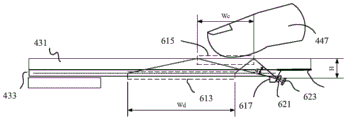
The optical fingerprint sensor module 702 in this particular implementation example is located under the LCD display module 433. One or more illumination sources, such as an illumination source under the LCD display module 433 or/and another one or more illumination sources under the top cover glass 431, are provided for providing illumination or detection light for optical sensing by the optical fingerprint sensor module 702, and may be controlled to emit light to pass at least partially through the LCD display module 433 to illuminate the fingerprint sensing region 615 on the top transparent layer 431 within the device screen area for a user to place a finger therein for fingerprint recognition. Illumination light from one or more illumination light sources may be directed to the fingerprint sensing area 615 on the top surface as if the illumination light were from the fingerprint illumination light zone 613. Another one or more illumination sources may be located below the top cover glass 431 and may be placed adjacent the fingerprint sensing area 615 on the top surface to direct the generated illumination to the top cover glass 431 without passing through the LCD display module 433. In some designs, one or more illumination sources may be located below the bottom surface of the top cover glass 431 to direct the generated illumination to the fingerprint sensing area above the top surface of the top cover glass 431 without having to pass through the LCD display module 433, e.g., to directly illuminate a finger above the top cover glass 431.
As shown in fig. 4B, finger 445 is placed in illuminated fingerprint sensing region 615, with fingerprint sensing region 615 acting as an effective sensing region for fingerprint sensing. A portion of the reflected or scattered light in the fingerprint sensing region 615 is directed into the optical fingerprint sensor module under the LCD display module 433, and a photodetector sensing array within the optical fingerprint sensor module receives this light and collects fingerprint pattern information carried by the received light. The one or more illumination sources are distinct from and operate independent of the backlight of the LCD display module.
In such designs that use one or more illumination light sources to provide illumination light for optical fingerprint sensing, in some implementations, each illumination light source may be controlled to turn on intermittently at a relatively slow period, thereby reducing power for optical sensing operations. In some implementations, the fingerprint sensing operation can be implemented in a two-step process: first, one or more illumination light sources are turned on in a flash mode without turning on the LCD display panel, thereby sensing whether a finger touches the fingerprint sensing region 615 using a flickering light, and then, upon detecting a touch in the fingerprint sensing region 615, the optical sensing module is operated to perform fingerprint sensing based on optical sensing and the LCD display panel may be turned on.
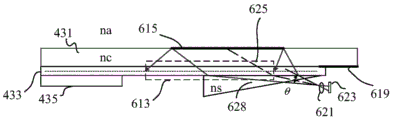
In the example of FIG. 4B, the underscreen optical fingerprint sensor module includes an optically transparent block 701 coupled to the display panel to receive return light from the top surface of the device components; and an optical fingerprint sensor module 702 that performs optical imaging and image acquisition. In designs where the illumination light sources are positioned to direct illumination light first through the top cover glass 431 to the finger, after light from one or more illumination light sources reaches the top cover surface, e.g., at the top cover surface at the fingerprint sensing area 615, the user's finger touches or is positioned without contacting the top cover surface, reflecting or scattering back from the top cover surface. When a fingerprint ridge is in contact with the top surface of the cover plate in the fingerprint sensing area 615, the light reflection under the fingerprint ridge is different from the light reflection under the fingerprint valley at another location where there is no skin or tissue of the finger due to the presence of skin or tissue of the finger in contact at that location. This difference in light reflection conditions at the locations of the ridges and valleys in the area touched by the finger on the top surface of the cover sheet forms an image representing the image or spatial distribution of the ridges and valleys of the touched portion of the finger. The reflected light is directed back to the LCD display module 433 and, after passing through the aperture of the LCD display module 433, reaches the interface of the low index optically transparent block 701 of the optical fingerprint sensor module. The low-index optically transparent block 701 is configured to have a refractive index smaller than that of the LCD display panel so that return light can be extracted from the LCD display panel into the optically transparent block 701. Once the return light is received within the optically transparent block 701, this received light enters the optical imaging unit as part of the optical fingerprint sensor module 702 and is either sensed by the photo detectors within the optical fingerprint sensor module 702 or on the optical sensing array. The difference in light reflection between the ridges and valleys of the fingerprint causes a contrast in the fingerprint image. As shown in FIG. 4B, a control circuit 704 (e.g., a microcontroller or MCU) is coupled to the optical fingerprint sensor module 702 and other circuitry such as a device main processor 705 on the main circuit board.
In this particular example, the optical light path design is configured such that the illumination light enters the cover plate top surface at a total reflection angle on the top surface between the substrate and air interface, and therefore, the imaging optics and imaging sensor array in the optical fingerprint sensor module 702 are collected most efficiently. In this design, the image of the fingerprint ridge/valley area exhibits maximum contrast due to the total internal reflection condition at each finger valley location where the finger tissue does not touch the top cover glass 431 top cover glass surface. Implementations of such imaging systems may have undesirable optical distortions that adversely affect fingerprint sensing. Thus, based on the optical distortion at the optical sensor array along the optical path of the returning light, the acquired image may also be corrected by distortion correction during imaging reconstruction when processing the output signals of the optical sensor array in the optical fingerprint sensor module 702. By scanning the test image pattern of one row of pixels at a time over the entire sensing area of the X-direction lines and the Y-direction lines, distortion correction coefficients may be generated from the image acquired at each photodetector pixel. This correction process may also use the image resulting from tuning a single pixel at a time and scanning the entire image area of the photodetector array. This correction factor only needs to be generated once after assembly of the sensor.
Ambient light from the environment (e.g., sunlight or indoor illumination) may enter the image sensor through the top surface of the LCD panel and then through the aperture in the LCD display module 433. Such background light may produce a background baseline in the valuable image from the finger and thus may undesirably reduce the contrast of the acquired image. Different approaches may be used to reduce this undesirable baseline intensity caused by background light. One example is to turn the illumination source on and off at an illumination modulation frequency f, and the image sensor can acquire the received image at the same illumination modulation frequency by phase synchronizing the source drive pulses with the image sensor frame. In this operation, only one of the image phases contains light from the light source. In implementing this technique, the imaging acquisition can be timed to acquire images with illumination turned on at even (or odd) frames while the illumination is turned off at odd (or even) frames, so the even frames can be subtracted by the odd frames for obtaining images formed primarily of light emitted by the modulated illumination source with significantly reduced background light. Based on this design, one frame of fingerprint signal is generated per display scan frame, and two consecutive signal frames are obtained by turning the illumination light on in one frame and off in the other frame. Subtraction of adjacent frames may be used to minimize or substantially reduce the effects of ambient background light. In some implementations, the fingerprint sensing frame rate may be half of the display frame rate.
In the example shown in fig. 4B, a portion of the light from the one or more illumination sources may also pass through the cover top surface and into the finger tissue. This portion of the illumination light is scattered around, and a portion of this scattered light may eventually be collected by the imaging sensor array in the optical fingerprint sensor module 702. The light intensity of this scattered light is a result of interaction with the internal tissue of the finger and therefore depends on the skin colour of the finger, the finger tissue or the blood concentration in the internal finger tissue. This information of the finger is carried by this scattered light on the finger, is useful for fingerprint sensing, and can be detected as part of the fingerprint sensing operation. For example, the intensity of the user's finger image area may be integrated in the detection for measuring or observing an increase or decrease of the blood concentration related to or dependent on the phase of the user's heartbeat. Such features may be used to determine the heart rate of a user, to determine whether a user's finger is a live finger, or to provide a spoofing device with a counterfeit fingerprint pattern. The latter part of this patent document provides an additional example of information in light using internal tissue information carrying fingers.
In some designs, one or more of the illumination sources in fig. 4B may be designed to emit illumination light of different colors or wavelengths, and the optical fingerprint sensor module may collect return light from the human finger at different colors or wavelengths. By recording the intensity of the respective measured return light at different colors or wavelengths, information associated with the user's skin tone, blood flow within the finger, or internal tissue structures may be measured or determined. For example, when a user registers a finger for fingerprint authentication operations, the optical fingerprint sensor may also be operable to measure the intensity of scattered light from the finger at two different colors or wavelengths of illumination light associated with light color a and light color B, respectively, as intensities Ia and Ib, respectively. When a user's finger is placed on the sensing area on the top sensing surface to measure the fingerprint, the ratio of Ia/Ib can be recorded for comparison with later measurements. The method may be used as part of an anti-spoofing system for a device to reject spoofed devices made by using fingerprints that are analog or identical to the user's fingerprint but that may not match the user's skin tone or other biometric information.
The one or more illumination sources may be controlled by the same control circuitry 704 (e.g., MCU) used to control the image sensor array in the optical fingerprint sensor module 702. The one or more illumination light sources may be pulsed for short periods of time (e.g., low duty cycle) to intermittently emit light and provide pulsed light for image sensing. The image sensor array may be operable to monitor the light pattern at the same pulse duty cycle. If a human finger touches the fingerprint sensing area 615 on the screen, the image acquired at the imaging sensing array in the optical fingerprint sensor module 702 may be used to detect a touch event. The control electronics or MCU 704 connected to the image sensor array in the optical fingerprint sensor module 702 may be operable to determine whether the touch is a human finger touch. If a human finger touch event is determined, MCU 704 may be operative to wake up the smartphone system, turn on one or more illumination sources for performing optical fingerprint sensing, and acquire a complete fingerprint image using the normal mode. The image sensor array in the optical fingerprint sensor module 702 sends the acquired fingerprint image to the smartphone host processor 705, and the smartphone host processor 705 may be operable to match the acquired fingerprint image with a registered fingerprint database. If there is a match, the smartphone unlocks the handset to allow the user to access the handset and initiate normal operations. And if the collected images are not matched, the smart phone feeds back the authentication failure to the user and keeps the locking state of the smart phone. The user may attempt to perform fingerprint sensing again or may enter a password as an alternative to unlocking the handset.
In the example shown in fig. 4A and 4B, the off-screen optical fingerprint sensor module optically images the fingerprint pattern of a touching finger in contact with the top surface of the display screen onto the photodetector sensing array using an optically transparent block 701 and an optical fingerprint sensor module 702 having a photodetector sensing array. By way of example, an optical imaging or detection axis 625 from the fingerprint sensing region 615 to the photodetector array in the optical fingerprint sensor module 702 is shown in FIG. 4B. The optically transparent block 701 and the front end in front of the photo detector sensing array of the optical fingerprint sensor module 702 form a large imaging module to enable suitable imaging for optical fingerprint sensing. Due to optical distortion during this imaging process, distortion correction can be used to achieve the desired imaging operation.
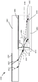
In the optical sensing disclosed herein by the underscreen optical fingerprint sensor module in fig. 4A and 4B and other designs, the optical signal from the fingerprint sensing region 615 on the top transparent layer 431 to the underscreen optical fingerprint sensor module includes different optical components. Fig. 5A-5C illustrate signal generation for light returning from fingerprint sensing region 615 under different optical conditions in order to understand the operation of the off-screen optical fingerprint sensor module. Light entering the finger from the illumination source or from other sources (e.g., background light) may produce internally scattered light in the tissue below the surface of the finger, such as scattered light 191 in fig. 5A-5C. This internally scattered light in the tissue below the finger surface may propagate through the internal tissue of the finger and then through the finger skin into the top transparent layer 431 carrying some information not carried by the light scattered, refracted or reflected by the finger surface, e.g., information about the color of the finger skin, blood concentration or flow characteristics within the finger, or the optical transmission pattern of the finger, including (1) a two-dimensional spatial pattern of external ridges and valleys of the fingerprint; and (2) an internal fingerprint pattern associated with an internal finger anatomy that produces the external ridges and valleys of the finger.
FIG. 5A shows an example of how illumination light from one or more illumination light sources propagates through the LCD display module 433 and generates different return light signals to the underscreen optical fingerprint sensor module after passing through the top transparent layer 431, including light signals carrying fingerprint pattern information. For simplicity, the two illumination rays 80 and 82 at two different locations are directed to the top transparent layer 431 without undergoing total reflection at the junction with the top transparent layer 431. Specifically, illumination rays 80 and 82 are perpendicular or near perpendicular to top layer 431. Finger tissue 60 is in contact with fingerprint sensing region 615 on top transparent layer 431. As shown, the illumination beam 80, after passing through the top transparent layer 431, reaches the finger ridge in contact with the top transparent layer 431 to generate a beam 183 in the finger tissue and another beam 101 that returns to the LCD display module 433. The illuminating light beam 82, after passing through the top transparent layer 431, reaches the finger valley above the top transparent layer 431 to generate a reflected light beam 185 returning from the interface of the top transparent layer 431 to the LCD display module 433, a second light beam 189 entering the finger tissue, and a third light beam 187 reflected by the finger valley.
In the example of fig. 5A, it is assumed that the equivalent index of refraction of the finger skin at 550nm is about 1.44, and the cover glass index of refraction of the top transparent layer 431 is about 1.51. The finger ridge-cover glass interface reflects a portion of the light beam 80 as reflected light 101 to the bottom layer 524 below the LCD display module 433. In some LCD panels, the reflectivity is low, for example, about 0.1%. Most of the light in beam 80 becomes transmitted through beam 183 in finger tissue 60, and finger tissue 60 causes scattering of light 183, producing scattered light 191 that returns to LCD display module 433 and bottom layer 524. Scattering of transmitted light beam 189 from LCD pixel 73 in the finger tissue also contributes to the returning scattered light 191.
The light beam 82 at the finger skin valley location 63 is reflected by the cover glass surface. In some designs, for example, the reflectivity may be about 3.5% as the reflected light 185 is directed toward the bottom layer 524, and the finger valley surface may reflect about 3.3% of the incident light power (light 187) to the bottom layer 524, such that total reflection may be about 6.8%. Most of the light 189 is transmitted into the finger tissue 60. A portion of the optical power in the transmitted light 189 in the finger tissue is scattered by the finger tissue, contributing to the scattered light 191 toward and into the bottom layer 524.
Thus, in the example of fig. 5A, the light reflections from the various interfaces or surfaces at the finger valleys and finger ridges of the touching finger are different, the reflectance difference carries the fingerprint map information, and can be measured to extract the fingerprint pattern of the portion in contact with the top transparent layer 431 and illuminated by the LCD light.
Fig. 5B and 5C show the light paths of two additional types of illumination rays at the top surface under different conditions and at different positions relative to the valleys or ridges of the finger, including the light path at the junction with the top transparent layer 431 under total reflection conditions. The illustrated illumination light generates different return light signals, including light signals that carry fingerprint pattern information to the off-screen optical fingerprint sensor module. It is assumed that the top transparent layer 431 and the LCD display module 433 are bonded together without any air gap therebetween, so that illumination light having a large angle of incidence to the top transparent layer 431 is totally reflected at the cover glass-air interface. Fig. 5A, 5B and 5C show examples of three different sets of diverging beams: (1) the central light beam 82, having a small angle of incidence to the top transparent layer 431 and no total reflection (fig. 5A), (2) the high contrast light beams 201, 202, 211, and 212, being totally reflected at the cover glass 431 when the cover glass surface is not touched and can be coupled into the finger tissue when the finger touches the top transparent layer 431 (fig. 5B and 5C), and (3) the escape light beam having a large angle of incidence, being totally reflected at the top transparent layer 431 even at the position where the finger tissue touches.
For the center beam 82, in some designs, the cover glass surface reflects about 0.1% to about 3.5% of the light to the beam 185, which is transmitted into the bottom layer 524, and the finger skin may reflect about 0.1% to about 3.3% of the light to the beam 187, which is also transmitted into the bottom layer 524. The difference in reflection depends on whether the light beam 82 meets the finger skin ridge 61 or valley 63. The remaining light beam 189 is coupled into finger tissue 60.
For high contrast light beams 201 and 202 that satisfy the condition of local total internal reflection, the cover glass surface reflects almost 100% to light beams 205 and 206, respectively, if the cover glass surface is not touched. When the finger skin ridge touches the cover glass surface and at the location of beams 201 and 202, a large portion of the optical power may be coupled into finger tissue 60 by beams 203 and 204.
For high contrast light beams 211 and 212 satisfying the condition of local total internal reflection, the cover glass surface reflects almost 100% to light beams 213 and 214, respectively, if the cover glass surface is not touched. When a finger touches the cover glass surface and the finger skin valley happens to be at the location of light beams 211 and 212, no optical power is coupled into the finger tissue 60.
As shown in FIG. 5A, a portion of the illumination light coupled into the finger tissue 60 will be randomly scattered by the internal finger tissue to form low contrast light 191, and a portion of such low contrast light 191 will pass through the LCD display module 433 to the optical fingerprint sensor module. The portion of light collected by the optical fingerprint sensor module contains additional information about the finger's skin color, blood characteristics, and internal tissue structure of the finger associated with the fingerprint. Additional features for using internally scattered light in tissue below the surface of a finger in optical sensing will be explained in later sections of this patent document, such as obtaining an optically transmissive pattern of the finger, including (1) a two-dimensional spatial pattern of outer ridges and valleys of the fingerprint; and (2) an internal fingerprint pattern associated with an internal finger anatomy that produces the external ridges and valleys of the finger.
Thus, in areas illuminated by the high contrast light beam, the finger skin ridges and valleys cause different optical reflections, and the reflection difference pattern carries fingerprint pattern information. High contrast fingerprint signals can be achieved by comparing such differences.
Based on the design shown in fig. 2A and 2B, the disclosed under-screen optical sensing technology can optically acquire fingerprints in various configurations.
For example, the specific implementation of fig. 4B based on optical imaging using a large imaging module of the optical sensing modules may be implemented in various configurations. 6A-6C, 7, 8A-8B, 9, 10A-10B, 11, and 12 illustrate examples of various implementations, additional features, and operations of an off-screen optical fingerprint sensor module design for optical fingerprint sensing.
Fig. 6A-6C illustrate an example of an underscreen optical fingerprint sensor module that is optically imaged based on a lens for capturing a fingerprint from a finger 445 pressing against a display top transparent layer 431. Fig. 6C is an enlarged view of the optical fingerprint sensor module portion shown in fig. 6B. The sub-screen optical fingerprint sensor module shown in fig. 6B is located below the LCD display module 433 and includes an optically transparent spacer 617 connected to a bottom surface of the LCD display module 433 to receive return light from the fingerprint sensing region 615 on a top surface on the top transparent layer 431, and an imaging lens 621 located between the spacer 617 and the photodetector array 623 to image the received return light from the fingerprint sensing region 615 onto the photodetector array 623. Unlike the example of the optical projection imaging system without a lens shown in fig. 4B, the example of the imaging design in fig. 6B uses an imaging lens 621 to acquire a fingerprint image at a photodetector array 623, and image demagnification is achieved by the design of the imaging lens 621. To some extent similar to the imaging system in the example of fig. 4B, the imaging system for the optical fingerprint sensor module in fig. 6B may experience image distortion, and suitable optical correction calibrations may be used to reduce such distortion, such as the distortion correction methods described for the system in fig. 4B.
Similar to the assumptions in fig. 5A-5C, assume that the equivalent refractive index of the finger skin at 550nm is about 1.44, and for the top transparent layer 431, the refractive index of the bare cover glass is about 1.51. When the LCD display module 433 is adhered to the top transparent layer 431 without any air gaps, total internal reflection occurs at large angles equal to or greater than the critical angle of incidence of the interface. The total reflection incident angle is about 41.8 ° if the cover glass top surface is not touched, and about 73.7 ° if the finger skin touches the cover glass top surface. The corresponding difference in total reflection angle is about 31.9 °.
In this design, microlens 621 and photodiode array 623 define a viewing angle θ at which an image of a touching finger in fingerprint sensing region 615 is captured. To detect a desired portion of the cover glass surface in fingerprint sensing region 615, the viewing angle may be appropriately aligned by controlling a physical parameter or configuration. For example, the viewing angle may be aligned to detect total internal reflection of the LCD display assembly. Specifically, a fingerprint sensing region 615 on the cover glass surface is sensed aligned with the viewing angle θ. The effectively sensed fingerprint sensing region 615 may be considered a mirror such that the photodetector array effectively detects an image of the fingerprint illumination light zone 613 in the LCD display that is projected onto the photodetector array by the sensed fingerprint sensing region 615. The photodiode/photodetector array 623 may receive an image of the fingerprint illumination light areas 613 reflected by the sensing cover fingerprint sensing region 615. When a finger touches fingerprint sensing region 615, a portion of the light may couple into the ridge of the fingerprint, which causes the photodetector array to receive light from the ridge location to appear as a darker fingerprint image. Since the geometry of the optical detection path is known, fingerprint image distortions induced in the optical path in the optical fingerprint sensor module can be corrected.
As a specific example, considering that the distance H from the central axis of the detection module to the top surface of the cover glass in fig. 6B is 2mm, this design can directly cover a 5mm fingerprint sensing region 615, which fingerprint sensing region 615 has a width Wc on the cover glass. Adjusting the thickness of spacers 617 may adjust detector position parameter H and may optimize effective sense region width Wc. Since H includes the thicknesses of the top transparent layer 431 and the LCD display module 433, the application design should take these layers into account. The spacers 617, microlenses 621, and photodiode array 623 may be integrated under the color coating 619 on the bottom surface of the top transparent layer 431.
Figure 7 illustrates an example of another design consideration for the optical imaging design of the optical fingerprint sensor module shown in figures 6A-6C by using special spacer 618 in place of spacer 617 in figures 6B-6C to increase the size of fingerprint sensing region 615. The spacer 618 is designed to have a width Ws, a thickness Hs, and a low Refractive Index (RI) ns, and the spacer 618 is located under the LCD display module 433, e.g., attached (e.g., adhered) to the bottom surface of the LCD display module 433. The end faces of the spacers 618 are angled or slanted faces that engage the microlenses 621. This relative position of the spacers and lenses is different from the lenses being located below the spacers 617 in figures 6B-6C. The microlens 621 and the photodiode array 623 are assembled into an optical detection module having a detection angle size θ. The axis 625 bending is detected due to optical refraction at the interface between the spacer 618 and the LCD display module 433 and at the interface between the top transparent layer 431 and air. Local angle of incidence And
And is determined by the refractive indices of the component materials, RI, ns, nc, and na.
If nc is greater than ns, then Is greater than
 Thereby, the sensing width Wc is magnified by refraction. For example, assuming that the equivalent RI of the finger skin is about 1.44 at 550nm and the refractive index RI of the cover glass is about 1.51, the total reflection incident angle is estimated to be about 41.8 ° if the top surface of the cover glass is not touched, and the total reflection angle is about 73.7 ° if the finger skin touches the top surface of the cover glass. The corresponding difference in total reflection angles is about 31.9 °. If the
 spacer 618 is made of the same material as the cover glass, the distance from the center of the detection module to the top surface of the cover glass is 2mm, and if the detection angle θ is 31.9 °, the effective sensing area width Wc is about 5 mm. Corresponding to a local angle of incidence of the central axis of If the material of the
 special spacer 618 has a refractive index ns of about 1.4 and Hs is 1.2mm, the detection module is at Is inclined. The effective sensing area width is increased to greater than 6.5 mm. Under these parameters, the detection angular width in the cover glass is reduced to 19 °. Thus, the imaging system of the optical fingerprint sensor module may be designed with the desire to enlarge the size of the
 fingerprint sensing area 615 on the top transparent layer 431.
When the refractive index RI of a particular spacer 618 is designed to be sufficiently low (e.g., using MgF)2、CaF2Or even air to form spacers), the width Wc of the fingerprint sensing region 615 is no longer limited by the thickness of the top transparent layer 431 and the LCD display module 433. This property provides the desired design flexibility. In principle, the effective sensing area may even be increased to cover the entire display screen if the detection module has sufficient resolution.
Because the disclosed optical sensor technology may be used to provide a large sensing area to capture a pattern, the disclosed underscreen optical fingerprint sensor module may be used to capture and detect not only a pattern of a finger, but also a pattern of a larger size, such as a human palm associated with a person, for user authentication.
Fig. 8A-8B illustrate an example of another design consideration for the optical imaging design of the optical fingerprint sensor module shown in fig. 7, in which the opposing detection angle θ' of the photodetector array in the display screen surface and the distance L between the lens 621 and the spacer 618 are set. Fig. 8A shows a cross-sectional view in a direction perpendicular to the surface of the display screen, and fig. 8B shows a view of the device as seen from the bottom or top of the display screen. A fill material 618c may be used to fill the space between the lens 621 and the photodetector array 623. For example, the fill material 618c may be the same material as the particular spacer 618 or another different material. In some designs, the filler material 618c may be an air space.
Fig. 9 shows another example of an under-screen optical fingerprint sensor module based on the design of fig. 7, wherein one or more illumination light sources 614 are provided to illuminate a fingerprint sensing region 615 for optical fingerprint sensing. The illumination light source 614 may be an extended type or a collimated type of light source such that all points within the fingerprint sensing region 615 are illuminated. The illumination source 614 may be a single element light source or an array of light sources.
10A-10B illustrate an example of an underscreen optical fingerprint sensor module using an optical coupler 628 shaped as a thin wedge to improve optical detection at an optical sensor array 623. Fig. 10A shows a cross-section of a device structure with an off-screen optical fingerprint sensor module for fingerprint sensing, and fig. 10B shows a top view of the device screen. An optical wedge 628 (having an index of refraction ns) is located below the display panel structure to alter the total reflection conditions at the bottom surface of the display panel structure that is engaged by the optical wedge 628 to allow light that passes through the bottom surface to be extracted from the display panel structure. An optical sensor array 623 receives light extracted from the display panel structure from the optical wedge 628, and an optical imaging module 621 is located between the optical wedge 628 and the optical sensor array 623 to image the light from the optical wedge 628 onto the optical sensor array 623. In the example shown, wedge 628 comprises an angled wedge surface facing the optical imaging module and the optical sensing array 623. Also, as shown, there is a free space between wedge 628 and photo imaging module 621.
If the light is totally reflected at the sensing surface of the top transparent layer 431, the reflectivity is 100%, with the highest efficiency. However, if the light is parallel to the cover glass surface, the light is also totally reflected at the LCD bottom surface 433 b. The wedge coupler 628 is used to change the local surface angle so that light can be coupled out for detection at the optical sensor array 623. The provision of the micro-apertures in the LCD display module 433 provides a desired light propagation path for light to travel through the LCD display module 433 for underscreen optical sensing. The actual light transmission efficiency may gradually decrease if the light transmission angle becomes too large or when the TFT layer becomes too thick. When the angle is close to the angle of total reflection, i.e., about 41.8 °, and the cover glass has a refractive index of 1.5, the fingerprint image looks good. Accordingly, the wedge angle of the wedge coupler 628 may be adjusted to several degrees, so that the detection efficiency may be improved or optimized. If a higher refractive index of the cover glass is selected, the total reflection angle becomes smaller. For example, if the cover glass is made of sapphire having a refractive index of about 1.76, the total reflection angle is about 34.62 °. The efficiency of detecting light transmission in the display is also improved. Thus, this design using thin wedges provides higher detection angles than total reflection angles and/or uses high index cover glass materials to improve detection efficiency.
In the underscreen optical fingerprint sensor module designs in FIGS. 6A-6C, 7, 8A-8B, 9, and 10A-10B, the fingerprint sensing area 615 on the top transparent surface is not perpendicular or orthogonal to the detection axis 625 of the optical fingerprint sensor module, such that the image plane of the sensing area is also not perpendicular or orthogonal to the detection axis 625. Accordingly, the plane of the photodetector array 623 may be tilted with respect to the detection axis 625 to enable high quality imaging at the photodetector array 623.
Fig. 11 shows three example configurations of such tilting. Fig. 11(1) shows that the sensing region 615a is inclined and not orthogonal to the detection axis 625. In the particular case shown in (2), the sensing region 615b is aligned on the detection axis 625, and its image plane would also lie on the detection axis 625. In practice, the lens 621 may be partially cut away to simplify packaging. In various implementations, the microlenses 621 may also be transmissive or reflective lenses. For example, a specific method is shown in (3). Sensing region 615c is imaged by imaging mirror 621 a. The photodiode array 623b is aligned to detect a signal.
In the above-described design using lens 621, the effective aperture of lens 621 may be designed to be larger than the aperture of the hole in the LCD display layer, which allows light to pass through the LCD display module for optical fingerprint sensing. Such a design may reduce the undesirable effects of wiring structures and other scattering objects in the LCD display module.
Fig. 12 illustrates an exemplary operation of a fingerprint sensor for reducing or eliminating an undesired contribution of background light in fingerprint sensing. The optical sensor array may be used to acquire various frames, and the acquired frames may be used to perform a difference and average operation between multiple frames to reduce the effect of background light. For example, in frame a, the illumination light source for optical fingerprint sensing is turned on to illuminate the area touched by the finger, and in frame B, the illumination is changed or turned off. The subtraction of the signal of frame a and the signal of frame B may be used in image processing to reduce unwanted background light effects.
Unwanted background light in fingerprint sensing can also be reduced by providing suitable optical filtering in the light path. One or more optical filters may be used to filter ambient light wavelengths, e.g., near infrared IR light and portions of red light, etc. In some implementations, such optical filter coatings can be fabricated on surfaces of optical components, including the display bottom surface, the prism surface, or the sensor surface, among others. For example, a human finger absorbs most of the energy at wavelengths below 580nm, and if one or more optical filters or optical filter coatings can be designed to filter light at wavelengths from 580nm to the infrared, the undesirable contribution of ambient light to optical detection in fingerprint sensing can be greatly reduced.
FIG. 13 illustrates an example of an operational procedure for correcting image distortion in an optical fingerprint sensor module. At step 1301, one or more illumination sources are controlled and operated to emit light in a particular area, and the light emission of such pixels is modulated by the frequency F. At step 1302, an imaging sensor under a display panel is operated to capture images at a frame rate of the same frequency F. In optical fingerprint sensing operations, a finger is placed on top of a display panel cover substrate, and the presence of the finger modulates the intensity of light reflection from the top surface of the display panel cover substrate. An imaging sensor under the display captures a reflected light pattern modulated by the fingerprint. At step 1303, demodulation of the signal from the image sensor is synchronized with frequency F and background filtering is performed. The resulting image reduces the effects of background light and includes the image resulting from the emission of light from the pixels. At step 1304, the acquired image is processed and calibrated to correct for image system distortion. At step 1305, the corrected image is used as a human fingerprint image for user authentication.
The same optical sensor used for capturing the user's fingerprint may also be used to capture scattered light from the illuminated finger, as shown by backscattered light 191 in fig. 5A. The detector signals from the returning scattered light 191 in fig. 5A in the region of interest can be integrated to produce an intensity signal. The intensity variation of the intensity signal is evaluated to determine other parameters than the fingerprint pattern, for example, the heart rate of the user, or the internal topological organization of the finger associated with the external fingerprint pattern.
The fingerprint sensor described above may be attacked by malicious individual hackers who can obtain the fingerprint of an authorized user and copy the stolen fingerprint pattern on a carrier similar to a human finger. Such unauthorized fingerprint patterns may be used on a fingerprint sensor to unlock a target device. Thus, a fingerprint pattern, although a unique biometric identifier, may not be a completely reliable or secure identification by itself. The off-screen optical fingerprint sensor module may also be used as an optical anti-spoofing sensor for sensing whether an input object having a fingerprint pattern is a finger from a living body and for determining whether a fingerprint input is a spoofing attack. This optical anti-spoofing sensing function is provided without the use of a separate optical sensor. Optical anti-spoofing can provide a high speed response without compromising the overall response speed of the fingerprint sensing operation.
Fig. 14 shows exemplary extinction coefficients of monitored materials in blood, the optical absorption in blood differing between the visible spectral range of red light, e.g., 660nm, and the infrared range of IR light, e.g., 940 nm. By illuminating the finger with probe light at a first visible wavelength (color a) and a second, different wavelength (color B), such as an Infrared (IR) wavelength, differences in optical absorption of the input object can be collected to determine whether the touch object is from a live finger. One or more illumination light sources for providing optical sensing illumination may be used to emit light of different colors and as probe or illumination light of at least two different wavelengths of light for live finger detection using different optical absorption behavior of blood. When a person's heart beats, the pulse pressure pumps blood to flow in the artery, so the extinction ratio of the monitored material in the blood changes with the pulse. The received signal carries a pulse signal. These properties of blood can be used to detect whether the material being monitored is a live or false fingerprint.
Fig. 15 shows a comparison between the behavior of optical signals in reflected light from an inanimate material such as a fake finger or a spoof device having a fake fingerprint pattern and a live finger. The optical fingerprint sensor may also operate as a heartbeat sensor to monitor living subjects. When two or more wavelengths of probe light are detected, the difference in extinction ratios can be used to quickly determine whether the material being monitored is a living object, such as a living fingerprint. In the example shown in fig. 15, different wavelengths of probe light are used, one visible wavelength and the other infrared IR wavelength as shown in fig. 14.
When an inanimate material touches the top cover glass over the fingerprint sensor module, the received signal reveals an intensity level associated with the surface pattern of the inanimate material, and the received signal contains no signal components associated with a live finger. However, when a live finger touches the top cover glass, the received signal reveals signal characteristics associated with the live subject, including significantly different intensity levels, due to the different extinction ratios at the different wavelengths. This method does not take a long time to determine whether the touch material is a part of a living body. In fig. 15, the pulse-like signal reflects multiple touches, rather than blood pulsations. Multiple touches similar to inanimate material do not show differences caused by live fingers.
Such optical sensing of different optical absorption behavior of blood at different optical wavelengths may be performed in short periods for live finger detection and may be faster than optical detection of a heartbeat of a person using the same optical sensor.
In the LCD display, the LCD backlight illumination is white light, containing light in the visible spectral range and the infrared IR spectral range that performs the above-described live finger detection at the optical fingerprint sensor module. An LCD filter in the LCD display module may be used to allow the optical fingerprint sensor module to obtain the measurements in fig. 14 and 15. In addition, a designated light source for generating optically sensed illumination light may be operated to emit detection light at selected visible and infrared IR wavelengths at different times, and the two different wavelengths of reflected detection light are collected by the optical detector array 623 to determine whether the touch object is a live finger based on the above-described operations shown in fig. 14 and 15. It should be noted that although the reflected detection light of the selected visible and IR wavelengths at different times may reflect different optical absorption characteristics of blood, the fingerprint image is always acquired at different times by the detection light of the selected visible wavelength and the detection light of the infrared IR wavelength. Thus, fingerprint sensing can be performed at visible and infrared IR wavelengths.
Fig. 16 shows an example of an operation procedure for determining whether a target in contact with an LCD display screen is part of a live finger by operating one or more illumination light sources for optical sensing to illuminate the finger with two different colors of light.
As another example, the disclosed optical sensor technology can be used to detect whether a captured or detected pattern of a fingerprint or palm is from a live human hand by a "live finger" detection mechanism through mechanisms other than the different optical absorption of blood at different optical wavelengths described above. For example, a living finger is typically moved or stretched due to natural movement or motion (intentional or unintentional) of a person, or is typically pulsed when blood flows through a body associated with a heartbeat. In one implementation, the optical fingerprint sensor module may detect changes in return light from the finger or palm due to heartbeat/blood flow changes, thereby detecting whether a live heartbeat is present in an object appearing as a finger or palm. User authentication may enhance access control based on a combination of optical sensing of a fingerprint/palm pattern and positive determination of the presence of a living body. As another example, when a person touches the LCD display screen, changes in the touch force may be reflected in one or more ways, including fingerprint pattern distortion, changes in the contact area between the finger and the screen surface, widening of fingerprint ridges, or dynamic changes in blood flow. These and other variations can be measured by optical sensing based on the disclosed optical sensor technology and can be used to calculate touch force. Such touch force sensing may be used to add more functionality to the optical fingerprint sensor module than fingerprint sensing.
In the above example, as shown in fig. 4B and 6B, the fingerprint pattern is captured on the optical sensor array via the imaging module, optical distortion typically reduces image sensing fidelity. This image distortion can be corrected in various ways. For example, an optical image may be generated at the optical sensor array using a known pattern, and image coordinates in the known pattern may be correlated with the optical image generated at the optical sensor array with distortion for calibrating an imaging sensing signal output by the optical sensor array for fingerprint sensing. The fingerprint sensing module calibrates the output coordinates with reference to an image of the standard pattern.
Various implementations of the disclosed optical fingerprint sensor module may be made in accordance with the disclosure in this patent document.
For example, the display panel may be configured to: each of which can be controlled individually; the display panel includes an at least partially transparent substrate and a substantially transparent cover substrate. The optical fingerprint sensor module is located under the display panel for sensing an image formed on top of a surface of the display panel. The optical fingerprint sensor module may be used to sense an image formed by light emitted from the display panel pixels. The optical fingerprint sensor module may include a transparent block having a refractive index lower than that of the display panel substrate, an imaging sensor block having an imaging sensor array, and an optical imaging lens. In some implementations, the low index block has a refractive index in a range of 1.35 to 1.46 or 1 to 1.35.
As another example, a method for fingerprint sensing may be provided, wherein light emitted from a display panel is reflected by a cover substrate, and a finger on top of the cover substrate interacts with the light to modulate a light reflection pattern of a fingerprint. The imaging sensing module below the display panel is used for sensing the reflected light pattern image and reconstructing a fingerprint image. In one implementation, the emitted light from the display panel is modulated in the time domain, and the imaging sensor is synchronized with the modulation of the emitting pixels, where the demodulation process rejects most of the background light (not the light from the target pixels).
And III, a lens-pinhole imaging design for optical sensing under the display.
In various implementations of the off-screen optical fingerprint sensor module technology for fingerprint sensing disclosed herein, an imaging module having at least one imaging lens may be used to enable optical imaging of an illuminated touch portion of a finger onto an optical sensor array in an off-screen optical fingerprint sensor module. The lens effect of the imaging module is used to some extent to control the spatial spread of the return light, which can compete spatially at the optical sensor array for return light from different locations on the touch portion of the finger, so that the imaging lens can maintain the desired spatial imaging resolution of the spatial information of the return light corresponding to the fingerprint pattern on the finger as it directs the return light to the optical sensor array. The spatial imaging resolution of an imaging module having a single imaging lens or an assembly of two or more imaging lenses is proportional to the numerical aperture of the imaging module. Therefore, a high-resolution imaging lens requires a large numerical aperture, and therefore a lens having a large diameter is required. This aspect of the lens-based imaging module inevitably requires a large lens system to produce a high resolution imaging system. In addition, a given imaging lens has a limited field of view that increases with decreasing focal length and decreases with increasing focal length.
In many fingerprint sensing applications, such as optical fingerprint sensors implemented under a display screen in a mobile device, it is desirable to incorporate a compact imaging system with high spatial imaging resolution and a large field of view. In view of the above-described trade-off of various imaging features of lens-based imaging systems, the following provides a compact optical imaging system for optical fingerprint sensing by combining lenses and pinholes into a lens-pinhole imaging system, wherein the lenses are used to form the lens-based imaging system to achieve high spatial imaging resolution and reduced size images acquired at an optical detector array through the lenses to reduce the size of the optical detector array through the same lenses, and placing pinholes in front of the lenses to produce a large field of view in the optical imaging by implementing a pinhole camera without the need for large diameter lenses. Conventional pinhole cameras may include a small aperture for optical imaging and may produce a large field of view while suffering from limited image brightness due to the small aperture and low spatial imaging resolution. When properly designed, the combination of an imaging lens and a pinhole camera can benefit from the high spatial imaging resolution of the imaging lens and the large field of view of the pinhole camera.
FIG. 17 illustrates an example of an optical fingerprint sensor module 4620 placed under an LCD display screen where a pinhole and lens are used to form an optical imaging system for the optical fingerprint sensor module 4620. One or more illumination sources are disposed at locations below the LCD display module 433 to generate illumination light to pass through the LCD display module 433 and the top transparent layer 431, the top transparent layer 431 including a fingerprint sensing region 615 on a top surface of the transparent layer 431. One or more illumination sources 4661 are disposed below top transparent layer 431 to generate illumination light to fingerprint sensing region 615 on the top surface of transparent layer 431. One or more illumination light sources may be located in or beside the optical fingerprint sensor module 4620 to provide, in addition to illumination for fingerprint sensing, a breathing light indicator for indicating that optical fingerprint sensing is ongoing or that the optical fingerprint sensor module 4620 is turned on or activated.
In the example shown in fig. 17, optical sensing module 4620 is a compact module using microlenses 4621e, which microlenses 4621e may have a small diameter approximately the same size as the pinholes, and thus be slightly larger than the pinholes. The microlenses 4621e are joined to pinhole structures 4621g, which are optically opaque and may be a layer of blackened or metallic material formed on the surface of a pinhole substrate 4621f made of an optically transparent material, and have openings as pinholes 4643. A microlens 4621e is placed on the underside of the pinhole substrate 4621 f. In operation, the optical layer above the pinholes 4643 in the pinhole structure 4621g is configured to create a large optical field of view when collecting return light from the LCD display panel and transmit the collected light towards the optical sensor array 4623 e. Optical detectors in optical sensor array 4623e generate detector signals in response to the received optical pattern, and detector circuitry block 4623f is coupled to optical sensor array 4623e to receive and process the detector signals. In some implementations, the detector circuit block 4623f may include a flexible printed circuit (PFC). Microlens 4621e receives light transmitted from the pinhole and focuses the received light onto optical sensor array 4623e for optical imaging at optical sensor array 4623e with enhanced spatial imaging resolution, as compared to the lower spatial imaging resolution of the pinhole when light is projected onto optical sensor array 4623e without microlens 4621 e. In this design, the low resolution of the pinholes is compensated for by using microlenses 4621e, and the limited field of view of microlenses 4621e is compensated for by the large field of view of the assembly of low index of refraction layer 4618e, high index of refraction layer 4621f, and pinholes 4643.
In the example shown in fig. 17 using a pinhole-lens assembly for optical imaging, the object plane of the pinhole-lens assembly is proximate to fingerprint sensing region 615 on the top surface of top transparent layer 431, such as a cover glass for a touch sensing LCD display panel, and the imaging plane of the pinhole-lens assembly is the receiving surface of the optical detector of optical sensor array 4623 e. In addition to the pinhole substrate 4621f, an optically transparent spacer 4618e having a lower refractive index than the pinhole substrate 4621f is provided between the pinhole substrate 4621f and the LCD display panel. The use of a lower index material over the pinhole substrate 4621f is part of the optical design to achieve a large field of view for receiving light from the LCD display panel. In some implementations, the lower index spacer 4618e may be an air gap. This design provides an optical interface between the lower index spacer 4618e and the higher index pinhole substrate 4621f with two different optical materials, and optical refraction at this interface converts the large field of view (FOV) of incident light from the LCD display panel in the lower index spacer 4618e (e.g., in some cases, about 140 degrees) to a smaller FOV in the higher index pinhole substrate 4621 f. Thus, the output light rays produced by the pinhole-lens assembly have a relatively small FOV.
This reduced FOV design is advantageous in several respects. First, the optical input FOV in the lower index spacer 4618e of the optical fingerprint sensor module 4620 is such that the input has a large FOV. Second, the actual FOV processed by the pinhole-lens assembly located below the higher index pinhole substrate 4621f is a reduced FOV relative to the optical input FOV, such that rays with large angles of incidence are limited to this reduced FOV. This is beneficial because such a reduced FOV reduces image distortion caused by rays in large angles of incidence at the pinhole-lens assembly. Furthermore, this reduced FOV at the pinhole-lens assembly reduces unwanted pinhole shadowing effects that distort the brightness distribution of the image at the optical sensor array.
Unlike conventional pinhole cameras that use pinholes of about 40 microns in diameter in some pinhole camera designs, the pinholes 4643 formed in the opaque layer 4621g are designed to have a diameter much larger than the typical size of pinholes in pinhole cameras, in some designs, for example, greater than 100 microns, or 200 microns (e.g., 250 microns). In this combination of lenses and pinholes, the use of a high index of refraction material for the pinhole substrate 4612f over the pinhole 4643, and the use of a low index of refraction layer 4618e over the pinhole substrate 4612f allow the pinhole 4643 to have a diameter much larger than the typical size of a pinhole in a pinhole camera, while still achieving a large FOV. For example, in some implementations, when the lens 4621e is configured as a hemispherical lens, with a flat surface facing the pinhole 4643 and a partially spherical surface that directs light from the pinhole 4643 to the photodetector array 4621e, the diameter of the pinhole 4643 may be substantially the same as or similar to the radius of curvature of the curved surface of the lens 4621 e.
Additional design features may also be implemented to improve the overall optical performance and compactness of pinhole-lens assembly based optical imaging systems. For example, as shown in fig. 17, an additional optical layer may be placed between the lens-pinhole assembly and the photodiode array 4623 e. In this example, optically transparent spacer 4621h and protective material 4623g are disposed in the optical path from the pinhole-lens assembly to optical sensor array 4623 e. In some implementations, spacer 4621h may be a low index layer, such as an air gap or the like, and protective material 4623g may be a layer covering the tops of the optical detectors of optical sensor array 4623e and having a refractive index higher than the refractive index of spacer 4621 h. Layers 4621h and 4623g may be configured to reduce or eliminate imaging distortion at optical sensor array 4623 e. When light is refracted at the medium interface, there is a non-linearity in the direction of the refracted rays and image distortion occurs at optical sensor array 4623 e. This distortion becomes more pronounced when the angle of incidence is large. To reduce such distortion, the optical thickness ratio of spacers 4621h and 4623g may be selected according to the optical structure of the pinhole-lens assembly and the optical objective field of view of the pinhole-lens assembly (e.g., the optical layer from the top sensing surface of top transparent layer 431 to pinhole substrate 4621 f).
Optical distortion occurs at each interface with a different optical material in the optical path of light along the top of the LCD display panel to optical sensor array 4623 e. One design technique for reducing this optical distortion is: an optical matching structure (i.e., an optical layer on the imaging side of the pinhole-lens assembly) is provided on the underside of the pinhole-lens assembly to correspond to the optical structure on the upper side of the pinhole-lens assembly (i.e., an optical layer on the object side of the pinhole-lens assembly) such that optical distortion occurring along one interface in the optical path of the LCD panel to the pinhole-lens assembly in the object side of the pinhole-lens assembly is cancelled or compensated for by optical refraction at the matching interface in the optical path of the pinhole-lens assembly to optical sensor array 4623e along the pinhole-lens assembly in the imaging side of the pinhole-lens assembly. The optical matching layer on the imaging side of the pinhole-lens assembly is designed by taking into account the optical power of the lenses in the pinhole-lens assembly. In a pinhole imaging system having only a pinhole 4643 and no lens 4621e, there is optical distortion when the medium does not match between the object field and the image field. When the FOV is large, the distortion, which may be in the form of barrel distortion, is tested by using a grid pattern placed on the top sensing surface. Barrel distortion caused by mismatched optical layers between the object field and the image field of pinhole 4643 is undesirable because they directly affect the accuracy of the fingerprint pattern acquired by optical sensor array 4623 e. It should be noted that the level of such distortion is typically higher in the central portion of the image field than in the peripheral portion at optical sensor array 4623 e.
To mitigate this distortion, the material layers below the needle holes 4643 and lenses 4621e in the image field may be constructed according to their refractive index and thickness values to reverse the distortion introduced by the material layers on the object side. This is achieved by matching the refractive behavior of the large incident angle in order to correct the image to be linearly formed on the detector surface. For example, in a pinhole imaging system with an imaging magnification of 1/5, if there is a 2mm thick glass layer and a 1mm thick air gap layer over pinhole 4643, a 0.4mm thick glass layer and a 0.25mm thick air gap may be placed under pinhole 4643 and over optical sensor array 4623e to reduce optical distortion at optical sensor array 4623 e. This technique may be used to provide a matching layer below the pinholes 4643 for a complex layer of material above the pinholes 4643.
FIG. 18 shows an example of different layers in an LCD display module above an optical fingerprint sensor module. In this embodiment, sensor module 4620 is integrated under an LCD display module. Illumination source 4661 and additional light sources are also integrated in or near sensor module 4620. The virtual button for optical Fingerprint (FP) sensing displayed within the LCD display near the edge is virtual in that it is located on an area of the continuous top surface across the display (no separate physical button for fingerprint sensing) and is the display area indicated as fingerprint sensing area 615 (fig. 17) for fingerprint sensing.
In the example of fig. 18, the materials in the LCD backlight assembly of the LCD display module are designed to provide a light transmission path to allow return probe light from the top sensing region to reach the underlying optical fingerprint sensor module below the LCD display module. Light-transmitting holes or slits can be formed using such a material. To change the appearance of the display at the location of the optical sensor to reduce the visibility of the optical sensor, a diffuser film 4433d may be integrated with a prism 4433c above the backlight waveguide layer 4433f to diffuse light to the LCD pixels for uniform illumination, and an additional diffuser 4433i may be integrated with a mirror film 4433g below the backlight waveguide layer 4433f and reflect or recycle the backlight back to the LCD layer to improve illumination efficiency. In some implementations, the additional diffuser films 4433d and 4433i can be shaped as stripes around the edges of the optical fingerprint sensor module to diffuse the light scattered in the light path such that the edges of the light path around the optical fingerprint sensor module below the LCD display module are hidden or invisible.
Fig. 19 shows an exemplary implementation of the design in fig. 17, where the pinhole layer coating 4621g on the bottom surface of the pinhole substrate 4621f is configured to have a high optical reflection on its upper side facing the pinhole substrate 4621 f. This feature is used to compensate for area reflections of mirror film holes or optical reflector layers or diffuser layers in the LCD layer above the optical fingerprint sensor module 4620.
In some implementations, an additional diffuser layer 4621i may be applied on top of the pinhole substrate 4621f, as shown in fig. 19, to cause optical diffusion, and a central portion of the additional diffuser layer 4621i may include a clear light path to receive return light from the LCD display module for optical sensing.
Further, fig. 19 shows example locations of one or more additional light sources 436a mounted below the additional diffuser layer 4621 i. The light emitted from the additional light source 436a is scattered by the diffuser 4621 i. The additional light source 436a may emit light of different optical wavelengths, including, for example, wavelengths for finger illumination and other wavelengths for other functions, such as a breathing light function, etc.
Fig. 20 shows an example where one or more cover glass lower light sources 4661 are provided to illuminate a touch finger 4447 for optical sensing. Light generated by one or more cover glass lower light sources 4661 is represented by light 4661a and may be transmitted into the finger tissue or transmitted through the stratum corneum of the finger skin. For example, when light 4661a is transmitted through the skin of the finger and through the finger tissue, the light is scattered by the finger tissue. A portion of the scattered light is passed out as signal light 4661b carrying fingerprint information including information on topological internal organizational structures associated with the external fingerprint pattern, and detected by optical fingerprint sensor module 4620. Signal light 4661b is incident on the sensing region on the top glass at a large angle and can collect and carry fingerprint information when the skin is wet or dry. Thus, the use of one or more cover glass lower light sources 4661 may improve the detection performance and reliability of the sensor.
The pinhole-lens assembly for optical imaging in the example of fig. 17 may achieve higher spatial imaging resolution to acquire fine features in the acquired image compared to the spatial imaging resolution of a system having only the pinhole 4643 without the lens 4621 e. This higher spatial imaging resolution is a result of having lens 4621 e. Fig. 21A and 21B illustrate an imaging operation with only a pinhole and an imaging operation of a pinhole-lens assembly.
Referring to fig. 21A, fig. 21A shows a pinhole imaging system without a lens, a pinhole 4643 diffracting an incident beam 4661 to produce a diffracted output beam 4673, the output beam 4673 diverging due to diffraction by the pinhole 4643. Diverging beam 4673 forms an image spot 4679 at imaging plane 4667 that reflects the resolution of the imaging system.
Fig. 21B shows the addition of a microlens 4621e under the pinhole 4643. Due to the combination of the microlens 4621e and the pinhole 4643, the curvature of the microlens 4621e alters the wavefront of the light beam diffracted by the pinhole 4643 to produce a smaller spot 4681 at the imaging plane 4667 than a spot 4679 produced without the lens 4621e but only by the pinhole 4643 alone.
The pinhole-lens assembly may be implemented to provide a compact optical fingerprint sensor module 4620 in the example of fig. 17. Due to refraction at the medium interface, the light propagation angle can be controlled by using different optical materials. For example, as shown in fig. 22, if the index of refraction n1 in the medium above the pinhole substrate 4465 is lower than the index of refraction n2 of the pinhole substrate 4465, the light beam 4683 having a large incident angle is bent into a light beam 4685 having a smaller angle after entering the pinhole substrate 4465. Thus, by using higher index materials for pinhole substrate 4465, an extremely large field of view for receiving input light on the object side of the pinhole-lens assembly may be achieved. In some implementations, a large FOV (e.g., near or above 140 degrees) can be achieved by using a high index material for the pinhole substrate 4465 to create a sufficiently large difference between the indices of refraction of the pinhole substrate 4465 and the layers above the pinhole substrate 4465.
The above-described design for achieving large diffractive bending of light at the top surface of pinhole substrate 4465 may be used to reduce the thickness of an optical fingerprint sensor module by incorporating some low index gap (e.g., air gap) in the light path. In addition, the image uniformity of the image from the pinhole-lens assembly can be improved because the tilt angle of the rays entering the lens below the pinhole aperture plate decreases as the FOV decreases due to the large refraction at the top of the pinhole aperture plate 4465.
In the pinhole-lens assembly, the microlenses are placed under the pinholes 4671, so the optical aperture of the microlenses is small due to the small opening of the pinholes 4671. Thus, the microlens exhibits lower aberrations because the light rays of pinhole 4671 collected by the microlens are generally close to the axis of the microlens's curved surface.
In implementing the pinhole-lens assembly, the center of the pinhole 4671 is located at or near the center of the surface of the microlens 4675. In the example of fig. 22, a hemispherical lens is shown as an example, and is bonded (e.g., glued) to a pinhole plate to achieve this configuration. The plane of the hemispherical lens 4675 faces upward to engage the pinhole 4671, and the center of the plane of the hemispherical lens 4675 is located at or near the center of the pinhole 4671. With this design, incident light having a small or large angle of incidence with the plane of the hemispherical lens 4675 through the pinhole 4671 will have its ray direction coincident with the radial direction of the hemispherical lens 4675, i.e., the optical axis of the lens in the radial direction. This configuration reduces optical aberrations. For light beams 4663 and 4683 having different incident angles on top of the pinhole substrate 4465, their optical paths after entering the pinhole substrate 4465 are changed to approximate the respective optical axes 4689 and 4691 of the hemispherical lens surfaces. Thus, under this particular design, the image spots 4681 and 4693 formed by the light beams 4663 and 4683 exhibit low optical aberration, although having different angles of incidence.
The pinhole-lens assembly suffers from aperture shading effects, which causes the final image at the imaging plane (optical sensor array 4623e) to be brighter at the center and darker in the peripheral regions, and the brightness gradually changes from center to peripheral regions along the radial direction. This effect degrades the image acquired at optical sensor array 4623e, but may be reduced by using corrective optical filtering that changes the spatial brightness distribution. For example, an optical filter having a spatially graded transmission profile may be inserted in the optical path of light received by the optical fingerprint sensor module, e.g., at a location between the OLED display panel and the optical sensor array. The gradient transmission filter is configured to exhibit high optical attenuation at or near the center of the pinhole with reduced optical attenuation radially outward from the center of the pinhole to offset spatial variations in the light intensity distribution of the light caused by the pinhole. Fig. 23 shows an example of an optical attenuation profile of such a gradient transmission filter, which has a radial gradient attenuation decreasing from the center to the edge.
In some implementations, the gradient transmission filter may include one or more coatings that may be made on a surface of the light path to correct for image brightness non-uniformities, such as the bottom surface of the display, the surface of the module component, or the top surface of the optical sensor array. In addition to counteracting spatial non-uniformities caused by aperture shadowing effects, filters may also be used to correct for other types of brightness non-uniformities, and may also include features that may reduce other optical distortions and optical aberrations.
The optical fingerprint sensor module disclosed above using a pinhole-lens assembly for optical imaging onto an optical sensor array may also be used to construct an optical fingerprint sensor module that is positioned under a top glass cover plate and placed next to an LCD display screen under the same top glass cover plate. Such an optical fingerprint sensor module may be placed next to the LCD display screen under the same top glass cover plate to achieve a common and continuous top surface over the LCD display and the optical fingerprint sensor module. Further, several examples are given in section IV entitled "optical fingerprint sensor on one side of LCD display".
IV, invisible optical fingerprint sensor under LCD design.
According to some implementations, to make the optical fingerprint sensor module "invisible" under the display screen, the optical fingerprint sensor module may be placed under an opaque border of the display screen. In many commercially produced LCD screens, an optically opaque border is present on the peripheral side of the LCD screen, such as a peripheral opaque bezel surrounding the central region of the LCD screen. Fig. 24A shows a top view of an LCD display screen in which peripheral opaque bezel 3220 is formed on four sides of the LCD screen and blocks LCD display pixels in border areas on the four sides of the LCD screen so that during display operation, a user can only see central LCD display area 3210 exposed by the openings of peripheral opaque bezel 3220.
Thus, as shown in fig. 24A and 24B, the LCD lower optical fingerprint sensor module may be placed below the LCD screen near or inside the area covered by the peripheral opaque border 3220 such that the portion 3230 of the LCD screen below the peripheral opaque border 3220 above the optical fingerprint sensor module may be altered to provide one or more desired localized transmission features or areas in the LCD screen stack for directing the probe light carrying fingerprint information to the optical fingerprint sensor module.
Fig. 24B shows a cross-sectional view of the different layers under the marked circular area in fig. 24A. An LCD screen portion 3230 having optically transmissive features or areas for directing light to the optical fingerprint sensor module is positioned below the peripheral opaque border 3220, so that when an LCD display image is viewed, the LCD screen portion 3230 is largely invisible to a user because the peripheral opaque border 3220 is above and hides the LCD screen portion 3230 from the user's view. Notably, unlike some other examples of under-LCD optical sensing designs, the center of intra-screen FPS sensing area 615 is spatially offset from the center of LCD screen portion 3230 having an optically transmissive feature or area. Thus, the location of the lower optical fingerprint sensor module is spatially offset from the location of FPS sensing area 615 within the screen because the lower optical fingerprint sensor module is placed under peripheral opaque border 3220, rather than directly under FPS sensing area 615 within the screen.
This design of placing the LCD screen portion 3230 with optically transmissive features or areas partially or completely under the perimeter opaque border 3220 to direct probe light into the optical fingerprint sensor module under the LCD is referred to as an "invisible" optical sensor design. This design may hide the partially transmissive features or areas in LCD screen portion 3230 of the LCD screen stack and the underlying optical fingerprint sensor module from view even when one or more additional illumination lamps 4663 or 4661 are provided for illuminating the area above in-screen FPS sensing area 615 where a user places a finger thereon for optical fingerprint sensing and other optical sensing operations.
With this arrangement, intra-screen FPS sensing area 615 can no longer be placed anywhere within the LCD screen, but rather should be located within the LCD screen near the location of LCD screen portion 3230 having the partially transmissive feature or area, such that a portion of the light from intra-screen FPS sensing area 615 that reaches LCD screen portion 3230 below peripheral opaque border 3220 can be directed through the LCD screen to the underlying optical fingerprint sensor module for optical sensing. In various implementations of this design, the LCD screen portion 3230 with the partially transmissive features or regions is designed to provide one or more light receiving paths (at least partially covered by the peripheral opaque bezel 3220) from the intra-screen FPS sensing area 615 to the under-LCD optical fingerprint sensor module to improve optical detection performance while illumination of the intra-screen FPS sensing area 615 can be achieved independently of this particular design. For example, one or more additional illumination lamps 4663 or 4661 may be placed in desired locations to direct illumination light to the in-screen FPS sensing area 615 without having to pass through the LCD screen portion 3230 having the partially transmissive feature or area to reach the in-screen FPS sensing area 615.
The above-described design of placing LCD screen portion 3230 with partially transmissive features or areas at least partially covered by perimeter opaque border 3220 may be applied to various configurations of optical fingerprint sensor modules under an LCD for implementing the design in fig. 24. For example, in fig. 4B, an under-LCD optical fingerprint sensor module that collects light from the in-screen FPS sensing area 615 using a projector system, or in fig. 6B, 7, 8A, 9 and 10A, an imaging system having a lens located below the LCD screen in the optical path to the optical sensor array to collect probe light from the in-screen FPS sensing area 615 and project the collected probe light into the optical sensor array, or as shown in fig. 17-23, a pinhole and a combination of lenses downstream of the pinhole to receive transmitted probe light from the pinhole and focus the received probe light onto the optical sensor array for optical imaging.
Referring back to fig. 24A-24B, LCD panel portion 3230 having partially transmissive features or areas partially or fully covered by a peripheral opaque border 3220 may be used in various designs to increase the optical transmission of LCD panel portion 3230, as well as to form transmissive apertures or more transmissive areas compared to other portions of the LCD panel. 25A-25C illustrate a specific example in which a peripheral portion of an LCD screen is altered by providing improved optical transmission in a modified LCD screen portion 3230 to form LCD screen portion 3230, where an underlying optical fingerprint sensor module 4620 as shown uses the pinhole and lens combination shown in FIG. 17 to collect light for an optical sensor array.
In a design example, as shown in fig. 25A and 25B, the under-LCD optical fingerprint sensor module forms an optical system using both pinholes 4643 and microlenses 4621e together to collect light from the FPS sensing area 615 on the top transparent layer 431 and direct the collected light to an optical sensor array 4623e in the optical fingerprint sensor module 4620 to achieve a large field of view and high imaging resolution. For more details, see fig. 17-23 and related description. Spacers 4621h may be a layer of low refractive index material, such as an air gap, and protective layer 4623g may be a bandpass filter. Fig. 25B shows one or more cover glass down additional illumination sources 4661 positioned to illuminate a finger to be detected and generate probe light in the optical path from the in-screen FPS sensing area 615 to the LCD screen portion 3230 to the fingerprint sensor module. Additional light sources 4663 may be placed near the optical fingerprint sensor module 4620 or just above the optical fingerprint sensor module 4620 to provide localized illumination for finger illumination. These light sources may also be used as breathing lights to indicate the operational status of the optical fingerprint sensor module. As further explained in the following sections, other light sources, such as ambient light sources, may also be used as detection light sources for optical sensing.
25A-25C illustrate altering the peripheral portion of the LCD screen by peeling off a small portion of LCD prism and diffuser films 4433C and 4433e and other layers underneath LCD prism and diffuser films 4433C and 4433e to form LCD screen portion 3230. Peripheral portions of the LCD prism and diffuser films 4433c and 4433e are removed to create voids for optical transmission, thereby forming modified LCD prisms and diffuser films 5433c and 5433e as shown in fig. 25A. The void is used to insert an optical coupler 5617 under the LCD layer 4433b and over the backlight waveguide layer 4433 f. The optical coupler 5617 may be implemented as a wedge-shaped optical coupler with a tapered wedge-shaped portion to extend into the space between the stripped and modified LCD prism and diffuser films 5433c and 5433e, and the tapered wedge-shaped portion may reach the LCD screen area 3100 not covered by the perimeter opaque bezel 3220 as an optical path to better collect light from the intra-screen FPS sensing area 615. Accordingly, optical coupler 5617 includes a top coupler portion that receives light from in-screen FPS sensing area 615 and sends the received light from in-screen FPS sensing area 615 along a slanted optical path to an area under peripheral opaque border 3220, wherein hidden optical fingerprint sensor module 4620 is positioned to collect the received light from in-screen FPS sensing area 615 for optical sensing. This feature of optical coupler 5617 affects only a small area of the LCD screen near the peripheral opaque border 3220 so that the impact on display quality is insignificant. A thin spacer 5617a is formed between the bottom surface of LCD layer 4433b and the top surface of optical coupler 5617 and may be, for example, a soft, optically clear or transparent adhesive layer. Thus, probe light from the intra-screen FPS sensing region 615 passes through the thin spacer 5617a, and is further collected and guided by the optical coupler 5617 into the backlight waveguide layer 4433 f.
In other implementations, the peripheral portion of the LCD screen is separated or peeled away from a short section of the LCD prism and diffuser films 4433c and 4433e and other layers underneath the LCD prism and diffuser films 4433c and 4433e to create a void for light transmission for insertion of the optical fingerprint sensor module. For example, the backlight module of the LCD display panel structure includes a peripheral region within an area at least partially covered by the peripheral border and separated from other portions of the LCD display panel structure to provide a location for the optical fingerprint sensor module to be positioned below the peripheral opaque border.
Another modification to the stripped LCD peripheral portion is to remove a small perimeter portion of the optical reflector film layer 4433g as a modified optical reflector film layer 5433g to expose the bottom surface of the backlight waveguide layer 4433f for placement of the optical fingerprint sensor module 4620. In this example, the top surface of the optical fingerprint sensor module 4620 is a pinhole substrate 4621f that is placed against the bottom surface of the backlight waveguide layer 4433f to receive light directed by the optical coupler 5617. In this example, the optical path from the intra-screen FPS sensing region 615, through the top transparent layer 431, through the touch sensing layer 4433a, the LCD layer 4433b, the spacers 5617a, the optical coupler 5617, and the backlight waveguide layer 4433f into the optical fingerprint sensor module 4620 does not include an air gap. In other implementations, an air gap may be present in the optical path described above.
Fig. 25B shows the general geometry of the improved LCD screen portion 3230 described above, based on the peripheral portion of the LCD screen, with two types of additional illumination sources 4661 and 4663 placed below the top transparent layer 431 and above the backlight waveguide layer 4433 f.
Fig. 25C shows that other portions of the LCD screen, except for the peripheral portion of the LCD screen portion 3230, are unchanged and shown in their originally manufactured position.
FIG. 26 illustrates an exemplary implementation of the design in FIGS. 25A-25C, where an optical fingerprint sensor module 4620 is integrated under the LCD assembly, near a backlight 434 at one end of the LCD screen structure. The optical path of the optical fingerprint sensor module 4620 is outside the working area of the LCD display (e.g., the actual LCD display area 3100) such that the optical fingerprint sensor module 4620 is hidden beneath the LCD opaque border and is substantially invisible. In this example, LCD housing 4433h under modified LCD reflector film layer 5433g is located over optical fingerprint sensor module 4620 and has an optically transparent window at optical fingerprint sensor module 4620 to allow collected light to enter optical fingerprint sensor module 4620.
In summary, the above-described invisible optical fingerprint sensor module design for an electronic device (e.g., a smartphone, a tablet, etc.) capable of detecting fingerprints through optical sensing is based on an LCD screen that provides touch sensing operation and includes an LCD display panel structure that displays an image and a peripheral opaque border that surrounds a central area of the LCD display panel structure and covers a narrow peripheral border of the LCD display panel structure. The LCD display panel structure includes a backlight module for generating backlight to illuminate the LCD layer to display an image in a central region of the LCD display panel structure within the peripheral opaque border. One or more optically sensing illumination detection light sources are provided to generate detection light to illuminate the sensing area of the top transparent layer for optical sensing. The LCD lower optical fingerprint sensor module is located below the LCD screen and below the peripheral opaque border to be spatially offset from a central region of the LCD display panel structure to receive probe light returning through the LCD screen for optical sensing. The LCD display panel structure includes one or more additional transmissive holes or areas within an area that is at least partially covered by the peripheral border and located above the optical fingerprint sensor module to allow probe light to pass through the LCD display panel structure to the optical fingerprint sensor module for optical sensing.
In some implementations, one or more additional transmissive apertures or regions located within an area at least partially covered by the peripheral boundary can include an optical coupler for transmitting light. In some designs, the optical coupler may be placed below the LCD layer and above the LCD backlight waveguide layer, while the optical fingerprint sensor module is placed below the LCD backlight waveguide layer at a location where a portion of the LCD optical reflector film is removed or has an opening or void. As shown in the example in fig. 25A or 25B, one implementation of such an optical coupler is a tapered wedge that directs probe light imprinted with fingerprint information to an area above the optical fingerprint sensor module that is below the LCD screen peripheral opaque border 3220 so that such probe light can be coupled into the optical fingerprint sensor module in the manner shown in fig. 25A or 25B, where the probe light enters the optical sensor array of the optical fingerprint sensor module from the top of the optical fingerprint sensor module, or through a pinhole-lens assembly, or directly into the optical sensor array.
And V, an optical fingerprint sensor module comprising a lens-pinhole imaging system with an optical axis not perpendicular to the surface of the display screen.
In some other implementations, the optical couplers 5671 shown in fig. 25A-25B may be omitted. Instead, the signal light may be directly coupled into the optical fingerprint sensor module, thereby simplifying the structure of integrating the optical fingerprint sensor module into the LCD screen structure. Fig. 27 and 28 illustrate an exemplary implementation of such a design for integrating an optical fingerprint sensor module without an optical coupler.
Referring to fig. 27, an LCD display may include an LCD module 6002, a transparent cover plate 6003 (e.g., a glass cover plate) disposed over the LCD module 6002, and an LCD backlight layer 6004 disposed below the LCD module 6002 for providing illumination for the LCD display. The LCD backlight layer 6004 may include layers such as an LCD prism 5433c and a diffusion film 5433e as shown in fig. 25A. The LCD display may include an opaque region 6006 on the periphery (i.e., border) of the LCD display.
In this implementation, a portion of the LCD backlight layer 6004 adjacent to the opaque region 6006 may be slightly elevated or separated from the LCD module 6002 to create a space for placing the optical fingerprint sensor module 6000 under the opaque region 6006 of the LCD module 6002. The LCD display may include a fingerprint sensing region 6005. Signal light 6010 and 6012 from a finger placed adjacent to the fingerprint sensing region 6005 (e.g., scattered, reflected, or transmitted by the finger) may be transmitted through the LCD module 6002 and may be received by the optical fingerprint sensor module 6000 at a relatively large angle of incidence. Thus, this design implementation may not require the optical coupler 5617 used in the implementations shown in fig. 25A and 25B.
In some smartphone designs, direct integration of such an optical fingerprint sensor module 6000 with an LCD display may operate to acquire fingerprint images by using relatively large angles of incidence of the signal light 6010 and 6012 with respect to a direction perpendicular to the surface of the LCD screen. According to various embodiments, the angle of incidence is in a range between 30 degrees and 90 degrees, for example, 60 degrees to 85 degrees, or 70 degrees to 85 degrees.
Fig. 28 illustrates an exemplary structure of an optical fingerprint sensor module 6000 according to some embodiments. Optical fingerprint sensor module 6000 may include FPC board 6090 and photodiode array 6080 disposed on FPC board 6090 and coupled to FPC board 6090. The photodiode array 6080 may be used to convert signal light incident thereon into an electrical signal. The FPC board 6090 may include electronic circuitry for processing the electrical signals generated by the photodiode array 6080 to produce an image of the fingerprint pattern carried by the signal light. The photodiode array 6080 may be covered by a protective layer 6082. In some embodiments, protective layer 6082 may be a band pass filter or some other type of optical filter. In this configuration, the optical fingerprint sensor module 6000 is flipped upside down. That is, the FPC board 6090 and the photodiode array 6080 are disposed adjacent to the LCD module 6002 shown in fig. 27.
Optical fingerprint sensor module 6000 may also include optically transparent spacer 6040 disposed over protective layer 6082. The spacer 6040 may have a relatively low refractive index. In some embodiments, spacer 6040 may be an air gap. According to some embodiments, the protective layer 6082 may have a higher refractive index than the spacer 6040.
Optical fingerprint sensor module 6000 may also include mirror 6050, mirror 6050 being disposed over spacer 6040 and extending beyond spacer 6040. As shown in fig. 28, the signal light 6010 scattered in the finger may be reflected by a mirror 6050 and received by a photodiode array 6080. Additionally, signal light 6018 reflected at the interface between the top surface of the LCD display and a finger touching the fingerprint sensing region 6005 of the LCD display may be reflected by mirror 6050 and received by photodiode array 6080. In some embodiments, optical fingerprint sensor module 6000 may also include light absorbing material 6062 disposed between mirror 6050 and spacer 6040. Light absorbing material 6062 may be used to absorb stray light to reduce or eliminate background light.
In this implementation, the acquired image at the photodiode array 6080 may be spatially distorted due to grazing incidence angles θ and θ' of the signal lights 6010 and 6018 with respect to a normal 6084 of the surface of the photodiode array 6080. This spatial distortion is measurable. Based on the measured spatial distortion information, the detector signals generated by the photodiode array 6080 may be processed to correct for spatial distortion when reconstructing the final image.
In some embodiments, the spacer 6040 and the protective layer 6082 may be used to reduce image distortion at the photodiode array 6080. When light is refracted at the interface between the two media, there may be non-linearity in the direction of the refracted rays, which may produce image distortion at photodiode array 6080. This distortion may be more pronounced when the angle of incidence is large. To reduce such distortion, the ratio of the optical thickness of the spacer 6040 to the optical thickness of the protective layer 6080 may be selected according to the optical objective field of view.
As shown in fig. 27, two additional illumination sources 6008 and 6009 may be provided to provide illumination to a finger in contact with or adjacent to the fingerprint sensing region 6005 in order to generate signal lights 6010 and 6012 for optical sensing by the optical fingerprint sensor module 6000. The illumination light source 6008 may be placed at a position laterally displaced from the optical fingerprint sensor module 6000 to provide illumination light that may enter the finger to produce scattered light 6010 and 6012 inside the finger. The scattered light 6010 and 6012 may be transmitted through the LCD module 6002 and detected by the optical fingerprint sensor module 6000. The illumination source may include light-emitting diodes (LEDs), vertical-cavity surface-emitting lasers (VCSELs), or Laser Diodes (LDs). Especially for illumination of VCSELs and LDs, the efficiency may be higher because the divergence angle of light emitted by the VCSEL or LD is small and thus the light is more easily guided to the fingertip. In addition, background light may also enter the finger and produce scattered light, which may be transmitted through the LCD module 6002 and combined with the signal light 6010 and 6012 generated by the illumination of the one or more additional illumination sources 6008, which in turn may be collected and detected by the optical fingerprint sensor module 6000. One advantage of using such signal lights 6010 and 6012 may be: when the signal lights 6010 and 6012 are transmitted or scattered through the internal tissue of the finger, such signal lights 6010 and 6012 tend to carry fingerprint information regardless of the finger skin condition (e.g., whether the skin is wet, dirty, or dry), and may not be affected by the interface condition between the finger and the top sensing surface.
Referring back to fig. 27, an illumination source 6009 may be placed at a location within or near the optical fingerprint sensor module 6000 to provide illumination to the finger that is first transmitted through the LCD module 6002 and cover plate 6003 to interact with the finger touching the top surface in the fingerprint sensing region 6005 and produce backscattered or reflected light (not shown in fig. 27). Such signal light may be affected by skin conditions (e.g. skin is wet, dirty or dry) and may also be affected by interface conditions between the finger and the top sensing surface.
Fig. 29 shows an exemplary implementation of the design shown in fig. 27 and 28, where an optical fingerprint sensor module 6000 is integrated under the LCD assembly, at a location near one or more backlights 6480 at one end of the LCD screen structure. The LCD panel structure may include a top transparent layer 6003 and a touch sensing layer 6440. The LCD screen structure may further include an LCD layer 6450, an LCD prism layer 6460, and a diffuser film 6470. The combination of the LCD layer 6450, the LCD prism layer 6460, and the diffuser film 6470 may be referred to as an LCD module 6002. The LCD panel structure may also include a backlight layer 6004, an LCD reflector film layer 6420, and an LCD case 6410.
The optical fingerprint sensor module 6000 is hidden under the LCD opaque border 6006 and is substantially invisible, as shown in fig. 27. In this example, the LCD housing 6410 and the LCD reflector film layer 6420 are located below the optical fingerprint sensor module 6000. The optical fingerprint sensor module 6000 may be constructed to be thin for better integration into the LCD structure, for example, on the order of about 1 millimeter in some implementations.
According to some embodiments, spatial distortion caused by grazing incidence of signal light 6010 and 6012 at photodiode array 6080 may be reduced by including a lens-pinhole assembly as shown in the examples of fig. 30-32.
As described above with respect to fig. 17-26, by combining a lens and a pinhole into a lens-pinhole imaging system, a compact optical imaging system for optical fingerprint sensing can be provided. The lenses are used to form a lens-based imaging system to achieve high spatial image resolution and reduced size of the acquired image at photodiode array 6080 to reduce the size of the photodiode array. A pinhole may be placed in front of the lens to create a large field of view (FOV) in the optical imaging by implementing a pinhole camera. In the examples shown in fig. 17-26, the lens-pinhole imaging system is implemented such that the optical axis of the lens-pinhole imaging system is approximately perpendicular to the LCD screen surface and the photodiode array surface (i.e., the optical axis of the lens-pinhole imaging system is approximately parallel to the normal of the photodiode array surface). For example, in the invisible under-LCD optical fingerprint sensor module shown in fig. 25A and 25B, which includes an optical wedge coupler 5617, the optical axis of the lens-pinhole imaging system is approximately perpendicular to the LCD screen surface and the photodiode array surface. Fig. 30-32 show exemplary implementations of different versions of a lens-pinhole imaging system, where the optical axis of the lens-pinhole imaging system is nearly parallel to the LCD screen surface and the photodiode array surface.
Fig. 30 illustrates an optical fingerprint sensor module 6300 according to some embodiments. The optical fingerprint sensor module 6300 may include an FPC board 6090 and a photodiode array 6080 disposed on the FPC board 6090 and coupled to the FPC board 6090. The photodiode array 6080 may be covered by a protective layer 6082. In some embodiments, protective layer 6082 may be a band pass filter or some other type of optical filter.
The optical fingerprint sensor module 6300 also includes a lens-pinhole assembly. The lens-pinhole assembly includes a pinhole substrate 6032, a pinhole 6030 formed on the pinhole substrate 6032, and a microlens 6020 disposed behind the pinhole 6030. The lens-pinhole assembly is positioned such that the optical axis 6034 of lens 6020 is off-normal with respect to the surface of photodiode array 6080. The optical axis of the lens may be defined as a line passing through the center of curvature of the lens and parallel to the axis of symmetry. The angle β between the optical axis 6034 of the lens 6020 and the normal to the surface of the photodiode array 7080 can be optimized to increase the effective aperture. In some embodiments, the angle β may be in the range of about 45 degrees to about 135 degrees, or from about 80 degrees to about 95 degrees. In some embodiments, the angle β may be about 90 degrees. In this case, the optical axis 6034 of the lens-pinhole assembly may be nearly parallel to the surface of the photodiode array 6080 (i.e., the angle β is close to 90 degrees). In some embodiments, an optical bandpass filter coating may be formed on the pinhole substrate 6032 or on the surface of other components.
The optical fingerprint sensor module 6300 may be located below the opaque border 6006 of the LCD module 6002. An optically transparent spacer 6040 may be positioned between LCD module 6002 and protective layer 6082. The spacer 6040 may have a relatively low refractive index. In some embodiments, spacer 6040 comprises an air gap. The protective layer 6082 may have a refractive index higher than that of the spacer 6040.
The spacer 6040 and the protective layer 6082 may be used to reduce imaging distortion at the surface of the photodiode array 6080. When light is refracted at the interface between the two media, there may be non-linearity in the direction of the refracted rays, which may produce image distortion at photodiode array 6080. This distortion may be more pronounced when the angle of incidence is large. To reduce this distortion, the ratio of the optical thickness of spacer 6040 to the optical thickness of protective layer 6080 may be selected based on the optical configuration of the pinhole-lens assembly and the optical objective field of view of the pinhole-lens assembly.
The lens-pinhole assembly is located on the left hand side of the optical fingerprint sensor module 6300 to collect the incident signal light 6010 and 6012 at large angles of incidence due to the placement of the optical fingerprint sensor module 6300 below the opaque border 6006 of the LCD module 6002. The pinhole 6030 first receives the incident signal lights 6010 and 6012, and then the microlens 6020 images the signal light passing through the pinhole 6030 onto the surface of the photodiode array 6080. By using the lens-pinhole imaging system, spatial distortion due to a large incident angle of the signal lights 6010 and 6012 can be reduced. For example, the microlenses 6020 may be shaped to reduce or cancel out the distorted spatial distribution of the incident signal light 6010 and 6012. Residual spatial distortion may be measured for a given lens-pinhole assembly so that signal processing may be applied to reduce or remove residual distortion when reconstructing an image of a fingerprint pattern.
Fig. 31 illustrates an optical fingerprint sensor module 6400 according to some other embodiments. Similar to optical fingerprint sensor module 6300, optical fingerprint sensor module 6400 may include FPC board 6090, photodiode array 6080 disposed on FPC board 6090 and coupled to FPC board 6090, protective layer 6082 disposed over photodiode array 6080, and a lens-pinhole assembly including pinholes 6030 and microlenses 6020. In some embodiments, protective layer 6082 may be a band pass filter or some other type of optical filter.
In this configuration, the optical fingerprint sensor module 6400 is flipped upside down compared to the optical fingerprint sensor module 6300 shown in fig. 30. That is, the FPC board 6090 and the photodiode array 6080 are disposed adjacent to the LCD module 6002 (they are shown directly above the LCD module 6002 because the figure is turned upside down).
Additionally, optical fingerprint sensor module 6400 may include a mirror 6050 disposed over spacer 6040 and lens-pinhole assembly. Mirror 6050 extends beyond the front of pinhole base 6032 to form a ledge. The signal lights 6010 and 6012 transmitted through the LCD module 6002 may be incident on a flange portion of the mirror 6050 and reflected by the mirror 6050. The reflected signal light may in turn be imaged by a lens-pinhole assembly onto the surface of photodiode array 6080. Because the optical paths of the signal lights 6010 and 6012 are folded by the mirror 6050, the optical fingerprint sensor module 6400 can be made relatively thin compared to the optical fingerprint sensor module 6300 shown in fig. 30.
Fig. 32 illustrates an optical fingerprint sensor module 6500 according to some other embodiments. The optical fingerprint sensor module 6500 is similar to the optical fingerprint sensor module 6400 shown in fig. 31 in that it is also flipped upside down. Here, instead of using mirror 6050, optical fingerprint sensor module 6500 may include a micro-prism 6070 disposed in front of the lens-pinhole assembly. The incident signal light 6010 and 6012 may be transmitted through a first surface 6072 of a microprism 6070 and reflected at a second surface 6074 of the microprism 6070. The reflected signal light may then be transmitted through a third surface 6076 of the microprism 6070 and received by the lens-pinhole assembly. Because the light paths of the signal lights 6010 and 6012 are folded by the microprism 6070, the optical fingerprint sensor module 6500 can be made relatively thin, similar to the optical fingerprint sensor module 6400 shown in fig. 31.
In some embodiments, the microprisms 6070 can comprise a material selected to have a refractive index such that the signal light 6010 and 6012 incident on the second face 6074 of the microprisms 6070 can undergo Total Internal Reflection (TIR). In some other embodiments, the second surface 6074 of the microprisms can be coated with a highly reflective material, such as a metal, so that the second surface 6074 can function as a mirror. In some embodiments, the orientation of the first surface 6072 of the microprisms may be configured such that the signal light 6010 and 6012 is incident on the first surface 6072 at near normal incidence. In addition, the first surface 6072 may be coated with an antireflection coating in order to reduce intensity attenuation of the signal lights 6010 and 6012 due to reflection. Similarly, the third surface 6076 may also be coated with an anti-reflective coating to reduce reflections.
Fig. 33 shows different light signals that may be present in a device implementing the invisible under-LCD optical sensing design disclosed in connection with the examples shown in fig. 27-32. In the example shown in fig. 33, one or more additional light sources 6008 may be placed on the side of the LCD module near the fingerprint sensing region 6005 (shown in fig. 27) on top of the top transparent layer 6003 to generate illumination light for optical sensing. For example, the illumination beam 6620 may pass through the top transparent layer 6003 to illuminate the touching finger 6610 at the fingerprint sensing area 6005 (as shown in fig. 27). A portion of the light from illumination beam 6620 may enter finger 6610 and be scattered by the finger tissue. A portion of the scattered light (e.g., 6640) may be transmitted through the finger 6610 and incident on the top transparent layer 6003 in the fingerprint sensing region 6005, and may be transmitted through the top transparent layer 6003 to be collected by the optical fingerprint sensor module 6000. As described above, a portion 6640 of the scattered light that emerges from the finger and is transmitted through the top transparent layer 6003 may carry fingerprint information and thus may be detected to extract the user fingerprint information.
Fig. 33 also shows one or more illumination light sources 6009, which is located near the optical fingerprint sensor module 6000 and below the LCD module. Light from such an illumination source 6009 may be directed to the top transparent layer 6003 by passing through the LCD module. Referring back to fig. 5A-5C, at the fingerprint sensing area 6005, light from the illumination source 6009 may encounter a finger ridge 61 (e.g., rays 80, 201) and a finger valley 63 (e.g., rays 82, 211, and 212) to cause reflected rays 101, 205, and 206 from the ridge 61 and reflected rays 185, 213, and 214 from the valley 63 on the top surface of the top transparent layer 6003 that the finger 6610 contacts. These reflected light rays from different locations have different signal amplitudes and are therefore printed with a fingerprint pattern as a 2-D fingerprint pattern. Additionally, a portion of each incident light ray from below the top transparent layer 6003 may enter the finger, e.g., ray 183 from ray 80, ray 189 from ray 82, ray 203 from ray 201, and ray 204 from ray 202 may be scattered by the inner finger tissue to produce scattered light 191 towards the top transparent layer 6003, which may be received by optical fingerprint sensor module 6000. Similar to the portion 6640 of scattered light that emerges from the finger 6610 in fig. 33 and passes through the top transparent layer 6003, scattered light 191 due to scattering in fig. 5A and 5B caused by the illumination light from the illumination light source 6009 carries fingerprint information and can therefore be detected to extract user fingerprint information.
In some applications, illumination of one or more additional illumination sources 6008 may be used without illumination of one or more additional illumination sources 6009; in other applications, illumination by one or more additional illumination sources 6009 may be used without the need for illumination by one or more additional illumination sources 6008. In other implementations, both additional illumination light sources 6008 and 6009 may be used.
Fig. 33 shows an additional illumination source for illuminating the finger 6610. The incident light 6630 may be present in an environment, such as natural skylight, sunlight, or other light sources in the environment, to illuminate the touching finger 6610. The incident light 6630 may be scattered by internal tissue within the finger 6610 to produce scattered light as signal light 6650. The signal light 6650 may exit the finger 6610 to carry fingerprint pattern information and additional topographic information from internal tissue structures beneath the finger's skin. Additional topographic information from internal tissue structures under the finger skin may be valuable information for fingerprint sensing and is three-dimensional in that internal tissue structures vary with lateral position under the skin and depth of the skin surface (topographic information). For example, such additional topographical information from the internal tissue structure of a finger may be used to improve imaging reliability under different finger surfaces or finger-glass conditions, and to distinguish a natural finger from an artificial object made with an external fingerprint pattern similar or identical to that of a natural finger.
34A and 34B illustrate another implementation of an optical fingerprint sensor module 7000 according to some embodiments. The optical fingerprint sensor module 7000 may include an FPC board 7090 and a photodiode array 7080 disposed on the FPC board 7090 and coupled to the FPC board 7090. The photodiode array 7080 may be covered by a protective layer 7082. In some embodiments, the protective layer 7082 may be a band pass filter or some other type of optical filter.
Optical fingerprint sensor module 7000 also includes a lens-pinhole assembly. The lens-pinhole assembly includes a pinhole substrate 7032, a pinhole 7030 formed on the pinhole substrate 7032, and a microlens 7020 disposed in front of the pinhole 7030. Similar to the optical fingerprint sensor modules 6300, 6400, and 6500 shown in fig. 30-32, the lens-pinhole assembly is positioned such that the optical axis 7034 of the lens 7020 is off-normal with respect to the surface of the photodiode array 7080. The angle between the optical axis 7034 of the lens 7020 and the normal to the surface of the photodiode array 7080 can be optimized to increase the effective aperture. In some embodiments, the angle between the optical axis 7034 of the lens 7020 and the normal to the surface of the photodiode array 7080 can be in the range of about 45 degrees to about 135 degrees, or about 80 degrees to about 95 degrees. In some embodiments, the optical axis 7034 of the lens 7020 may be nearly parallel to the surface of the photodiode array 7080 (i.e., the angle between the optical axis of the lens and the normal to the surface of the photodiode array 7080 is approximately 90 degrees). In some embodiments, the optical bandpass filter coating may be formed on the pinhole substrate 7032 or on the surface of other components.
The optical fingerprint sensor module 7000 may also include a support plate 7062 located over the photodiode array 7080 and the lens-pinhole assembly. Optically transparent spacers 7040 separate the support plate 7062 from a protective layer 7080 that covers the top of the photodiode array 7080. The spacer 7040 has a relatively low refractive index. In some embodiments, the spacer 7040 can be an air gap. The protective layer 7082 may have a refractive index higher than that of the spacer 7040.
The spacers 7040 and the protective layer 7082 may be used to reduce image distortion at the surface of the photodiode array 7080. When light is refracted at the interface between the two media, there may be non-linearity in the direction of the refracted rays, which may produce image distortion at the optical sensor array 623 e. This distortion becomes more pronounced when the angle of incidence is large. To reduce such distortion, the ratio of the optical thickness of the spacer 7040 to the optical thickness of the protective layer 7080 may be selected according to the optical configuration of the pinhole-lens assembly and the optical objective field of view of the pinhole-lens assembly.
In some embodiments, the absorptive coating 7060 may be applied to a portion of the support plate 7062 that is directly above the photodiode array 7080 and behind the lens-pinhole assembly. The absorptive coating 7060 may be used to absorb stray light to reduce or eliminate background light.
Similar to optical fingerprint sensor module 6400 shown in fig. 31 and optical fingerprint sensor module 6500 shown in fig. 32, optical fingerprint sensor module 7000 is flipped upside down compared to optical fingerprint sensor module 6300 shown in fig. 30. That is, the photodiode array 7080 is disposed adjacent to the LCD module and the display cover 7002 as shown in fig. 34B.
Referring to fig. 34A and 34B, a portion of the support plate 7060 can extend beyond the front of the lens-pinhole assembly to form a flange. A mirror 7050 may be attached to the flange portion of the support plate 7062 so that signal light 7010 and 7012 from a finger may be transmitted through the LCD module 7002 and reflected by the mirror 7050 toward the lens-pinhole assembly. The reflected signal light may be refracted by the micro-lenses 7020 and pass through the pinholes 7030, and then the refracted signal light 7014 and 7016 may be incident on the surface of the photodiode array 7080. Similar to the optical fingerprint sensor module 6400 shown in fig. 31 and the optical fingerprint sensor module 6500 shown in fig. 32, the total thickness of the optical fingerprint sensor module 7000 can be made relatively thin by folding the optical paths of the signal lights 7010 and 7012 using the mirror 7050.
In this implementation, the pinhole 7030 is positioned outside the optical axis 7034 of the microlens 7020. For example, the pinhole 7030 is located near the upper edge of the pinhole base 7032 adjacent to the support plate 7062. As such, the refracted signal light 7014 and 7016 may be incident on the surface of the photodiode array 7080 at incident angles θ and θ' that are less than the angles formed when the pinhole 7030 is positioned below to align with the optical axis 7034 of the microlenses 7020. For example, in the optical fingerprint sensor module 6400 shown in fig. 31, the pinhole 6030 is aligned with the optical axis 6034 of the microlens 6020, the incident angles α and α ' of the refracted signal lights 6014 and 6016 may be relatively large (i.e., at a higher grazing angle), whereas in contrast, in the optical fingerprint sensor module 7000 shown in fig. 34A-34B, the incident angles θ and θ ' of the refracted signal lights 7014 and 7016 may be smaller than the incident angles α and α ' of the refracted signal lights 6014 and 6016 due to the higher position of the pinhole 7030. In other words, the refracted light signals 7014 and 7016 are incident on the surface of the photodiode array 7080 more closely to normal incidence.
The configuration of the optical fingerprint sensor module 7000 shown in fig. 34A and 34B may provide several advantages. For example, since photodiodes typically have higher detection efficiency at smaller angles of incidence than at larger angles of incidence, the detection efficiency of the photodiode array 7080 may be higher in this configuration than in the configuration of the optical fingerprint sensor module 6400 shown in fig. 31. Further, as shown in fig. 34B, the sector of light defined by the edge rays of signal light 7010 and 7012 that pass through the lens-pinhole assembly and are detected by photodiode array 7080 may be "flatter". That is, angles Φ and Φ' between the signal lights 7010 and 7012 and the surface of the LCD module 7002 may be smaller than angles formed when the pinhole 7030 is located at a lower position to be aligned with the optical axis of the microlens 7020. Thus, the transverse field of view (FOV) (i.e., the effective sensing area of the fingerprint sensing region 7005 subtended by the two edge signal rays 7010 and 7012) may be larger.
In some embodiments, the optical fingerprint sensor module 7000 may also include a light extinction area 7070 located on a flange portion of the support plate 7062 adjacent the lens-pinhole assembly. The extinction region 7070 can be used to attenuate the intensity of signal light 7010 proximal to the FOV (corresponding to the edge signal light 7010 represented by the solid arrows). Because the signal light 7010 may be brighter than the signal light 7012 distal to the FOV (e.g., because the target is closer), the extinction region 7070 may help balance the image light intensity on the surface of the photodiode array 7080. Accordingly, the extinction region 7070 can function as an aperture filter.
In some embodiments, the focal length of the microlenses 7020 can be configured such that signal light rays 7012 distal to the FOV can be sharply focused on the surface of the photodiode array 7080. The effective aperture size of the pinhole 7030 for signal rays 7010 proximal to the FOV may be smaller due to the effect of the extinction region 7070, so signal rays 7010 on the proximal side of the FOV may also be sharply focused on the photodiode array 7080. Thus, in this manner, the image on the surface of the photodiode array 7080 may have a relatively uniform spatial resolution across the surface of the photodiode array 7080.
The implementation shown in fig. 34A and 34B relies primarily on the action of the pinhole 7030 for imaging. Accordingly, even if the total thickness of the optical fingerprint sensor module 7000 under the LCD becomes relatively thin, the distortion can be minimized. The microlenses 7020 can be used to improve image contrast (e.g., by improving image spatial resolution).
Fig. 35A and 35B illustrate another implementation of an optical fingerprint sensor module 7100 according to some other embodiments. Similar to the optical fingerprint sensor module 7000, the optical fingerprint sensor module 7100 may include an FPC board 7090 and a photodiode array 7080 disposed on the FPC board 7090 and coupled to the FPC board 7090. The photodiode array 7080 may be covered by a protective layer 7082. In some embodiments, the protective layer 7082 may be a band pass filter or some other type of optical filter.
The optical fingerprint sensor module 7100 also includes a lens-pinhole assembly. The lens-pinhole assembly includes a pinhole substrate 7032, a pinhole 7030 formed on the pinhole substrate 7032, and a microlens 7020 disposed in front of the pinhole 7030. The lens-pinhole assembly is positioned such that the optical axis 7034 of the lens 7020 is off-normal relative to the surface of the photodiode array 7080. The angle between the optical axis 7034 of the lens 7020 and the normal to the surface of the photodiode array 7080 can be optimized to increase the effective aperture. In some embodiments, the angle between the optical axis 7034 of the lens 7020 and the normal to the surface of the photodiode array 7080 can be in the range of about 45 degrees to about 135 degrees, or about 80 degrees to about 95 degrees. In some embodiments, the optical axis 7034 of the lens 7020 may be nearly parallel to the surface of the photodiode array 7080 (i.e., the angle between the optical axis of the lens and the normal to the surface of the photodiode array 7080 is approximately 90 degrees). In some embodiments, the optical bandpass filter coating may be formed on the pinhole substrate 7032 or on the surface of other components.
Similar to the optical fingerprint sensor module 7000 shown in FIG. 34A, the optical fingerprint sensor module 7100 is flipped upside down compared to the optical fingerprint sensor module 6300 shown in FIG. 30. That is, the photodiode array 7080 is disposed adjacent to the LCD module and the display cover 7002 as shown in fig. 35B.
Referring to fig. 35A and 35B, the optical fingerprint sensor module 7100 may also include a support plate 7162 positioned over the photodiode array 7080. Unlike the support plate 7062 in the optical fingerprint sensor module 7000, the support plate 7162 does not extend beyond the lens-pinhole assembly. The optical fingerprint sensor module 7100 may also include a mirror 7150 disposed under a portion of the support plate 7162 located just behind the lens-pinhole assembly. The pinholes 7030 and microlenses 7020 are located near the upper edge of the pinhole substrate 7032, just below the support plate 7162. In addition, the pinhole 7030 is positioned outside the optical axis 7034 of the microlens 7020. Signal light 7010 and 7012 from a finger can be transmitted through the LCD module 7002, then refracted by the microlens 7020 and pass through the pinhole 7030. The refracted signal light 7014 and 7016 may be incident on mirror 7150 and reflected by mirror 7150 toward the surface of photodiode array 7080.
In this implementation, by folding the optical paths of the signal light 7010 and 7012 using mirror 7150, the overall thickness of the optical fingerprint sensor module 7100 can be made relatively thin. Because the pinhole 7030 and the microlens 7020 are positioned higher and closer to the mirror 7150, the refracted signal light 7014 and 7016 may be incident on the photodiode array 7080 at incident angles θ and θ' that are smaller than the incident angle that results when the pinhole 7030 is positioned lower. In other words, the refracted light signals 7014 and 7016 are incident on the photodiode array 7080 more closely to normal incidence. The detection efficiency of the photodiode array 7080 may be higher because photodiodes typically have higher detection efficiency at smaller angles of incidence than at larger angles of incidence.
Further, as shown in fig. 35B, the sector of light defined by the edge rays of signal light 7010 and 7012 that pass through the lens-pinhole assembly and are detected by photodiode array 7080 may be "flatter". That is, angles Φ and Φ' between the signal lights 7010 and 7012 and the surface of the LCD module 7002 may be smaller than angles formed when the pinhole 7030 is located at a lower position to be aligned with the optical axis of the microlens 7020. Thus, the transverse field of view (FOV) (i.e., the effective sensing area of the fingerprint sensing region 7005 subtended by the two edge signal rays 7010 and 7012) may be larger.
In some embodiments, the absorptive coating 7160 can be applied to a portion of the support plate 7062 proximate to the mirror 7150. The absorbing coating 7160 may be used to absorb stray light to reduce or eliminate background light.
In some embodiments, the optical fingerprint sensor module 7100 may also include an extinction region 7170 located behind the lens-pinhole assembly and in front of the mirror 7150. The extinction region 7170 may be used to attenuate the intensity of signal light 7010 proximal to the FOV (corresponding to the edge signal light 7010 represented by the solid arrows). Because the signal light 7010 may be brighter than the signal light 7012 distal to the FOV (corresponding to the edge signal light 7012 represented by the dashed arrow), the extinction region 7070 may help balance the image light intensity on the photodiode array 7080. Accordingly, the extinction region 7070 can function as an aperture filter.
In some embodiments, the focal length of the microlenses 7020 can be configured such that signal light rays 7012 distal to the FOV can be sharply focused on the photodiode array 7080. The effective aperture size of the pinhole 7030 for signal rays 7010 proximal to the FOV may be smaller due to the effect of the extinction region 7070, so signal rays 7010 on the proximal side of the FOV may also be sharply focused on the photodiode array 7080. Thus, in this manner, the image on the surface of the photodiode array 7080 may have a relatively uniform spatial resolution across the surface of the photodiode array 7080.
While this disclosure contains many specifics, these should not be construed as limitations on the scope of any invention or of what may be claimed, but rather as descriptions of features specific to particular embodiments of particular inventions. Certain features that are described in this patent document in the context of separate embodiments can also be implemented in combination in a single embodiment. Conversely, various features that are described in the context of a single embodiment can also be implemented in multiple embodiments separately or in any suitable subcombination. Moreover, although features may be described above as acting in certain combinations and even initially claimed as such, one or more features from a claimed combination can in some cases be excised from the combination, and the claimed combination may be directed to a subcombination or variation of a subcombination.
Similarly, while operations are depicted in the drawings in a particular order, this should not be understood as requiring that such operations be performed in the particular order shown or in sequential order, or that all illustrated operations be performed, to achieve desirable results. Moreover, the separation of various system components in the embodiments described in this patent document should not be understood as requiring such separation in all embodiments.
Only some implementations and examples are described herein, but other implementations, enhancements, and variations can be made based on what is described and illustrated in this patent document.
Unless specifically stated to the contrary, reference to "a", "an" or "the" is intended to mean "one or more".
Ranges may be expressed herein as from "about" one specified value, and/or to "about" another specified value. The term "about" is used herein to mean approximately, near, about, or left-to-right. When the term "about" is used in conjunction with a range of values, it modifies the range by extending the upper and lower bounds of the values. Generally, the term "about" is used herein to change a numerical value above and below the stated value by a variance of 10%. When such a range is expressed, another embodiment includes from the one particular value and/or to the other specified value. Similarly, when values are expressed as approximations, by use of the antecedent "about," it will be understood that the particular value forms another embodiment. It is also understood that the endpoints of each of the ranges are inclusive of the range.
All patents, patent applications, publications, and descriptions mentioned herein are incorporated by reference in their entirety for all purposes. No document is admitted to be prior art.
Claims (17)
1. An optical fingerprint sensor module comprising:
a photodiode array having a surface;
a lens having an optical axis forming an angle between 45 degrees and 135 degrees with respect to a normal line of a surface of the photodiode array, the lens receiving a signal light formed by scattering or reflecting an irradiation light provided from a light source on a finger and refracting the signal light;
a member having a pinhole, a line of symmetry of the pinhole being parallel to an optical axis of the lens and the pinhole being located outside the optical axis of the lens, for transmitting the signal light refracted by the lens to a surface of the photodiode array; and
an electronic circuit electrically coupled to the photodiode array, wherein the photodiode array is to convert the signal light incident thereon to electrical signals for processing to produce an image of a fingerprint pattern of the finger.
2. The optical fingerprint sensor module of claim 1, wherein the pinhole is located off an optical axis of the lens away from a surface of the photodiode array.
3. The optical fingerprint sensor module of claim 1, wherein an angle between an optical axis of the lens and a normal to a surface of the photodiode array is between 80 degrees and 95 degrees.
4. The optical fingerprint sensor module of claim 1, wherein an angle between an optical axis of the lens and a normal to a surface of the photodiode array is 90 degrees.
5. The optical fingerprint sensor module of claim 1, wherein the light source comprises a laser diode or a Vertical Cavity Surface Emitting Laser (VCSEL) for providing illumination light for transmission to the finger.
6. The optical fingerprint sensor module of claim 1, further comprising a first mirror disposed in front of the lens and configured to reflect the signal light toward the lens.
7. The optical fingerprint sensor module of claim 6, further comprising a first light extinction region disposed adjacent to the pinhole and abutting the first mirror and configured to attenuate a portion of the signal light incident thereon.
8. The optical fingerprint sensor module of claim 1, further comprising a protective layer disposed over the photodiode array; the protective layer includes a band pass filter.
9. The optical fingerprint sensor module of claim 8, further comprising an optically transparent spacer disposed over the protective layer; the optically transparent spacer includes an air gap.
10. The optical fingerprint sensor module of claim 9, wherein the optically transparent spacer and the protective layer are configured to have a first refractive index and a second refractive index, respectively, to reduce image distortion at a surface of the photodiode array.
11. The optical fingerprint sensor module of claim 1, further comprising an optically transparent spacer disposed over the photodiode array; and
a second mirror disposed behind the pinhole and above the optically transparent spacer and configured to reflect the signal light transmitted by the pinhole toward the photodiode array.
12. The optical fingerprint sensor module of claim 11, further comprising a second extinction area disposed adjacent to the pinhole and abutting the second mirror and configured to attenuate a portion of the signal light incident thereon; and the combination of (a) and (b),
a light absorbing layer disposed over the optically transparent spacer and adjacent to the second mirror.
13. The optical fingerprint sensor module of claim 1, wherein the member having the pinhole comprises a pinhole substrate or an orifice plate, and the pinhole is formed on the pinhole substrate or the orifice plate.
14. An optical fingerprint sensor module for being disposed below an opaque border of a display screen for detecting a fingerprint pattern of a finger placed adjacent a fingerprint sensing area of the display screen, the optical fingerprint sensor module comprising:
a photodiode array having a surface;
a lens having an optical axis forming an angle between 45 degrees and 135 degrees with respect to a normal of a surface of the photodiode array, the lens for receiving signal light and refracting the signal light, wherein the signal light is formed by scattering or reflecting illumination light provided by a light source on a finger above a display screen and passing through the display screen;
a pinhole located outside an optical axis of the lens, a symmetry line of the pinhole being parallel to the optical axis of the lens, the pinhole being configured to transmit the signal light refracted by the lens onto a surface of the photodiode array; and
electronic circuitry electrically coupled to the photodiode array, wherein the photodiode array is to convert the signal light incident thereon to an electrical signal, and the electronic circuitry is to process the electrical signal to produce an image of a fingerprint pattern of the finger.
15. The optical fingerprint sensor module of claim 14, further comprising a first mirror disposed in front of the lens and configured to reflect the signal light toward the lens.
16. The optical fingerprint sensor module of claim 14, further comprising an optically transparent spacer disposed over the photodiode array; and the combination of (a) and (b),
a second mirror disposed behind the pinhole and above the optically transparent spacer and configured to reflect the signal light transmitted through the pinhole toward the photodiode array.
17. An electronic device, comprising:
a display screen including a fingerprint sensing area and an opaque border;
a light source for providing illumination light directed to a finger placed adjacent a fingerprint sensing area of the display screen, a portion of the illumination light being scattered or reflected by the finger, thereby generating signal light to be transmitted through the display screen; and
an optical fingerprint sensor module located below the opaque border below the display screen, the optical fingerprint sensor module according to any one of claims 1 to 16.
Applications Claiming Priority (3)
| Application Number | Priority Date | Filing Date | Title |
|---|---|---|---|
| US201862703432P | 2018-07-25 | 2018-07-25 | |
| US62/703,432 | 2018-07-25 | ||
| PCT/CN2018/118996 WO2020019620A1 (en) | 2018-07-25 | 2018-12-03 | Under-screen optical fingerprint sensor based on lens-pinhole imaging with an off-axis pinhole |
Publications (2)
| Publication Number | Publication Date |
|---|---|
| CN110546647A CN110546647A (en) | 2019-12-06 |
| CN110546647B true CN110546647B (en) | 2021-01-01 |
Family
ID=68886679
Family Applications (1)
| Application Number | Title | Priority Date | Filing Date |
|---|---|---|---|
| CN201880025302.0A Active CN110546647B (en) | 2018-07-25 | 2018-12-03 | Under-screen optical fingerprint sensor based on off-axis pinhole for lens-pinhole imaging |
Country Status (4)
| Country | Link |
|---|---|
| US (1) | US10803286B2 (en) |
| EP (1) | EP3628089B1 (en) |
| CN (1) | CN110546647B (en) |
| WO (2) | WO2020019620A1 (en) |
Families Citing this family (10)
| Publication number | Priority date | Publication date | Assignee | Title |
|---|---|---|---|---|
| WO2020029021A1 (en) * | 2018-08-06 | 2020-02-13 | 深圳市汇顶科技股份有限公司 | Under-screen optical fingerprint identification device and electronic device |
| CN112946951A (en) * | 2019-12-11 | 2021-06-11 | 中强光电股份有限公司 | Backlight module and display device |
| KR20210099783A (en) * | 2020-02-05 | 2021-08-13 | 삼성전자주식회사 | Electronic device and encryption method of the same |
| WO2021203337A1 (en) | 2020-04-08 | 2021-10-14 | 深圳市汇顶科技股份有限公司 | Fingerprint identification method and apparatus, and electronic device |
| KR102582986B1 (en) * | 2020-03-18 | 2023-09-25 | 선전 구딕스 테크놀로지 컴퍼니, 리미티드 | Fingerprint recognition devices and electronic devices |
| KR102879101B1 (en) * | 2020-06-15 | 2025-10-29 | 삼성전자주식회사 | Foldable electronic device and, and method for estimating bio-information using the device |
| KR20220034265A (en) * | 2020-08-19 | 2022-03-18 | 삼성디스플레이 주식회사 | Display device and method of detecting fingerprint using the same |
| US11488414B1 (en) * | 2021-09-08 | 2022-11-01 | Omnivision Technologies, Inc. | Optical fingerprint sensor with spoof detection using polarization and associated method |
| US12106599B2 (en) * | 2022-06-13 | 2024-10-01 | Omnivision Technologies, Inc. | Thin, multi-lens, optical fingerprint sensor adapted to image through cell phone displays and with multiple photodiode groups each having separate fields of view for each microlens |
| EP4548835A4 (en) * | 2023-09-21 | 2025-11-12 | Samsung Electronics Co Ltd | PORTABLE ELECTRONIC DEVICE FOR ACQUIRING BIOMETRIC INFORMATION |
Citations (4)
| Publication number | Priority date | Publication date | Assignee | Title |
|---|---|---|---|---|
| CN100433041C (en) * | 2003-11-14 | 2008-11-12 | 萨热姆防务安全公司 | Optical imaging device suitable for fingerprint imaging |
| US20170220838A1 (en) * | 2015-06-18 | 2017-08-03 | Shenzhen Huiding Technology Co., Ltd. | Under-screen optical sensor module for on-screen fingerprint sensing |
| US20170270342A1 (en) * | 2015-06-18 | 2017-09-21 | Shenzhen GOODIX Technology Co., Ltd. | Optical collimators for under-screen optical sensor module for on-screen fingerprint sensing |
| CN108229394A (en) * | 2018-01-03 | 2018-06-29 | 上海天马微电子有限公司 | Display panel and display device |
Family Cites Families (12)
| Publication number | Priority date | Publication date | Assignee | Title |
|---|---|---|---|---|
| CN1246801C (en) * | 2003-10-27 | 2006-03-22 | 苏州孔雀信天游电子有限公司 | Optical fingerprint collector |
| CN204028936U (en) | 2014-05-16 | 2014-12-17 | 深圳印象认知技术有限公司 | Ultrathin fingerprint acquisition device, the display device of fingerprint can be gathered |
| CN107251046B (en) * | 2015-10-23 | 2021-02-12 | 深圳市汇顶科技股份有限公司 | Optical fingerprint sensor and package |
| US10108841B2 (en) * | 2016-03-31 | 2018-10-23 | Synaptics Incorporated | Biometric sensor with diverging optical element |
| WO2017211152A1 (en) | 2016-06-07 | 2017-12-14 | Shenzhen GOODIX Technology Co., Ltd. | Optical collimators for under-screen optical sensor module for on-screen fingerprint sensing |
| CN107590421A (en) * | 2016-07-08 | 2018-01-16 | 上海箩箕技术有限公司 | Optical fingerprint sensor module |
| CN106022324B (en) | 2016-08-04 | 2019-04-30 | 京东方科技集团股份有限公司 | A texture recognition display device |
| CN106228147B (en) | 2016-08-04 | 2023-04-18 | 京东方科技集团股份有限公司 | Grain collector, grain collecting method thereof and display device |
| TWI650875B (en) * | 2016-09-07 | 2019-02-11 | 李美燕 | Integrated sensing module, integrated sensing component and manufacturing method thereof |
| KR102418802B1 (en) * | 2017-05-02 | 2022-07-11 | 엘지디스플레이 주식회사 | Display Device |
| CN107563348A (en) * | 2017-09-15 | 2018-01-09 | 南昌欧菲生物识别技术有限公司 | Optical finger print recognizer component and electronic installation |
| CN108009500A (en) | 2017-11-30 | 2018-05-08 | 北京集创北方科技股份有限公司 | Finger print detection device and its detection method, touch-screen and electronic equipment |
-
2018
- 2018-11-13 US US16/190,138 patent/US10803286B2/en active Active
- 2018-12-03 EP EP18917031.9A patent/EP3628089B1/en not_active Not-in-force
- 2018-12-03 CN CN201880025302.0A patent/CN110546647B/en active Active
- 2018-12-03 WO PCT/CN2018/118996 patent/WO2020019620A1/en not_active Ceased
-
2019
- 2019-07-22 WO PCT/CN2019/097160 patent/WO2020020109A1/en not_active Ceased
Patent Citations (4)
| Publication number | Priority date | Publication date | Assignee | Title |
|---|---|---|---|---|
| CN100433041C (en) * | 2003-11-14 | 2008-11-12 | 萨热姆防务安全公司 | Optical imaging device suitable for fingerprint imaging |
| US20170220838A1 (en) * | 2015-06-18 | 2017-08-03 | Shenzhen Huiding Technology Co., Ltd. | Under-screen optical sensor module for on-screen fingerprint sensing |
| US20170270342A1 (en) * | 2015-06-18 | 2017-09-21 | Shenzhen GOODIX Technology Co., Ltd. | Optical collimators for under-screen optical sensor module for on-screen fingerprint sensing |
| CN108229394A (en) * | 2018-01-03 | 2018-06-29 | 上海天马微电子有限公司 | Display panel and display device |
Also Published As
| Publication number | Publication date |
|---|---|
| WO2020019620A1 (en) | 2020-01-30 |
| WO2020020109A1 (en) | 2020-01-30 |
| CN110546647A (en) | 2019-12-06 |
| US20200034596A1 (en) | 2020-01-30 |
| US10803286B2 (en) | 2020-10-13 |
| EP3628089B1 (en) | 2022-02-02 |
| EP3628089A1 (en) | 2020-04-01 |
| EP3628089A4 (en) | 2020-06-24 |
Similar Documents
| Publication | Publication Date | Title |
|---|---|---|
| US10922398B2 (en) | Optical fingerprint sensor with non-touch imaging capability | |
| US10949643B2 (en) | On-LCD screen optical fingerprint sensing based on optical imaging with lens-pinhole module and other optical designs | |
| CN109196524B (en) | Electronic device for detecting fingerprint by optical sensing and operation method thereof | |
| CN110546647B (en) | Under-screen optical fingerprint sensor based on off-axis pinhole for lens-pinhole imaging | |
| US20190303639A1 (en) | 3-dimensional optical topographical sensing of fingerprints using under-screen optical sensor module | |
| US10824838B2 (en) | Under-screen optical fingerprint sensor based on lens-pinhole imaging with an off-axis pinhole | |
| US11320693B2 (en) | Under-display illumination with external light sources | |
| WO2020258760A1 (en) | Enhancement film for under-screen optical fingerprint sensor | |
| US10936847B1 (en) | Under-display optical sensor with compensated light paths | |
| CN111902822B (en) | Under-screen lighting using external light sources | |
| US10853619B2 (en) | Optical fingerprint sensor with folded light path | |
| CN112154443B (en) | Optical fingerprint sensor with folded optical path | |
| CN111357010B (en) | Reinforcement film for under-screen optical fingerprint sensor | |
| WO2021042704A1 (en) | Large-sensing-area under-display optical sensor |
Legal Events
| Date | Code | Title | Description |
|---|---|---|---|
| PB01 | Publication | ||
| PB01 | Publication | ||
| SE01 | Entry into force of request for substantive examination | ||
| SE01 | Entry into force of request for substantive examination | ||
| GR01 | Patent grant | ||
| GR01 | Patent grant | ||
| TR01 | Transfer of patent right | ||
| TR01 | Transfer of patent right |
Effective date of registration: 20251218 Address after: 338000 Jiangxi Province XinYu City FenYi County FenYi Industrial Park ChengDong Area Phase II Incubation Park Building 7 Patentee after: Jiangxi Zhuoyang Optics Co.,Ltd. Country or region after: China Address before: 13 / F, block B, Tengfei Industrial Building, Futian Free Trade Zone, Shenzhen, Guangdong 518045 Patentee before: SHENZHEN GOODIX TECHNOLOGY Co.,Ltd. Country or region before: China |