CN110277927B - Energy storage type multi-level converter topology and battery charge state regulation method - Google Patents
Energy storage type multi-level converter topology and battery charge state regulation method Download PDFInfo
- Publication number
- CN110277927B CN110277927B CN201910542733.0A CN201910542733A CN110277927B CN 110277927 B CN110277927 B CN 110277927B CN 201910542733 A CN201910542733 A CN 201910542733A CN 110277927 B CN110277927 B CN 110277927B
- Authority
- CN
- China
- Prior art keywords
- converter
- battery
- igbts
- emitter
- output
- Prior art date
- Legal status (The legal status is an assumption and is not a legal conclusion. Google has not performed a legal analysis and makes no representation as to the accuracy of the status listed.)
- Expired - Fee Related
Links
Images


Classifications
-
- H—ELECTRICITY
- H02—GENERATION; CONVERSION OR DISTRIBUTION OF ELECTRIC POWER
- H02J—ELECTRIC POWER NETWORKS; CIRCUIT ARRANGEMENTS OR SYSTEMS FOR SUPPLYING OR DISTRIBUTING ELECTRIC POWER; SYSTEMS FOR STORING ELECTRIC ENERGY
- H02J3/00—Circuit arrangements for AC mains or AC distribution networks
- H02J3/28—Arrangements for balancing of the load in networks by storage of energy
- H02J3/32—Arrangements for balancing of the load in networks by storage of energy using batteries or super capacitors with converting means
-
- H02J3/382—
-
- H—ELECTRICITY
- H02—GENERATION; CONVERSION OR DISTRIBUTION OF ELECTRIC POWER
- H02M—APPARATUS FOR CONVERSION BETWEEN AC AND AC, BETWEEN AC AND DC, OR BETWEEN DC AND DC, AND FOR USE WITH MAINS OR SIMILAR POWER SUPPLY SYSTEMS; CONVERSION OF DC OR AC INPUT POWER INTO SURGE OUTPUT POWER; CONTROL OR REGULATION THEREOF
- H02M7/00—Conversion of AC power input into DC power output; Conversion of DC power input into AC power output
-
- H—ELECTRICITY
- H02—GENERATION; CONVERSION OR DISTRIBUTION OF ELECTRIC POWER
- H02M—APPARATUS FOR CONVERSION BETWEEN AC AND AC, BETWEEN AC AND DC, OR BETWEEN DC AND DC, AND FOR USE WITH MAINS OR SIMILAR POWER SUPPLY SYSTEMS; CONVERSION OF DC OR AC INPUT POWER INTO SURGE OUTPUT POWER; CONTROL OR REGULATION THEREOF
- H02M7/00—Conversion of AC power input into DC power output; Conversion of DC power input into AC power output
- H02M7/42—Conversion of DC power input into AC power output without possibility of reversal
- H02M7/44—Conversion of DC power input into AC power output without possibility of reversal by static converters
- H02M7/48—Conversion of DC power input into AC power output without possibility of reversal by static converters using discharge tubes with control electrode or semiconductor devices with control electrode
- H02M7/53—Conversion of DC power input into AC power output without possibility of reversal by static converters using discharge tubes with control electrode or semiconductor devices with control electrode using devices of a triode or transistor type requiring continuous application of a control signal
- H02M7/537—Conversion of DC power input into AC power output without possibility of reversal by static converters using discharge tubes with control electrode or semiconductor devices with control electrode using devices of a triode or transistor type requiring continuous application of a control signal using semiconductor devices only, e.g. single switched pulse inverters
- H02M7/5387—Conversion of DC power input into AC power output without possibility of reversal by static converters using discharge tubes with control electrode or semiconductor devices with control electrode using devices of a triode or transistor type requiring continuous application of a control signal using semiconductor devices only, e.g. single switched pulse inverters in a bridge configuration
Landscapes
- Engineering & Computer Science (AREA)
- Power Engineering (AREA)
- Charge And Discharge Circuits For Batteries Or The Like (AREA)
Abstract
Description
技术领域technical field
本发明涉及电池储能技术领域,尤其涉及一种储能型多电平变流器拓扑及电池荷电状态调控方法。The invention relates to the technical field of battery energy storage, in particular to an energy storage type multilevel converter topology and a battery state of charge regulation method.
背景技术Background technique
电池储能技术如今广泛应用于诸多领域,从新能源发电并网至提高电力系统运行可靠性,储能技术发挥了不可替代的作用,超大规模电池储能相比较于传统的中小规模电池储能,具有削峰填谷容量充足、暂态电压支撑能力强等优点,超大规模电池储能现阶段存在的一些问题已成为国内外高校学者研究的热点。Battery energy storage technology is now widely used in many fields, from the integration of new energy generation to the grid to improve the reliability of power system operation, energy storage technology has played an irreplaceable role. Compared with traditional small and medium-scale battery energy storage, ultra-large-scale battery energy storage, With the advantages of sufficient peak shaving and valley filling capacity, and strong transient voltage support capability, some problems existing in ultra-large-scale battery energy storage at this stage have become the research hotspots of domestic and foreign university scholars.
超大规模电池储能电站所采用的变流器均是大功率高压变流器,变流器的开关管接收控制信号后进行执行导通和关断动作,从而产生了开通损耗与关断损耗,由于开关器件的开关频率通常在兆赫兹级以上,开关器件功率损耗严重不容忽视,为了降低超大规模储能电站变流器的损耗,提高变流器工作效率,增强变流器变流效果,需要一种适用于超大规模电池储能电站的多电平变流器拓扑结构。The converters used in the ultra-large-scale battery energy storage power station are all high-power high-voltage converters. After receiving the control signal, the switch tube of the converter performs on and off actions, resulting in turn-on loss and turn-off loss. Since the switching frequency of switching devices is usually above the megahertz level, the power loss of switching devices cannot be ignored. A multilevel converter topology suitable for ultra-large-scale battery energy storage power stations.
为了减少超大规模电池储能电站的建设经费与维护成本,常常会将不同型号、不同荷电状态的电池组串联工作,如果不对这些型号、荷电状态(State of charge,即SoC)各异的电池组进行荷电状态调控,那么所有电池组的容量将受限于容量最快耗尽的电池组,这极大地影响了储能电站的可靠性与经济性。为此,需要一个有效的方法能够将不同型号、荷电状态的电池组的荷电状态调控至一致。In order to reduce the construction cost and maintenance cost of ultra-large-scale battery energy storage power stations, battery packs of different types and states of charge are often connected in series. If the battery pack is regulated by the state of charge, the capacity of all battery packs will be limited by the battery pack with the fastest capacity exhaustion, which greatly affects the reliability and economy of the energy storage power station. To this end, an effective method is required to adjust the state of charge of battery packs of different models and states of charge to be consistent.
发明内容SUMMARY OF THE INVENTION
本发明要解决的技术问题是针对上述现有技术的不足,提供一种储能型多电平变流器拓扑及电池荷电状态调控方法,降低超大规模电池储能电站变流器的损耗和增强储能电站电池工作经济性与可靠性;The technical problem to be solved by the present invention is to aim at the deficiencies of the above-mentioned prior art, and to provide an energy storage type multilevel converter topology and a battery state of charge control method, which can reduce the loss and loss of the converter of a super large-scale battery energy storage power station. Enhance the working economy and reliability of batteries in energy storage power stations;
为解决上述技术问题,本发明所采取的技术方案是:一方面,本发明提供一种储能型多电平变流器拓扑,包括5个电池组、5个电容和3个变流器;所述5个电池组分别为电池组一、电池组二、电池组三、电池组四和电池组五,5个电池组串联组成电池组串;所述5个电容分别为第一电容器、第二电容器、第三电容器、第四电容器和第五电容器,5个电容串联连接组成电容串;电池组串与电容串并联,每个电池组的正负极与对应的电容正负极相连;所述3个变流器分别为第一变流器、第二变流器和第三变流器,每个变流器均包括50个IGBT管及与其反并联的二极管,所述3个变流器与电池组串正负极并联连接。In order to solve the above-mentioned technical problems, the technical solution adopted by the present invention is: on the one hand, the present invention provides an energy storage type multilevel converter topology, including 5 battery packs, 5 capacitors and 3 converters; The 5 battery packs are respectively
优选地,所述5个电池组均由m*n个单体储能电池串并联而成。Preferably, the five battery packs are all formed by m*n single energy storage batteries in series and parallel.
优选地,所述每个变流器中50个IGBT管及与其反并联二极管排列成10x5的矩阵分布,并遵从从左至右,从上至下的顺序,将该50个IGBT及与其反并联二极管标记为Sij,其中1≤i≤10,1≤j≤5,每一列的10个IGBT串联连接,即同一列中上一个IGBT的发射极与下一个IGBT的集电极相连,S31的集电极与第一电容器的下端口相连,S51的集电极与第二电容器的下端口相连,S71的集电极与第三电容器的下端口相连,591的集电极与第四电容器的下端口相连,S10,1的发射极与第五电容器的下端口相连;S11、S12、S13、S14、S15的集电极并联后与第一电容器的上端口及电池组一的正极连接,S11、S12、S13、S14、S15的发射极相连,S22、S23、S24、S25的发射极相连,S31的发射极与S32的发射极相连,S33、S34、S35的发射极相连,S42的发射极与S43的发射极相连,S44的发射极与S45的发射极相连,S51的发射极与S52的发射极相连,S53的发射极与S54的发射极相连,S62的发射极与S63的发射极相连,564的发射极与S65的发射极相连,S71的发射极与S72的发射极相连,S73、S74、S75的发射极相连,S82、S83、S84、S85的发射极相连,S91、S92、S93、S94、S95的发射极相连,S10,1、S10,2、S10,3、S10,4、S10,5的发射极并联后与电池组五的负极连接。Preferably, 50 IGBT tubes and their anti-parallel diodes in each converter are arranged in a 10x5 matrix, and follow the order from left to right and top to bottom, and the 50 IGBTs and their anti-parallel connection The diodes are marked as S ij , where 1≤i≤10, 1≤j≤5, 10 IGBTs in each column are connected in series, that is, the emitter of the previous IGBT in the same column is connected to the collector of the next IGBT, the S 31 The collector is connected to the lower port of the first capacitor, the collector of S51 is connected to the lower port of the second capacitor, the collector of S71 is connected to the lower port of the third capacitor, and the collector of 591 is connected to the lower port of the fourth capacitor. ports are connected, the emitter of S10,1 is connected to the lower port of the fifth capacitor; the collectors of S11 , S12 , S13 , S14 , S15 are connected in parallel with the upper port of the first capacitor and the first port of the battery pack Positive connection, the emitters of S11 , S12 , S13 , S14 , S15 are connected, the emitters of S22 , S23 , S24 , S25 are connected, the emitter of S31 is connected with the emitter of S32 , the emitters of S33 , S34 , S35 are connected, the emitter of S42 is connected with the emitter of S43 , the emitter of S44 is connected with the emitter of S45 , the emitter of S51 is connected with the emitter of S52 The emitter of S 53 is connected with the emitter of S 54 , the emitter of S 62 is connected with the emitter of S 63 , the emitter of 5 64 is connected with the emitter of S 65 , the emitter of S 71 is connected with the emitter of S 72 The emitters of S73 , S74 , and S75 are connected, the emitters of S82 , S83 , S84 , and S85 are connected, and the emitters of S91 , S92 , S93 , S94 , and S95 are connected. The poles are connected, and the emitters of S 10,1 , S 10,2 , S 10,3 , S 10,4 , and S 10,5 are connected in parallel with the negative pole of the fifth battery pack.
优选地,所述每个变流器的IGBT门极根据不同的调制策略有6种不同的开关状态,分别为:Preferably, the IGBT gate of each converter has 6 different switching states according to different modulation strategies, which are:
开关状态1:S65、S74、S75、S83、S84、S85、S92、S93、S94、S95、S10,1、S10,2、S10,3、S10,4、S10,5号IGBT导通,变流器的输出电流ip沿着S65、S74、S75、S83、S84、S85、S92、S93、S94、S95、S10,1、S10,2、S10,3、S10,4、S10,5号IGBT形成的任意导通路径流动,S21、S32、S41、S43、S52、S54、S61、S63、S72、S81号IGBT导通用以形成阻断电压,其余IGBT关断,此时变流器的输出电压为0;Switch state 1: S65 , S74 , S75 , S83 , S84 , S85 , S92 , S93 , S94 , S95 , S10,1 , S10,2 , S10,3 , S 10,4 , S10 , IGBT No. 5 is turned on , and the output current i p of the converter is S 95 , S 10,1 , S 10,2 , S 10,3 , S 10,4 , S 10 , any conduction path formed by No. 5 IGBT flows, S 21 , S 32 , S 41 , S 43 , S 52 , S54 , S61 , S63 , S72 , S81 IGBTs are turned on to form a blocking voltage, and the other IGBTs are turned off, and the output voltage of the converter is 0 at this time;
开关状态2:S54、S55、S63、S64、S65、S72、S73、S74、S75、S81、S82、S83、S84、S85、S91、S92、S93、S94、S95号IGBT导通,变流器的输出电流ip沿着S54、S55、S63、S64、S65、S72、S73、S74、S75、S81、S82、S83、S84、S85、S91、S92、S93、S94、S95号IGBT形成的任意导通路径流动,S21、S32、S41、S43、S52、S54、S61号IGBT导通用以形成阻断电压,其余IGBT关断,此时变流器的输出电压为Vdc/5,其中,Vdc为电池组串两端电压;Switch state 2: S 54 , S 55 , S 63 , S 64 , S 65 , S 72 , S 73 , S 74 , S 75 , S 81 , S 82 , S 83 , S 84 , S 85 , S 91 , S IGBTs 92 , S93 , S94 , and S95 are turned on, and the output current i p of the converter follows the steps of S54 , S55 , S63 , S64 , S65 , S72 , S73 , S74 , S 75 , S 81 , S 82 , S 83 , S 84 , S 85 , S 91 , S 92 , S 93 , S 94 , S 95 IGBTs form an arbitrary conduction path, S 21 , S 32 , S 41 , The IGBTs S 43 , S 52 , S 54 and S 61 are turned on to form the blocking voltage, and the other IGBTs are turned off. At this time, the output voltage of the converter is V dc /5, where V dc is the two ends of the battery string Voltage;
开关状态3:S43、S44、S45、S52、S53、S54、S55、S61、S62、S63、S64、S65、S71、S72、S73、S74、S75、S82、S83、S84、S85号IGBT导通,变流器的输出电流ip沿着S43、S44、S45、S52、S53、S54、S55、S61、S62、S63、S64、S65、S71、S72、S73、S74、S75、S82、S83、S84、S85号IGBT形成的任意导通路径流动,S21、S32、S41、S91号IGBT导通用以形成阻断电压,其余IGBT关断,此时变流器的输出电压为2Vdc/5;Switch state 3: S43 , S44 , S45 , S52 , S53 , S54 , S55 , S61 , S62 , S63 , S64 , S65 , S71 , S72 , S73 , S 74 , S75, S82 , S83 , S84 , S85 IGBTs are turned on, and the output current i p of the converter is along the lines of S43 , S44 , S45 , S52 , S53 , S54 , S 55 , S61 , S62, S63 , S64 , S65 , S71 , S72 , S73 , S74 , S75 , S82 , S83 , S84 , S85 IGBTs form any conduction The path flows, S 21 , S 32 , S 41 , and S 91 IGBTs are turned on to form a blocking voltage, and the remaining IGBTs are turned off. At this time, the output voltage of the converter is 2V dc /5;
开关状态4:S32、S33、S34、S35、S41、S42、S43、S44、S45、S51、S52、S53、S54、S55、S62、S63、S64、S65、S73、S74、S75号IGBT导通,变流器的输出电流ip沿着S32、S33、S34、S35、S41、S42、S43、S44、S45、S51、S52、S53、S54、S55、S62、S63、S64、S65、S73、S74、S75号IGBT形成的任意导通路径流动,S21、S71、S82、S91号IGBT导通用以形成阻断电压,其余IGBT关断,此时变流器的输出电压为3Vdc/5;Switch state 4: S32 , S33 , S34, S35 , S41 , S42 , S43 , S44 , S45 , S51 , S52 , S53 , S54 , S55 , S62 , S 63 , S 64 , S 65 , S 73 , S 74 , S 75 IGBTs are turned on, and the output current i p of the converter follows S 32 , S 33 , S 34 , S 35 , S 41 , S 42 , S 43 , S44 , S45 , S51 , S52 , S53 , S54 , S55, S62, S63, S64, S65, S73 , S74 , S75 IGBTs form any conduction The path flows, S21 , S71 , S82 , S91 IGBTs are turned on to form a blocking voltage, and the other IGBTs are turned off. At this time, the output voltage of the converter is 3V dc /5;
开关状态5:S21、S22、S23、S24、S25、S31、S32、S33、S34、S35、S42、S43、S44、S45、S53、S54、S55、S64、S65号IGBT导通,变流器的输出电流ip沿着S21、S22、S23、S24、S25、S31、S32、S33、S34、S35、S42、S43、S44、S45、S53、S54、S55、S64、S65号IGBT形成的任意导通路径流动,S51、S62、S71、S73、S82、S91号IGBT导通用以形成阻断电压,其余IGBT关断,此时变流器的输出电压为4Vdc/5;Switch state 5: S 21 , S 22 , S 23 , S 24 , S 25 , S 31 , S 32 , S 33 , S 34 , S 35 , S 42 , S 43 , S 44 , S 45 , S 53 , S IGBTs 54 , S 55 , S 64 , and S 65 are turned on, and the output current i p of the converter follows the steps of S 21 , S 22 , S 23 , S 24 , S 25 , S 31 , S 32 , S 33 , S 34 , S 35 , S 42 , S 43 , S 44 , S 45 , S 53 , S 54 , S 55 , S 64 , S 65 IGBTs form an arbitrary conduction path flow, S 51 , S 62 , S 71 , The IGBTs S73 , S82 and S91 are turned on to form the blocking voltage, and the other IGBTs are turned off. At this time, the output voltage of the converter is 4V dc /5;
开关状态6:Su、S12、S13、S14、S15、S22、S23、S24、S25、S33、S34、S35、S44、S45、S55号IGBT导通,变流器的输出电流ip沿着S21、S22、S23、S24、S25、S31、S32、S33、S34、S35、S42、S43、S44、S45、S53、S54、S55、S64、S65号IGBT形成的任意导通路径流动,S31、S42、S51、S53、S62、S64、S71、S73、S82、S91号IGBT导通用以形成阻断电压,其余IGBT关断,此时变流器的输出电压为Vdc。Switch state 6: Su , S 12 , S 13 , S 14 , S 15 , S 22 , S 23 , S 24 , S 25 , S 33 , S 34 , S 35 , S 44 , S 45 , S 55 IGBTs On, the output current i p of the converter is along S 21 , S 22 , S 23 , S 24 , S 25 , S 31 , S 32 , S 33 , S 34 , S 35 , S 42 , S 43 , S 44 , S 45 , S 53 , S 54 , S 55 , S 64 , S 65 IGBTs form any conduction path to flow, S 31 , S 42 , S 51 , S 53 , S 62 , S 64 , S 71 , The IGBTs S 73 , S 82 and S 91 are turned on to form a blocking voltage, and the other IGBTs are turned off. At this time, the output voltage of the converter is V dc .
另一方面,本发明还提供所述储能型多电平变流器拓扑中电池荷电状态的调控方法,具体方法为:On the other hand, the present invention also provides a method for regulating the state of charge of the battery in the energy storage type multilevel converter topology, the specific method being:
步骤1:计算电池组串中各电池组间的荷电状态不平衡量Imbsoci′,并将其与参考值
步骤1.1:计算电池组串的输出功率P,如下公式所示:Step 1.1: Calculate the output power P of the battery string, as shown in the following formula:

其中,m为变流器的调制系数,Irms是3个变流器输出电流的有效值,Φ是参照相电压的相移角;Among them, m is the modulation coefficient of the converter, I rms is the effective value of the output currents of the three converters, and Φ is the phase shift angle of the reference phase voltage;
根据电池组串的输出功率P求得电池组串的共同电流icom,如下公式所示:The common current i com of the battery strings is obtained according to the output power P of the battery strings, as shown in the following formula:

步骤1.2:根据流经各电池组电流,计算直流调控电流Ii′,Ii′是第i′-1个电池组与第i′个电池组连接点与电容之间的电流,在计算调控电流I2时,令调控电流I3=I4=I5=0,同理在计算其他调控电流时,设置相应的调控电流值为零,则:Step 1.2: Calculate the DC regulation current I i' according to the current flowing through each battery pack, where I i' is the current between the connection point of the i'-1th battery pack and the i'th battery pack and the capacitor. When the current I 2 is used, let the regulation current I 3 =I 4 =I 5 =0. Similarly, when calculating other regulation currents, set the corresponding regulation current value to zero, then:

其中,iBatk是流经第k个电池组的电流,k=1,2,…,5;Among them, i Batk is the current flowing through the kth battery pack, k=1, 2,..., 5;
步骤1.3:根据各电池组荷电状态与直流调控电流计算各电池组间荷电状态不平衡量的计算值Imbsoci′与参考值
步骤1.3.1:根据各电池组荷电状态SoCk计算各电池组间荷电状态不平衡量的计算值Imbsoci′,如下公式所示:Step 1.3.1: According to the state of charge SoC k of each battery pack, calculate the calculated value Imb soci' of the state of charge imbalance between the battery packs, as shown in the following formula:

步骤1.3.2:根据直流调控电流计算各电池组间荷电状态不平衡量的参考值

其中,s拉普拉斯积分算子,Qnom为各电池组的标称容量;Among them, s Laplace integral operator, Q nom is the nominal capacity of each battery pack;
步骤1.4:将差值
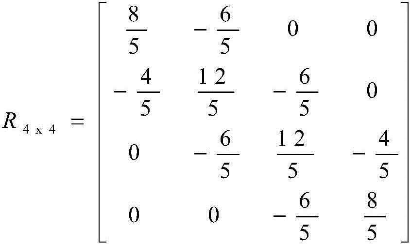
步骤2:将PI调节器中的调节输出送入解耦矩阵R4x4中,输出经解耦矩阵R4x4解耦后,得到第i′个电池组间的输出补偿ωi′;Step 2: send the adjusted output of the PI regulator into the decoupling matrix R 4x4 , and after the output is decoupled by the decoupling matrix R 4x4 , the output compensation ω i' between the i'th battery pack is obtained;
所述解耦矩阵R4x4如下公式所示:The decoupling matrix R 4x4 is shown in the following formula:

步骤3:根据各电池组间的输出补偿ωi′更新各变流器的调制参数,得到各变流器的占空比控制变流器中开关状态,进而调控各电池组的荷电状态,具体方法为:Step 3: Update the modulation parameters of each converter according to the output compensation ω i' between each battery group, obtain the duty ratio of each converter to control the switch state in the converter, and then regulate the state of charge of each battery group, The specific method is:
步骤3.1:根据修正系数λ对变流器的调制系数m进行修正,得到修正后的调制系数m *;Step 3.1: modify the modulation coefficient m of the converter according to the modification coefficient λ to obtain the modified modulation coefficient m * ;
步骤3.1.1:根据各电池组电压计算各电池组间的电压偏置参数yi′,如下公式所示:Step 3.1.1: Calculate the voltage bias parameter y i′ between each battery group according to the voltage of each battery group, as shown in the following formula:

其中,Vi′是第i′个电池组的两端电压;Wherein, Vi ' is the voltage across the i'th battery pack;
步骤3.1.2:根据各电池组间的电压偏置参数计算修正系数λ,如下公式所示:Step 3.1.2: Calculate the correction coefficient λ according to the voltage bias parameters between the battery packs, as shown in the following formula:

步骤3.1.3:令各电池组输出电压均一致,对修正系数λ进行简化,如下公式所示:Step 3.1.3: Make the output voltage of each battery pack consistent, and simplify the correction coefficient λ, as shown in the following formula:

步骤3.1.4:利用简化后的修正系数λ乘以调制系数m,得到修正后的调制系数m*,如下公式所示:Step 3.1.4: Use the simplified correction coefficient λ to multiply the modulation coefficient m to obtain the modified modulation coefficient m * , as shown in the following formula:

步骤3.2:根据修正后的调制系数m*与变流器输出a相电压电角度θ,计算求得每个变流器上IGBT的占空比dxy,其中,1≤x≤3,1≤y≤10;Step 3.2: Calculate the duty cycle d xy of the IGBT on each converter according to the modified modulation coefficient m * and the voltage electrical angle θ of the output a-phase of the converter, where 1≤x≤3, 1≤ y≤10;
步骤3.2.1:将关于输出a相电压电角度θ的正弦函数与变流器的调制系数m*相乘得到第一变流器的占空比d1,然后对正弦函数移相得到第二变流器和第三变流器的占空比d2,d3,如下公式所示:Step 3.2.1: Multiply the sine function of the electrical angle θ of the output a-phase voltage by the modulation coefficient m * of the converter to obtain the duty cycle d 1 of the first converter, and then phase-shift the sine function to obtain the second The duty cycles d 2 , d 3 of the converter and the third converter are as follows:

步骤3.2.2:取三个变流器占空比的最大值Max(dx),将该最大值与各变流器占空比的差值乘以系数k1得到相应变流器上各第一IGBT的占空比dx1(θ),如下公式所示:Step 3.2.2: Take the maximum value Max(d x ) of the duty ratios of the three converters, and multiply the difference between the maximum value and the duty cycle of each converter by the coefficient k 1 to obtain the The duty cycle d x1 (θ) of the first IGBT is given by the following formula:
dx1(θ)=k1*Max[d1(θ),d2(θ),d3(θ)]-dx(θ)d x1 (θ)=k 1 *Max[d 1 (θ), d 2 (θ), d 3 (θ)]-d x (θ)
其中,k1=1/2;Wherein, k 1 =1/2;
步骤3.2.3:取三个变流器占空比的最小值Min(dx),将该最小值与各变流器占空比的差值乘以系数k2得到相应变流器上各第十IGBT的占空比dx,10(θ);Step 3.2.3: Take the minimum value Min(d x ) of the duty ratios of the three converters, and multiply the difference between the minimum value and the duty cycle of each converter by the coefficient k 2 to obtain the The duty cycle d x of the tenth IGBT, 10 (θ);
dx,10(θ)=dx(θ)-k2*Min[d1(θ),d2(θ),d3(θ)]d x, 10 (θ)=d x (θ)-k 2 *Min[d 1 (θ), d 2 (θ), d 3 (θ)]
其中,k2=1/2;Wherein, k 2 =1/2;
步骤3.2.4:计算各变流器上第二至第九IGBT的占空比,如下公式所示:Step 3.2.4: Calculate the duty cycle of the second to ninth IGBTs on each converter, as shown in the following formula:
dx2(θ)=dx3(θ)=…=dx9(θ)=k3(1-dx1(θ)-dx10(θ))d x2 (θ)=d x3 (θ)=…=d x9 (θ)=k 3 (1-d x1 (θ)-d x10 (θ))
其中,k3=1/4;Wherein, k 3 =1/4;
步骤3.3:根据各电池组间的输出补偿ωi′对各变流器的占空比dxy进行补偿,得到补偿后的占空比dxy *,具体方法为:Step 3.3: Compensate the duty cycle d xy of each converter according to the output compensation ω i′ between the battery packs to obtain the compensated duty cycle d xy * , the specific method is as follows:
步骤3.3.1:根据各电池组间的输出补偿计算补偿系数ρ1,将3个变流器中的第一IGBT的占空比dx1(θ)均乘以补偿系数ρ1得到补偿后占空比dx1 *(θ),其中:Step 3.3.1: Calculate the compensation coefficient ρ 1 according to the output compensation between the battery packs, multiply the duty cycle d x1 (θ) of the first IGBT in the three converters by the compensation coefficient ρ 1 to obtain the
ρ1=1-ω2-ω3-ω4-ω5 ρ 1 =1-ω 2 -ω 3 -ω 4 -ω 5
步骤3.3.2:根据各电池组间的输出补偿计算补偿系数ρ2,将3个变流器中的第十IGBT的占空比dx,10(θ)乘以补偿系数ρ2得到补偿后占空比dx,10 *(θ),其中:Step 3.3.2: Calculate the compensation coefficient ρ 2 according to the output compensation between the battery packs, and multiply the duty cycle d x,10 (θ) of the tenth IGBT in the three converters by the compensation coefficient ρ 2 to obtain the compensation Duty cycle d x, 10 * (θ), where:
ρ2=1+ω2+ω3+ω4+ω5 ρ 2 =1+ω 2 +ω 3 +ω 4 +ω 5
步骤3.3.3:将各电池组间的输出补偿ωi′乘以dx1(θ)与dx10(θ)的差值,并将该乘积结果加至dxp(θ),得到各变流器上第二至第九IGBT补偿后占空比dxp *(θ),其中2≤p≤9;Step 3.3.3: Multiply the output compensation ω i′ between the battery packs by the difference between d x1 (θ) and d x10 (θ), and add the multiplication result to d xp (θ) to obtain each converter The duty cycle d xp * (θ) after the compensation of the second to ninth IGBTs on the device, where 2≤p≤9;
步骤3.4利用各变流器的各IGBT补偿后占空比对各电池组的储能进行调控,使各电池组的荷电状态调控至一致。In step 3.4, the post-compensation duty ratio of each IGBT of each converter is used to regulate and control the energy storage of each battery group, so that the state of charge of each battery group is regulated to be consistent.
采用上述技术方案所产生的有益效果在于:本发明提供的一种储能型多电平变流器拓扑及电池荷电状态调控方法,使用该拓扑结构,在变流器6种开关状态下,变流器输出电流都有多种流通路径,这减小了开关管的电压应力,降低了单个开关管的最大能量损耗,提高了储能运行的可靠性。同时针对该拓扑结构提出的电池荷电状态调控方法,根据电池组荷电状态不平衡量,计算电池组间的输出补偿值,进而能够调整变流器的占空比,达到平衡电池组荷电状态的目的,这是一种通过分配各电池组之间的能量流动来平衡各电池组的荷电状态的方法,没有增加额外的能量损耗,大幅度地节省了储能电站的经济成本。The beneficial effects of adopting the above technical solutions are as follows: a topology of an energy storage type multilevel converter and a method for regulating the state of charge of a battery provided by the present invention, using the topology structure, under the six switching states of the converter, The output current of the converter has various flow paths, which reduces the voltage stress of the switch tube, reduces the maximum energy loss of a single switch tube, and improves the reliability of energy storage operation. At the same time, the battery state of charge control method proposed for this topology structure calculates the output compensation value between the battery packs according to the unbalanced state of charge of the battery pack, and then adjusts the duty cycle of the converter to achieve a balanced battery pack state of charge. This is a method to balance the state of charge of each battery group by distributing the energy flow between each battery group, without adding additional energy loss, and greatly saving the economic cost of the energy storage power station.
附图说明Description of drawings
图1为本发明实施例提供的一种储能型多电平变流器拓扑结构示意图;1 is a schematic diagram of a topology structure of an energy storage type multilevel converter according to an embodiment of the present invention;
图2为本发明实施例提供的多电平变流器的拓扑结构图;2 is a topological structure diagram of a multilevel converter provided by an embodiment of the present invention;
图3为本发明实施例提供的多电平变流器处于开关状态1时的开关管状态图;3 is a state diagram of a switch tube when the multilevel converter provided by an embodiment of the present invention is in
图4为本发明实施例提供的多电平变流器处于开关状态2时的开关管状态图;FIG. 4 is a state diagram of a switch tube when the multilevel converter provided by an embodiment of the present invention is in
图5为本发明实施例提供的多电平变流器处于开关状态3时的开关管状态图;FIG. 5 is a state diagram of a switch tube when the multilevel converter provided by an embodiment of the present invention is in
图6为本发明实施例提供的多电平变流器处于开关状态4时的开关管状态图;FIG. 6 is a state diagram of a switch tube when the multilevel converter provided by an embodiment of the present invention is in switch state 4;
图7为本发明实施例提供的多电平变流器处于开关状态5时的开关管状态图;FIG. 7 is a state diagram of a switch tube when the multilevel converter provided by an embodiment of the present invention is in
图8为本发明实施例提供的多电平变流器处于开关状态6时的开关管状态图;FIG. 8 is a state diagram of a switch tube when the multilevel converter provided by an embodiment of the present invention is in
图9为本发明实施例提供的一种储能型多电平变流器拓扑中电池荷电状态调控方法的流程图;9 is a flowchart of a method for regulating the state of charge of a battery in an energy storage type multilevel converter topology according to an embodiment of the present invention;
图10为本发明实施例提供的变流器的各IGBT补偿后占空比仿真图;FIG. 10 is a simulation diagram of the duty cycle after compensation of each IGBT of the converter provided by the embodiment of the present invention;
图11为本发明实施例提供的储能型多电平变流器拓扑中电池荷电状态调控结果的仿真图。FIG. 11 is a simulation diagram of a battery state-of-charge regulation result in an energy-storage-type multilevel converter topology provided by an embodiment of the present invention.
具体实施方式Detailed ways
下面结合附图和实施例,对本发明的具体实施方式作进一步详细描述。以下实施例用于说明本发明,但不用来限制本发明的范围。The specific embodiments of the present invention will be described in further detail below with reference to the accompanying drawings and embodiments. The following examples are intended to illustrate the present invention, but not to limit the scope of the present invention.
本实施例中,一种储能型多电平变流器拓扑,如图1所示,包括5个电池组、5个电容和3个变流器;所述5个电池组分别为电池组一、电池组二、电池组三、电池组四和电池组五,5个电池组串联组成电池组串;5个电池组均由m*n个单体储能电池串并联而成。所述5个电容分别为第一电容器、第二电容器、第三电容器、第四电容器和第五电容器,5个电容串联连接组成电容串;电池组串与电容串并联,每个电池组的正负极与对应的电容正负极相连;所述3个变流器分别为第一变流器、第二变流器和第三变流器,每个变流器均包括50个IGBT管及与其反并联的二极管,如图2所示,所述3个变流器与电池组串正负极并联连接。In this embodiment, an energy storage type multilevel converter topology, as shown in FIG. 1 , includes 5 battery packs, 5 capacitors and 3 converters; the 5 battery packs are battery packs respectively 1.
所述每个变流器中50个IGBT管及与其反并联二极管排列成10x5的矩阵分布,并遵从从左至右,从上至下的顺序,将该50个IGBT及与其反并联二极管标记为Sij,其中1≤i≤10,1≤j≤5,每一列的10个IGBT串联连接,即同一列中上一个IGBT的发射极(E)与下一个IGBT的集电极(C)相连,S31的集电极与第一电容器的下端口相连,S51的集电极与第二电容器的下端口相连,S71的集电极与第三电容器的下端口相连,S91的集电极与第四电容器的下端口相连,S10,1的发射极与第五电容器的下端口相连;S11、S12、S13、S14、S15的集电极并联后与第一电容器的上端口及电池组一的正极连接,S11、S12、S13、S14、S15的发射极相连,S22、S23、S24、S25的发射极相连,S31的发射极与S32的发射极相连,S33、S34、S35的发射极相连,S42的发射极与S43的发射极相连,S44的发射极与S45的发射极相连,S51的发射极与S52的发射极相连,S53的发射极与S54的发射极相连,S62的发射极与S63的发射极相连,S64的发射极与S65的发射极相连,S71的发射极与S72的发射极相连,S73、S74、S75的发射极相连,S82、S83、S84、S85的发射极相连,S91、S92、S93、S94、S95的发射极相连,S10,1、S10,2、S10,3、S10,4、S10,5的发射极并联后与电池组五的负极连接。The 50 IGBT tubes and their anti-parallel diodes in each converter are arranged in a 10x5 matrix distribution, and follow the order from left to right and top to bottom, and the 50 IGBTs and their anti-parallel diodes are marked as S ij , where 1≤i≤10, 1≤j≤5, 10 IGBTs in each column are connected in series, that is, the emitter (E) of the previous IGBT in the same column is connected to the collector (C) of the next IGBT, The collector of S31 is connected to the lower port of the first capacitor, the collector of S51 is connected to the lower port of the second capacitor, the collector of S71 is connected to the lower port of the third capacitor , the collector of S91 is connected to the lower port of the fourth capacitor The lower ports of the capacitors are connected, the emitters of S 10 and 1 are connected to the lower ports of the fifth capacitor; the collectors of S 11 , S 12 , S 13 , S 14 and S 15 are connected in parallel with the upper ports of the first capacitor and the battery The positive poles of group 1 are connected, the emitters of S11 , S12 , S13 , S14 , and S15 are connected, the emitters of S22 , S23 , S24 , and S25 are connected, and the emitter of S31 is connected to the emitter of S32 . The emitter is connected, the emitter of S33 , S34, S35 is connected, the emitter of S42 is connected with the emitter of S43 , the emitter of S44 is connected with the emitter of S45 , the emitter of S51 is connected with S The emitter of 52 is connected to the emitter of S 53 , the emitter of S 53 is connected to the emitter of S 54 , the emitter of S 62 is connected to the emitter of S 63 , the emitter of S 64 is connected to the emitter of S 65 , the emitter of S 71 is connected to the emitter of S 65 Connected to the emitter of S72, connected to the emitter of S73 , S74 , S75 , connected to the emitter of S82 , S83 , S84 , S85 , S91 , S92 , S93 , S94 , S The emitters of 95 are connected to each other, and the emitters of S 10,1 , S 10,2 , S 10,3 , S 10,4 , and S 10,5 are connected in parallel with the negative electrode of the fifth battery pack.
所述每个变流器的IGBT门极(g)根据相应的调制策略有6种不同的开关状态,分别为:The IGBT gate (g) of each converter has 6 different switching states according to the corresponding modulation strategy, which are:
开关状态1:如图3所示,S65、S74、S75、S83、S84、S85、S92、S93、S94、S95、S10,1、S10,2、S10,3、S10,4、S10,5号IGBT导通,变流器的输出电流ip沿着S65、S74、S75、S83、S84、S85、S92、S93、S94、S95、S10,1、S10,2、S10,3、S10,4、S10,5号IGBT形成的任意导通路径流动,S21、S32、S41、S43、S52、S54、S61、S63、S72、S81号IGBT导通用以形成阻断电压,其余IGBT关断,此时变流器的输出电压为0;Switch state 1: As shown in Figure 3, S65 , S74 , S75 , S83 , S84 , S85 , S92 , S93 , S94 , S95 , S10,1 , S10,2 , S 10,3 ,
开关状态2:如图4所示,S54、S55、S63、S64、S65、S72、S73、S74、S75、S81、S82、S83、S84、S85、S91、S92、S93、S94、S95号IGBT导通,变流器的输出电流ip沿着S54、S55、S63、S64、S65、S72、S73、S74、S75、S81、S82、S83、S84、S85、S91、S92、S93、S94、S95号IGBT形成的任意导通路径流动,S21、S32、S41、S43、S52、S54、S61号IGBT导通用以形成阻断电压,其余IGBT关断,此时变流器的输出电压为Vdc/5,其中,Vdc为电池组串两端电压;Switch state 2: As shown in Figure 4, S 54 , S 55 , S 63 , S 64 , S 65 , S 72 , S 73 , S 74 , S 75 , S 81 , S 82 , S 83 , S 84 , S 85 , S 91 , S 92 , S 93 , S 94 , S 95 IGBTs are turned on, and the output current i p of the converter follows S 54 , S 55 , S 63 , S 64 , S 65 , S 72 , S 73 , S74 , S75 , S81 , S82 , S83 , S84 , S85 , S91 , S92 , S93 , S94 , S95 IGBTs form an arbitrary conduction path, S21 , S 32 , S 41 , S 43 , S 52 , S 54 , S 61 IGBTs are turned on to form a blocking voltage, and other IGBTs are turned off. At this time, the output voltage of the converter is V dc /5, where V dc is the voltage across the battery string;
开关状态3:如图5所示,S43、S44、S45、S52、S53、S54、S55、S61、S62、S63、S64、S65、S71、S72、S73、S74、S75、S82、S83、S84、S85号IGBT导通,变流器的输出电流ip沿着S43、S44、S45、S52、S53、S54、S55、S61、S62、S63、S64、S65、S71、S72、S73、S74、S75、S82、S83、S84、S85号IGBT形成的任意导通路径流动,S21、S32、S41、S91号IGBT导通用以形成阻断电压,其余IGBT关断,此时变流器的输出电压为2Vdc/5;Switch state 3: As shown in Figure 5, S 43 , S 44 , S 45 , S 52 , S 53 , S 54 , S 55 , S 61 , S 62 , S 63 , S 64 , S 65 , S 71 , S No. 72 , S73 , S74, S75 , S82 , S83 , S84 , S85 IGBTs are turned on, and the output current i p of the converter follows the steps of S43 , S44 , S45 , S52 , S 53 , S54 , S55 , S61 , S62 , S63 , S64 , S65 , S71 , S72 , S73 , S74 , S75 , S82 , S83 , S84 , S85 Any conduction path formed by the IGBT flows, the IGBTs S 21 , S 32 , S 41 , and S 91 are turned on to form the blocking voltage, and the other IGBTs are turned off. At this time, the output voltage of the converter is 2V dc /5;
开关状态4:如图6所示,S32、S33、S34、S35、S41、S42、S43、S44、S45、S51、S52、S53、S54、S55、S62、S63、S64、S65、S73、S74、S75号IGBT导通,变流器的输出电流ip沿着S32、S33、S34、S35、S41、S42、S43、S44、S45、S51、S52、S53、S54、S55、S62、S63、S64、S65、S73、S74、S75号IGBT形成的任意导通路径流动,S21、S71、S82、S91号IGBT导通用以形成阻断电压,其余IGBT关断,此时变流器的输出电压为3Vdc/5;Switch state 4: As shown in Figure 6, S 32 , S 33 , S 34 , S 35 , S 41 , S 42 , S 43 , S 44 , S 45 , S 51 , S 52 , S 53 , S 54 , S 55 , S 62 , S 63 , S 64 , S 65 , S 73 , S 74 , S 75 IGBTs are turned on, and the output current i p of the converter follows S 32 , S 33 , S 34 , S 35 , S 41 , S42 , S43 , S44 , S45 , S51 , S52 , S53 , S54 , S55 , S62 , S63 , S64 , S65 , S73 , S74 , S75 Any conduction path formed by the IGBT flows, the IGBTs S 21 , S 71 , S 82 and S 91 are turned on to form the blocking voltage, and the other IGBTs are turned off. At this time, the output voltage of the converter is 3V dc /5;
开关状态5:如图7所示,S21、S22、S23、S24、S25、S31、S32、S33、S34、S35、S42、S43、S44、S45、S53、S54、S55、S64、S65号IGBT导通,变流器的输出电流ip沿着S21、S22、S23、S24、S25、S31、S32、S33、S34、S35、S42、S43、S44、S45、S53、S54、S55、S64、S65号IGBT形成的任意导通路径流动,S51、S62、S71、S73、S82、S91号IGBT导通用以形成阻断电压,其余IGBT关断,此时变流器的输出电压为4Vdc/5;Switch state 5: As shown in Figure 7, S 21 , S 22 , S 23 , S 24 , S 25 , S 31 , S 32 , S 33 , S 34 , S 35 , S 42 , S 43 , S 44 , S 45 , S 53 , S 54 , S 55 , S 64 , S 65 IGBTs are turned on, and the output current i p of the converter follows S 21 , S 22 , S 23 , S 24 , S 25 , S 31 , S 32 , S 33 , S 34 , S 35 , S 42 , S 43 , S 44 , S 45 , S 53 , S 54 , S 55 , S 64 , S 65 IGBTs form an arbitrary conduction path to flow, S 51 , IGBTs S 62 , S 71 , S 73 , S 82 and S 91 are turned on to form a blocking voltage, and the other IGBTs are turned off. At this time, the output voltage of the converter is 4V dc /5;
开关状态6:如图8所示,S11、S12、S13、S14、S15、S22、S23、S24、S25、S33、S34、S35、S44、S45、S55号IGBT导通,变流器的输出电流ip沿着S21、S22、S23、S24、S25、S31、S32、S33、S34、S35、S42、S43、S44、S45、S53、S54、S55、S64、S65号IGBT形成的任意导通路径流动,S31、S42、S51、S53、S62、S64、S71、S73、S82、S91号IGBT导通用以形成阻断电压,其余IGBT关断,此时变流器的输出电压为Vdc。Switch state 6: As shown in Figure 8, S 11 , S 12 , S 13 , S 14 , S 15 , S 22 , S 23 , S 24 , S 25 , S 33 , S 34 , S 35 , S 44 , S 45 , S 55 IGBT is turned on, and the output current i p of the converter follows S 21 , S 22 , S 23 , S 24 , S 25 , S 31 , S 32 , S 33 , S 34 , S 35 , S 42 , S 43 , S 44 , S 45 , S 53 , S 54 , S 55 , S 64 , and S 65 IGBTs form an arbitrary conduction path to flow, S 31 , S 42 , S 51 , S 53 , S 62 , IGBTs S 64 , S 71 , S 73 , S 82 , and S 91 are turned on to form a blocking voltage, and the other IGBTs are turned off. At this time, the output voltage of the converter is V dc .
一种储能型多电平变流器拓扑中电池荷电状态的调控方法,如图9所示,具体方法为:A method for regulating the state of charge of a battery in an energy storage multilevel converter topology is shown in Figure 9. The specific method is as follows:
步骤1:计算电池组串中各电池组间的荷电状态不平衡量Imbsoci′,并将其与参考值
步骤1.1:计算电池组串的输出功率P,如下公式所示:Step 1.1: Calculate the output power P of the battery string, as shown in the following formula:

其中,m为变流器的调制系数,Irms是3个变流器输出电流的有效值,Φ是参照相电压的相移角;Among them, m is the modulation coefficient of the converter, I rms is the effective value of the output currents of the three converters, and Φ is the phase shift angle of the reference phase voltage;
根据电池组串的输出功率P求得电池组串的共同电流icom,如下公式所示:The common current i com of the battery strings is obtained according to the output power P of the battery strings, as shown in the following formula:

步骤1.2:根据流经各电池组电流,计算直流调控电流Ii′,Ii′是第i′-1个电池组与第i′个电池组连接点与电容之间的电流,在计算调控电流I2时,令调控电流I3=I4=I5=0,同理在计算其他调控电流时,设置相应的调控电流值为零,则:Step 1.2: Calculate the DC regulation current I i' according to the current flowing through each battery pack, where I i' is the current between the connection point of the i'-1th battery pack and the i'th battery pack and the capacitor. When the current I 2 is used, let the regulation current I 3 =I 4 =I 5 =0. Similarly, when calculating other regulation currents, set the corresponding regulation current value to zero, then:

其中,iBatk是流经第k个电池组的电流,k=1,2,…,5;Among them, i Batk is the current flowing through the kth battery pack, k=1, 2,..., 5;
步骤1.3:根据各电池组荷电状态与直流调控电流计算各电池组间荷电状态不平衡量的计算值Imbsoci′与参考值
步骤1.3.1:根据各电池组荷电状态SoCk计算各电池组间荷电状态不平衡量的计算值Imbsoci′,如下公式所示:Step 1.3.1: According to the state of charge SoC k of each battery pack, calculate the calculated value Imb soci' of the state of charge imbalance between the battery packs, as shown in the following formula:

步骤1.3.2:根据直流调控电流计算各电池组间荷电状态不平衡量的参考值

其中,s拉普拉斯积分算子,Qnom为各电池组的标称容量;Among them, s Laplace integral operator, Q nom is the nominal capacity of each battery pack;
步骤1.4:将差值
步骤2:将PI调节器中的调节输出送入解耦矩阵R4x4中,输出经解耦矩阵R4x4解耦后,得到第i′个电池组间的输出补偿ωi′;Step 2: send the adjusted output of the PI regulator into the decoupling matrix R 4x4 , and after the output is decoupled by the decoupling matrix R 4x4 , the output compensation ω i' between the i'th battery pack is obtained;
所述解耦矩阵R4x4如下公式所示:The decoupling matrix R 4x4 is shown in the following formula:
步骤3:根据各电池组间的输出补偿ωi′更新各变流器的调制参数,得到各变流器的占空比控制变流器中开关状态,进而调控各电池组的荷电状态,具体方法为:Step 3: Update the modulation parameters of each converter according to the output compensation ω i' between each battery group, obtain the duty ratio of each converter to control the switch state in the converter, and then regulate the state of charge of each battery group, The specific method is:
步骤3.1:根据修正系数λ对变流器的调制系数m进行修正,得到修正后的调制系数m*;Step 3.1: modify the modulation coefficient m of the converter according to the modification coefficient λ to obtain the modified modulation coefficient m * ;
步骤3.1.1:根据各电池组电压计算各电池组间的电压偏置参数yi′,如下公式所示:Step 3.1.1: Calculate the voltage bias parameter y i′ between each battery group according to the voltage of each battery group, as shown in the following formula:

其中,Vi′是第i′个电池组的两端电压;Wherein, Vi ' is the voltage across the i'th battery pack;
步骤3.1.2:根据各电池组间的电压偏置参数计算修正系数λ,如下公式所示:Step 3.1.2: Calculate the correction coefficient λ according to the voltage bias parameters between the battery packs, as shown in the following formula:

步骤3.1.3:令各电池组输出电压均一致,对修正系数λ进行简化,如下公式所示:Step 3.1.3: Make the output voltage of each battery pack consistent, and simplify the correction coefficient λ, as shown in the following formula:

步骤3.1.4:利用简化后的修正系数λ乘以调制系数m,得到修正后的调制系数m*,如下公式所示:Step 3.1.4: Use the simplified correction coefficient λ to multiply the modulation coefficient m to obtain the modified modulation coefficient m * , as shown in the following formula:

步骤3.2:根据修正后的调制系数m*与变流器输出a相电压电角度θ,计算求得每个变流器上IGBT的占空比dxy,其中,1≤x≤3,1≤y≤10;Step 3.2: Calculate the duty cycle d xy of the IGBT on each converter according to the modified modulation coefficient m * and the voltage electrical angle θ of the output a-phase of the converter, where 1≤x≤3, 1≤ y≤10;
步骤3.2.1:将关于输出a相电压电角度θ的正弦函数与变流器的调制系数m*相乘得到第一变流器的占空比d1,然后对正弦函数移相得到第二变流器和第三变流器的占空比d2,d3,如下公式所示:Step 3.2.1: Multiply the sine function of the electrical angle θ of the output a-phase voltage by the modulation coefficient m * of the converter to obtain the duty cycle d 1 of the first converter, and then phase-shift the sine function to obtain the second The duty cycles d 2 , d 3 of the converter and the third converter are as follows:

步骤3.2.2:取三个变流器占空比的最大值Max(dx),将该最大值与各变流器占空比的差值乘以系数k1得到相应变流器上各第一IGBT的占空比dx1(θ),如下公式所示:Step 3.2.2: Take the maximum value Max(d x ) of the duty ratios of the three converters, and multiply the difference between the maximum value and the duty cycle of each converter by the coefficient k 1 to obtain the The duty cycle d x1 (θ) of the first IGBT is given by the following formula:
dx1(θ)=k1*Max[d1(θ),d2(θ),d3(θ)]-dx(θ)d x1 (θ)=k 1 *Max[d 1 (θ), d 2 (θ), d 3 (θ)]-d x (θ)
其中,k1=1/2;Wherein, k 1 =1/2;
步骤3.2.3:取三个变流器占空比的最小值Min(dx),将该最小值与各变流器占空比的差值乘以系数k2得到相应变流器上各第十IGBT的占空比dx,10(θ);Step 3.2.3: Take the minimum value Min(d x ) of the duty ratios of the three converters, and multiply the difference between the minimum value and the duty cycle of each converter by the coefficient k 2 to obtain the The duty cycle d x of the tenth IGBT, 10 (θ);
dx,10(θ)=dx(θ)-k2*Min[d1(θ),d2(θ),d3(θ)]d x, 10 (θ)=d x (θ)-k 2 *Min[d 1 (θ), d 2 (θ), d 3 (θ)]
其中,k2=1/2;Wherein, k 2 =1/2;
步骤3.2.4:计算各变流器上第二至第九IGBT的占空比,如下公式所示:Step 3.2.4: Calculate the duty cycle of the second to ninth IGBTs on each converter, as shown in the following formula:
dx2(θ)=dx3(θ)=…=dx9(θ)=k3(1-dx1(θ)-dx10(θ))d x2 (θ)=d x3 (θ)=…=d x9 (θ)=k 3 (1-d x1 (θ)-d x10 (θ))
其中,k3=1/4;Wherein, k 3 =1/4;
步骤3.3:根据各电池组间的输出补偿ωi′对各变流器的占空比dxy进行补偿,得到补偿后的占空比dxy *,具体方法为:Step 3.3: Compensate the duty cycle d xy of each converter according to the output compensation ω i′ between the battery packs to obtain the compensated duty cycle d xy * , the specific method is as follows:
步骤3.3.1:根据各电池组间的输出补偿计算补偿系数ρ1,将3个变流器中的第一IGBT的占空比dx1(θ)均乘以补偿系数ρ1得到补偿后占空比dx1 *(θ),其中:Step 3.3.1: Calculate the compensation coefficient ρ 1 according to the output compensation between the battery packs, multiply the duty cycle d x1 (θ) of the first IGBT in the three converters by the compensation coefficient ρ 1 to obtain the
ρ1=1-ω2-ω3-ω4-ω5 ρ 1 =1-ω 2 -ω 3 -ω 4 -ω 5
步骤3.3.2:根据各电池组间的输出补偿计算补偿系数ρ2,将3个变流器中的第十IGBT的占空比dx,10(θ)乘以补偿系数ρ2得到补偿后占空比dx10 *(θ),其中:Step 3.3.2: Calculate the compensation coefficient ρ 2 according to the output compensation between the battery packs, and multiply the duty cycle d x,10 (θ) of the tenth IGBT in the three converters by the compensation coefficient ρ 2 to obtain the compensation Duty cycle d x10 * (θ), where:
ρ2=1+ω2+ω3+ω4+ω5 ρ 2 =1+ω 2 +ω 3 +ω 4 +ω 5
步骤3.3.3:将各电池组间的输出补偿ωi′乘以dx1(θ)与dx,10(θ)的差值,并将该乘积结果加至dxp(θ),得到各变流器上第二至第九IGBT补偿后占空比dxp *(θ),其中2≤p≤9;Step 3.3.3: Multiply the output compensation ω i′ between each battery pack by the difference between d x1 (θ) and d x, 10 (θ), and add the multiplication result to d xp (θ) to obtain each Duty cycle d xp * (θ) of the second to ninth IGBTs on the converter after compensation, where 2≤p≤9;
步骤3.4利用各变流器的各IGBT补偿后占空比对各电池组的储能进行调控,使各电池组的荷电状态调控至一致。In step 3.4, the post-compensation duty ratio of each IGBT of each converter is used to regulate and control the energy storage of each battery group, so that the state of charge of each battery group is regulated to be consistent.
本实施例中,变流器的各IGBT补偿后占空比仿真如图10所示,利用各变流器的各IGBT补偿后占空比对各电池组的储能进行调控,使各电池组的荷电状态调控至一致的结果如图11所示。In this embodiment, the simulation of the duty cycle of each IGBT of the converter after compensation is shown in Fig. 10, and the energy storage of each battery group is regulated by using the duty cycle of each IGBT of each converter after compensation, so that each battery group is The state of charge was regulated to a consistent result as shown in Figure 11.
最后应说明的是:以上实施例仅用以说明本发明的技术方案,而非对其限制;尽管参照前述实施例对本发明进行了详细的说明,本领域的普通技术人员应当理解:其依然可以对前述实施例所记载的技术方案进行修改,或者对其中部分或者全部技术特征进行等同替换;而这些修改或者替换,并不使相应技术方案的本质脱离本发明权利要求所限定的范围。Finally, it should be noted that the above embodiments are only used to illustrate the technical solutions of the present invention, but not to limit them; although the present invention has been described in detail with reference to the foregoing embodiments, those of ordinary skill in the art should understand that it can still be The technical solutions described in the foregoing embodiments are modified, or some or all of the technical features thereof are equivalently replaced; and these modifications or replacements do not make the essence of the corresponding technical solutions depart from the scope defined by the claims of the present invention.
Claims (9)


Priority Applications (1)
| Application Number | Priority Date | Filing Date | Title |
|---|---|---|---|
| CN201910542733.0A CN110277927B (en) | 2019-06-21 | 2019-06-21 | Energy storage type multi-level converter topology and battery charge state regulation method |
Applications Claiming Priority (1)
| Application Number | Priority Date | Filing Date | Title |
|---|---|---|---|
| CN201910542733.0A CN110277927B (en) | 2019-06-21 | 2019-06-21 | Energy storage type multi-level converter topology and battery charge state regulation method |
Publications (2)
| Publication Number | Publication Date |
|---|---|
| CN110277927A CN110277927A (en) | 2019-09-24 |
| CN110277927B true CN110277927B (en) | 2020-11-06 |
Family
ID=67961413
Family Applications (1)
| Application Number | Title | Priority Date | Filing Date |
|---|---|---|---|
| CN201910542733.0A Expired - Fee Related CN110277927B (en) | 2019-06-21 | 2019-06-21 | Energy storage type multi-level converter topology and battery charge state regulation method |
Country Status (1)
| Country | Link |
|---|---|
| CN (1) | CN110277927B (en) |
Families Citing this family (1)
| Publication number | Priority date | Publication date | Assignee | Title |
|---|---|---|---|---|
| CN116095936B (en) * | 2023-02-13 | 2025-12-02 | 南京工业大学 | Device and method for maintaining pulse power control at different plasma discharge stages |
Citations (9)
| Publication number | Priority date | Publication date | Assignee | Title |
|---|---|---|---|---|
| CN201061144Y (en) * | 2007-04-20 | 2008-05-14 | 上海输配电股份有限公司 | Dynamic voltage compensator with three single-phase structure |
| JP2009171652A (en) * | 2008-01-11 | 2009-07-30 | Toshiba Mitsubishi-Electric Industrial System Corp | Power converter |
| CN202111633U (en) * | 2011-02-24 | 2012-01-11 | 广州智光电气股份有限公司 | A photovoltaic grid-connected inverter |
| CN102403919A (en) * | 2010-09-07 | 2012-04-04 | 夏普株式会社 | Multilevel inverter |
| CN102594187A (en) * | 2012-02-20 | 2012-07-18 | 阳光电源股份有限公司 | Four-level topological unit and application circuit thereof |
| CN104953589A (en) * | 2015-06-08 | 2015-09-30 | 兰州理工大学 | Combined three-phase microgrid system with serially-connected microsource inverters |
| CN205453532U (en) * | 2015-12-31 | 2016-08-10 | 阳光电源股份有限公司 | Five inverter and application circuit thereof |
| JP2019054564A (en) * | 2017-09-12 | 2019-04-04 | ローム株式会社 | AC / DC converter |
| US10658920B2 (en) * | 2015-11-13 | 2020-05-19 | Marquette University | Fault-tolerant topology for multilevel T-type converters |
Family Cites Families (1)
| Publication number | Priority date | Publication date | Assignee | Title |
|---|---|---|---|---|
| BR112018004887A2 (en) * | 2015-09-13 | 2018-10-09 | Alpha Technologies Inc. | power control systems and methods. |
-
2019
- 2019-06-21 CN CN201910542733.0A patent/CN110277927B/en not_active Expired - Fee Related
Patent Citations (9)
| Publication number | Priority date | Publication date | Assignee | Title |
|---|---|---|---|---|
| CN201061144Y (en) * | 2007-04-20 | 2008-05-14 | 上海输配电股份有限公司 | Dynamic voltage compensator with three single-phase structure |
| JP2009171652A (en) * | 2008-01-11 | 2009-07-30 | Toshiba Mitsubishi-Electric Industrial System Corp | Power converter |
| CN102403919A (en) * | 2010-09-07 | 2012-04-04 | 夏普株式会社 | Multilevel inverter |
| CN202111633U (en) * | 2011-02-24 | 2012-01-11 | 广州智光电气股份有限公司 | A photovoltaic grid-connected inverter |
| CN102594187A (en) * | 2012-02-20 | 2012-07-18 | 阳光电源股份有限公司 | Four-level topological unit and application circuit thereof |
| CN104953589A (en) * | 2015-06-08 | 2015-09-30 | 兰州理工大学 | Combined three-phase microgrid system with serially-connected microsource inverters |
| US10658920B2 (en) * | 2015-11-13 | 2020-05-19 | Marquette University | Fault-tolerant topology for multilevel T-type converters |
| CN205453532U (en) * | 2015-12-31 | 2016-08-10 | 阳光电源股份有限公司 | Five inverter and application circuit thereof |
| JP2019054564A (en) * | 2017-09-12 | 2019-04-04 | ローム株式会社 | AC / DC converter |
Also Published As
| Publication number | Publication date |
|---|---|
| CN110277927A (en) | 2019-09-24 |
Similar Documents
| Publication | Publication Date | Title |
|---|---|---|
| CN110380626B (en) | High-power-density single-phase cascade H-bridge rectifier, control method and control system | |
| CN104917418B (en) | A kind of accumulation energy type MMC current transformers of use battery current independent control | |
| CN106877371B (en) | A kind of control method of the modular multi-level converter with energy-storage function | |
| CN106451544B (en) | A kind of united three level grid-connected system control method of light storage | |
| CN110556852A (en) | Distributed energy storage system and control method based on SOC dynamic balance sub-module retrieval | |
| CN106787707A (en) | Embedded accumulation energy type multimode tandem photovoltaic DC booster converter and application process | |
| CN106374767A (en) | Modular multilevel converter sub-module simulation model of considering secondary loop | |
| CN101409453B (en) | Uninterruption power supply | |
| CN204835971U (en) | Multiport power electronic transformer | |
| CN106899030A (en) | A kind of primary side integrated modular independent control battery energy storage system | |
| CN110518793B (en) | Non-isolated bridge arm alternating type direct current transformer based on Boost principle | |
| CN110048629A (en) | A kind of single input switching capacity multi-electrical level inverter and its modulator approach | |
| CN113794393B (en) | A hybrid MMC device loss optimization method based on module decoupling control | |
| CN106877726A (en) | A control method for energy storage converter topology with fault ride-through capability | |
| CN110277927B (en) | Energy storage type multi-level converter topology and battery charge state regulation method | |
| CN109861569A (en) | A Novel Modular Multilevel Converter and Control Method for Suppressing Capacitor Voltage Fluctuation | |
| CN206164198U (en) | Lithium cell power conversion unit | |
| CN205160403U (en) | Energy storage power converting system based on many level of modularization converter | |
| CN113258776B (en) | High-step-up-ratio direct-current converter for large-scale offshore wind power direct current output | |
| CN118157091A (en) | A joint control method for DC power spring topology based on cascaded half-bridge | |
| CN111030494A (en) | Neutral point potential balance control method for T-type three-level topology converter | |
| CN118889611A (en) | A battery cluster series-parallel balanced energy storage system and control method thereof | |
| CN116131338A (en) | Direct-current power spring topology and control method based on cascaded half bridge | |
| CN118367779A (en) | Gain adjustable hybrid DC transformer and voltage conversion and control method and system | |
| Mounica et al. | Battery management for integrating renewable energy systems to the DC Micro-grid |
Legal Events
| Date | Code | Title | Description |
|---|---|---|---|
| PB01 | Publication | ||
| PB01 | Publication | ||
| SE01 | Entry into force of request for substantive examination | ||
| SE01 | Entry into force of request for substantive examination | ||
| GR01 | Patent grant | ||
| GR01 | Patent grant | ||
| CF01 | Termination of patent right due to non-payment of annual fee | ||
| CF01 | Termination of patent right due to non-payment of annual fee |
Granted publication date: 20201106 |