CN110220881B - Flexible SERS substrate based on nanostructure and ordered nanoparticles and preparation method and application thereof - Google Patents

Flexible SERS substrate based on nanostructure and ordered nanoparticles and preparation method and application thereof Download PDF

Info

Publication number
CN110220881B
CN110220881B CN201910380665.2A CN201910380665A CN110220881B CN 110220881 B CN110220881 B CN 110220881B CN 201910380665 A CN201910380665 A CN 201910380665A CN 110220881 B CN110220881 B CN 110220881B
Authority
CN
China
Prior art keywords
resin layer
grooves
light
cured resin
nano
Prior art date
Legal status (The legal status is an assumption and is not a legal conclusion. Google has not performed a legal analysis and makes no representation as to the accuracy of the status listed.)
Active
Application number
CN201910380665.2A
Other languages
Chinese (zh)
Other versions
CN110220881A (en
Inventor
张成鹏
姜兆亮
刘文平
马嵩华
Current Assignee (The listed assignees may be inaccurate. Google has not performed a legal analysis and makes no representation or warranty as to the accuracy of the list.)
Shandong University
Original Assignee
Shandong University
Priority date (The priority date is an assumption and is not a legal conclusion. Google has not performed a legal analysis and makes no representation as to the accuracy of the date listed.)
Filing date
Publication date
Application filed by Shandong University filed Critical Shandong University
Priority to CN201910380665.2A priority Critical patent/CN110220881B/en
Publication of CN110220881A publication Critical patent/CN110220881A/en
Priority to LU101707A priority patent/LU101707B1/en
Application granted granted Critical
Publication of CN110220881B publication Critical patent/CN110220881B/en
Active legal-status Critical Current
Anticipated expiration legal-status Critical

Links

Images

Classifications

    • BPERFORMING OPERATIONS; TRANSPORTING
    • B05SPRAYING OR ATOMISING IN GENERAL; APPLYING FLUENT MATERIALS TO SURFACES, IN GENERAL
    • B05DPROCESSES FOR APPLYING FLUENT MATERIALS TO SURFACES, IN GENERAL
    • B05D3/00Pretreatment of surfaces to which liquids or other fluent materials are to be applied; After-treatment of applied coatings, e.g. intermediate treating of an applied coating preparatory to subsequent applications of liquids or other fluent materials
    • B05D3/12Pretreatment of surfaces to which liquids or other fluent materials are to be applied; After-treatment of applied coatings, e.g. intermediate treating of an applied coating preparatory to subsequent applications of liquids or other fluent materials by mechanical means
    • BPERFORMING OPERATIONS; TRANSPORTING
    • B81MICROSTRUCTURAL TECHNOLOGY
    • B81BMICROSTRUCTURAL DEVICES OR SYSTEMS, e.g. MICROMECHANICAL DEVICES
    • B81B7/00Microstructural systems; Auxiliary parts of microstructural devices or systems
    • B81B7/04Networks or arrays of similar microstructural devices
    • BPERFORMING OPERATIONS; TRANSPORTING
    • B81MICROSTRUCTURAL TECHNOLOGY
    • B81CPROCESSES OR APPARATUS SPECIALLY ADAPTED FOR THE MANUFACTURE OR TREATMENT OF MICROSTRUCTURAL DEVICES OR SYSTEMS
    • B81C1/00Manufacture or treatment of devices or systems in or on a substrate
    • B81C1/00015Manufacture or treatment of devices or systems in or on a substrate for manufacturing microsystems
    • B81C1/00023Manufacture or treatment of devices or systems in or on a substrate for manufacturing microsystems without movable or flexible elements
    • B81C1/00031Regular or irregular arrays of nanoscale structures, e.g. etch mask layer
    • BPERFORMING OPERATIONS; TRANSPORTING
    • B81MICROSTRUCTURAL TECHNOLOGY
    • B81CPROCESSES OR APPARATUS SPECIALLY ADAPTED FOR THE MANUFACTURE OR TREATMENT OF MICROSTRUCTURAL DEVICES OR SYSTEMS
    • B81C1/00Manufacture or treatment of devices or systems in or on a substrate
    • B81C1/00349Creating layers of material on a substrate
    • B81C1/00373Selective deposition, e.g. printing or microcontact printing
    • CCHEMISTRY; METALLURGY
    • C23COATING METALLIC MATERIAL; COATING MATERIAL WITH METALLIC MATERIAL; CHEMICAL SURFACE TREATMENT; DIFFUSION TREATMENT OF METALLIC MATERIAL; COATING BY VACUUM EVAPORATION, BY SPUTTERING, BY ION IMPLANTATION OR BY CHEMICAL VAPOUR DEPOSITION, IN GENERAL; INHIBITING CORROSION OF METALLIC MATERIAL OR INCRUSTATION IN GENERAL
    • C23CCOATING METALLIC MATERIAL; COATING MATERIAL WITH METALLIC MATERIAL; SURFACE TREATMENT OF METALLIC MATERIAL BY DIFFUSION INTO THE SURFACE, BY CHEMICAL CONVERSION OR SUBSTITUTION; COATING BY VACUUM EVAPORATION, BY SPUTTERING, BY ION IMPLANTATION OR BY CHEMICAL VAPOUR DEPOSITION, IN GENERAL
    • C23C14/00Coating by vacuum evaporation, by sputtering or by ion implantation of the coating forming material
    • C23C14/06Coating by vacuum evaporation, by sputtering or by ion implantation of the coating forming material characterised by the coating material
    • C23C14/14Metallic material, boron or silicon
    • C23C14/20Metallic material, boron or silicon on organic substrates
    • CCHEMISTRY; METALLURGY
    • C23COATING METALLIC MATERIAL; COATING MATERIAL WITH METALLIC MATERIAL; CHEMICAL SURFACE TREATMENT; DIFFUSION TREATMENT OF METALLIC MATERIAL; COATING BY VACUUM EVAPORATION, BY SPUTTERING, BY ION IMPLANTATION OR BY CHEMICAL VAPOUR DEPOSITION, IN GENERAL; INHIBITING CORROSION OF METALLIC MATERIAL OR INCRUSTATION IN GENERAL
    • C23CCOATING METALLIC MATERIAL; COATING MATERIAL WITH METALLIC MATERIAL; SURFACE TREATMENT OF METALLIC MATERIAL BY DIFFUSION INTO THE SURFACE, BY CHEMICAL CONVERSION OR SUBSTITUTION; COATING BY VACUUM EVAPORATION, BY SPUTTERING, BY ION IMPLANTATION OR BY CHEMICAL VAPOUR DEPOSITION, IN GENERAL
    • C23C14/00Coating by vacuum evaporation, by sputtering or by ion implantation of the coating forming material
    • C23C14/22Coating by vacuum evaporation, by sputtering or by ion implantation of the coating forming material characterised by the process of coating
    • C23C14/24Vacuum evaporation
    • GPHYSICS
    • G01MEASURING; TESTING
    • G01NINVESTIGATING OR ANALYSING MATERIALS BY DETERMINING THEIR CHEMICAL OR PHYSICAL PROPERTIES
    • G01N21/00Investigating or analysing materials by the use of optical means, i.e. using sub-millimetre waves, infrared, visible or ultraviolet light
    • G01N21/62Systems in which the material investigated is excited whereby it emits light or causes a change in wavelength of the incident light
    • G01N21/63Systems in which the material investigated is excited whereby it emits light or causes a change in wavelength of the incident light optically excited
    • G01N21/65Raman scattering
    • G01N21/658Raman scattering enhancement Raman, e.g. surface plasmons
    • BPERFORMING OPERATIONS; TRANSPORTING
    • B05SPRAYING OR ATOMISING IN GENERAL; APPLYING FLUENT MATERIALS TO SURFACES, IN GENERAL
    • B05DPROCESSES FOR APPLYING FLUENT MATERIALS TO SURFACES, IN GENERAL
    • B05D1/00Processes for applying liquids or other fluent materials
    • B05D1/40Distributing applied liquids or other fluent materials by members moving relatively to surface
    • BPERFORMING OPERATIONS; TRANSPORTING
    • B05SPRAYING OR ATOMISING IN GENERAL; APPLYING FLUENT MATERIALS TO SURFACES, IN GENERAL
    • B05DPROCESSES FOR APPLYING FLUENT MATERIALS TO SURFACES, IN GENERAL
    • B05D2201/00Polymeric substrate or laminate
    • B05D2201/02Polymeric substrate
    • BPERFORMING OPERATIONS; TRANSPORTING
    • B05SPRAYING OR ATOMISING IN GENERAL; APPLYING FLUENT MATERIALS TO SURFACES, IN GENERAL
    • B05DPROCESSES FOR APPLYING FLUENT MATERIALS TO SURFACES, IN GENERAL
    • B05D2252/00Sheets
    • B05D2252/02Sheets of indefinite length
    • BPERFORMING OPERATIONS; TRANSPORTING
    • B05SPRAYING OR ATOMISING IN GENERAL; APPLYING FLUENT MATERIALS TO SURFACES, IN GENERAL
    • B05DPROCESSES FOR APPLYING FLUENT MATERIALS TO SURFACES, IN GENERAL
    • B05D3/00Pretreatment of surfaces to which liquids or other fluent materials are to be applied; After-treatment of applied coatings, e.g. intermediate treating of an applied coating preparatory to subsequent applications of liquids or other fluent materials
    • B05D3/06Pretreatment of surfaces to which liquids or other fluent materials are to be applied; After-treatment of applied coatings, e.g. intermediate treating of an applied coating preparatory to subsequent applications of liquids or other fluent materials by exposure to radiation
    • B05D3/061Pretreatment of surfaces to which liquids or other fluent materials are to be applied; After-treatment of applied coatings, e.g. intermediate treating of an applied coating preparatory to subsequent applications of liquids or other fluent materials by exposure to radiation using U.V.
    • B05D3/065After-treatment
    • B05D3/067Curing or cross-linking the coating
    • BPERFORMING OPERATIONS; TRANSPORTING
    • B05SPRAYING OR ATOMISING IN GENERAL; APPLYING FLUENT MATERIALS TO SURFACES, IN GENERAL
    • B05DPROCESSES FOR APPLYING FLUENT MATERIALS TO SURFACES, IN GENERAL
    • B05D5/00Processes for applying liquids or other fluent materials to surfaces to obtain special surface effects, finishes or structures
    • B05D5/02Processes for applying liquids or other fluent materials to surfaces to obtain special surface effects, finishes or structures to obtain a matt or rough surface
    • BPERFORMING OPERATIONS; TRANSPORTING
    • B05SPRAYING OR ATOMISING IN GENERAL; APPLYING FLUENT MATERIALS TO SURFACES, IN GENERAL
    • B05DPROCESSES FOR APPLYING FLUENT MATERIALS TO SURFACES, IN GENERAL
    • B05D7/00Processes, other than flocking, specially adapted for applying liquids or other fluent materials to particular surfaces or for applying particular liquids or other fluent materials
    • B05D7/02Processes, other than flocking, specially adapted for applying liquids or other fluent materials to particular surfaces or for applying particular liquids or other fluent materials to macromolecular substances, e.g. rubber
    • B05D7/04Processes, other than flocking, specially adapted for applying liquids or other fluent materials to particular surfaces or for applying particular liquids or other fluent materials to macromolecular substances, e.g. rubber to surfaces of films or sheets
    • BPERFORMING OPERATIONS; TRANSPORTING
    • B05SPRAYING OR ATOMISING IN GENERAL; APPLYING FLUENT MATERIALS TO SURFACES, IN GENERAL
    • B05DPROCESSES FOR APPLYING FLUENT MATERIALS TO SURFACES, IN GENERAL
    • B05D7/00Processes, other than flocking, specially adapted for applying liquids or other fluent materials to particular surfaces or for applying particular liquids or other fluent materials
    • B05D7/50Multilayers
    • B05D7/52Two layers
    • B05D7/54No clear coat specified
    • B05D7/546No clear coat specified each layer being cured, at least partially, separately
    • BPERFORMING OPERATIONS; TRANSPORTING
    • B81MICROSTRUCTURAL TECHNOLOGY
    • B81BMICROSTRUCTURAL DEVICES OR SYSTEMS, e.g. MICROMECHANICAL DEVICES
    • B81B2203/00Basic microelectromechanical structures
    • B81B2203/03Static structures
    • B81B2203/0353Holes
    • BPERFORMING OPERATIONS; TRANSPORTING
    • B81MICROSTRUCTURAL TECHNOLOGY
    • B81BMICROSTRUCTURAL DEVICES OR SYSTEMS, e.g. MICROMECHANICAL DEVICES
    • B81B2207/00Microstructural systems or auxiliary parts thereof
    • B81B2207/05Arrays
    • B81B2207/056Arrays of static structures
    • GPHYSICS
    • G01MEASURING; TESTING
    • G01NINVESTIGATING OR ANALYSING MATERIALS BY DETERMINING THEIR CHEMICAL OR PHYSICAL PROPERTIES
    • G01N21/00Investigating or analysing materials by the use of optical means, i.e. using sub-millimetre waves, infrared, visible or ultraviolet light
    • G01N21/62Systems in which the material investigated is excited whereby it emits light or causes a change in wavelength of the incident light
    • G01N21/63Systems in which the material investigated is excited whereby it emits light or causes a change in wavelength of the incident light optically excited
    • G01N21/65Raman scattering
    • G01N2021/653Coherent methods [CARS]
    • G01N2021/655Stimulated Raman

Landscapes

  • Chemical & Material Sciences (AREA)
  • Engineering & Computer Science (AREA)
  • Health & Medical Sciences (AREA)
  • Analytical Chemistry (AREA)
  • General Health & Medical Sciences (AREA)
  • Immunology (AREA)
  • Nuclear Medicine, Radiotherapy & Molecular Imaging (AREA)
  • Physics & Mathematics (AREA)
  • Life Sciences & Earth Sciences (AREA)
  • Manufacturing & Machinery (AREA)
  • Mechanical Engineering (AREA)
  • Biochemistry (AREA)
  • Microelectronics & Electronic Packaging (AREA)
  • Pathology (AREA)
  • General Physics & Mathematics (AREA)
  • Chemical Kinetics & Catalysis (AREA)
  • Materials Engineering (AREA)
  • Metallurgy (AREA)
  • Organic Chemistry (AREA)
  • Computer Hardware Design (AREA)
  • Nanotechnology (AREA)
  • Investigating, Analyzing Materials By Fluorescence Or Luminescence (AREA)

Abstract

本发明属于柔性电子薄膜技术领域,尤其涉及基于纳米结构和有序纳米颗粒的柔性SERS基底及其制备方法和应用。所述SERS基底包括:柔性薄膜基材、光固化树脂层、凹槽、金属薄膜层和纳米颗粒,其中:所述光固化树脂层设置在柔性薄膜基材的表面上,所述凹槽呈阵列式分布在光固化树脂层上且与光固化树脂层一体化成型,所述金属薄膜层覆盖在光固化树脂层和凹槽表面,所述纳米颗粒有序填充在凹槽之中。本发明将光固化树脂层和凹槽进行了金属化,并通过纳米结构和有序纳米颗粒的协同作用实现拉曼信号增强,具有精度高、灵敏度高、稳定性好、信号重现性强等优点。

Figure 201910380665

The invention belongs to the technical field of flexible electronic films, and in particular relates to a flexible SERS substrate based on nanostructures and ordered nanoparticles and a preparation method and application thereof. The SERS substrate includes: a flexible film substrate, a photocurable resin layer, grooves, a metal film layer and nanoparticles, wherein: the photocurable resin layer is arranged on the surface of the flexible film substrate, and the grooves are in an array The metal film layer is distributed on the photocurable resin layer and integrally formed with the photocurable resin layer, the metal film layer covers the photocurable resin layer and the surface of the groove, and the nanoparticles are filled in the groove in an orderly manner. The invention metallizes the photocurable resin layer and the groove, and realizes Raman signal enhancement through the synergistic effect of nanostructure and ordered nanoparticle, and has the advantages of high precision, high sensitivity, good stability, strong signal reproducibility, etc. advantage.

Figure 201910380665

Description

Flexible SERS substrate based on nanostructure and ordered nanoparticles and preparation method and application thereof
Technical Field
The invention belongs to the technical field of flexible electronic thin films, and particularly relates to a flexible SERS substrate based on a nano structure and ordered nanoparticles, and a preparation method and application thereof.
Background
This information disclosed in this background of the invention is only for the purpose of increasing an understanding of the general background of the invention and is not necessarily to be taken as an acknowledgement or any form of suggestion that this information forms the prior art already known to a person skilled in the art.
The Surface Enhanced Raman Scattering (SERS) can amplify molecular signals adsorbed on the metal surface by 1015 times, even can realize single molecule detection, is a high-sensitivity spectroscopic technology, and is widely applied to the fields of material science, surface science, analytical chemistry, biology, diagnostics and the like.
The surface-enhanced raman spectroscopy test requires that signals have stability and reproducibility, mainly depends on the nanometer structure of the surface-enhanced substrate and the orderliness and uniformity of nanoparticles, and the rapid preparation of the SERS substrate with high precision, high sensitivity, good stability and strong signal reproducibility becomes a problem to be solved urgently.
Patent document CN 109187487 a discloses a surface-enhanced raman scattering substrate of silver nanoclusters, and a preparation method and application thereof, wherein the patent discloses that the raman signal enhancement is realized by preparing nano silver particle clusters through an electrochemical displacement reaction. However, the inventors believe that: the patent document only realizes the SERS function through the nano silver particles, and the nano silver particles are randomly distributed, so that the signal reproducibility of repeated detection cannot be ensured.
Patent document CN 109239051 a discloses a flexible transferable SERS substrate, which is obtained by modifying thiolated polystyrene onto noble metal nanoparticles through ligand exchange, and then assembling the thiolated polystyrene into an ordered two-dimensional noble metal nano superlattice film without a substrate and self-supporting on a porous substrate through a gas-liquid interface self-assembly method. However, the inventors believe that: the patent document has the defects of complex manufacturing process, low efficiency, high cost and the like, and only can realize two-dimensional assembly of single-layer metal particles through a self-assembly process, so that ordered arrangement of multiple layers of metal particles cannot be realized, and the Raman signal enhancement effect is weakened.
Disclosure of Invention
In view of the problems in the prior art, the present invention aims to provide a flexible SERS substrate based on nanostructures and ordered nanoparticles, and a preparation method and application thereof. The method provided by the invention is low in cost, high in efficiency and suitable for large-scale batch processing, and the prepared SERS substrate can realize high-precision, high-sensitivity, stability and reproducibility test of Raman signals.
The invention provides a flexible SERS substrate based on a nano structure and ordered nano particles.
The invention also provides a preparation method of the flexible SERS substrate based on the nano structure and the ordered nano particles.
The invention also provides a flexible SERS substrate based on the nano structure and the ordered nano particles and an application of the preparation method.
In order to realize the purpose, the invention discloses the following technical scheme:
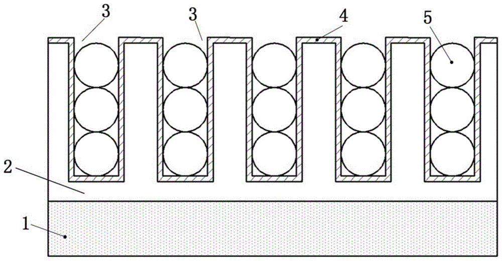
first, the present invention discloses a flexible SERS substrate based on nanostructures and ordered nanoparticles, comprising: flexible film substrate, photocuring resin layer, recess, metal thin film layer and nanoparticle, wherein: the light-cured resin layer is arranged on the surface of the flexible film substrate, the grooves are distributed on the light-cured resin layer in an array mode, the grooves and the light-cured resin layer are integrally formed, the metal film layer covers the light-cured resin layer and the surfaces of the grooves, and the nano particles are orderly filled in the grooves.
As a further technical solution, the flexible film substrate includes: polyethylene terephthalate (PET), Polycarbonate (PC), polypropylene (PP), polyvinyl chloride (PVC), polymethyl methacrylate (PMMA), and the like.
As a further technical solution, the metal thin film layer and the nanoparticles are made of materials with raman signal enhancement function, such as: gold, silver, copper, platinum, and the like.
As a further technical solution, the shape of the groove includes: any one or more of a cylindrical structure, a rectangular parallelepiped structure, a square structure, a prismatic structure, and the like.
As a further technical solution, the array shape formed by the grooves includes: rectangular arrays, square arrays, hexagonal arrays, circular arrays, diamond arrays, triangular arrays, or the like.
As a further technical scheme, the thickness of the metal film layer is 3nm-100 nm.
As a further technical scheme, the diameter of the nano-particles is 1nm-200 nm.
As a further technical scheme, the diameter or the side length of the groove is larger than the diameter of the nano-particles and smaller than 1.4 times of the diameter of the nano-particles; the diameter of the groove is slightly larger than that of the nano particles, so that the nano particles can be smoothly filled; however, the diameter of the groove is not too large, so that each layer in the longitudinal direction can only contain one nano particle, the position of the nano particles can be limited to the maximum extent, and the order of the nano particles in the longitudinal direction is ensured.
As a further technical scheme, the depth of the groove is 1.5nm-500 nm.
As a further technical scheme, the distance between the grooves is 5nm-1000 nm.
Secondly, the invention discloses a preparation method of the flexible SERS substrate based on the nano structure and the ordered nano particles, which comprises the following steps:
(1) coating a light-cured resin material on the surface of a flexible film substrate to form a light-cured resin layer, and impressing the light-cured resin layer through a roll-to-roll ultraviolet curing process to obtain grooves integrally formed with the light-cured resin layer, wherein the grooves are distributed on the light-cured resin layer in an array manner;
(2) depositing a metal film layer on the light-cured resin layer and the surface of the groove by adopting an evaporation coating technology to metalize the metal film layer so as to have an SERS function;
(3) and filling the nano particles in the grooves to ensure that the nano particles are orderly distributed in the grooves, thus obtaining the nano-particle material.
As a further technical scheme, in the roll-to-roll ultraviolet curing process, the imprinting speed is 0.5-60m/min, and the extrusion force is 1-9kg/cm2The temperature of the mould is 10-100 ℃.
As a further technical scheme, in the evaporation coating process, the vacuum degree is 1 multiplied by 10-5-4×10⁻⁵Pa。
As a further technical scheme, the filling of the nanoparticles adopts a blade coating process, and can be selected as follows: blade-coating the nano-particle solution in gaps among the grooves, and wiping off the redundant nano-particle solution on the surface by using alcohol; optionally, the speed of the blade coating is 0.1-100 mm/s.
Finally, the invention discloses the use of the flexible SERS substrate based on nanostructures and ordered nanoparticles in electronic devices; and the application of the preparation method of the flexible SERS substrate in preparing flexible electronic materials.
Compared with the prior art, the invention has the following beneficial effects:
(1) the method provided by the invention is low in cost, high in efficiency and suitable for large-scale batch processing, and the prepared SERS substrate can realize high-precision, high-sensitivity, stability and reproducibility test of Raman signals.
(2) The invention metallizes the light-cured resin layer and the groove, so that the structure array has triple functions: the metalized grooves can generate hot spots to excite plasma resonance, so that the function of enhancing the Raman signal intensity is realized; in addition, the groove can limit the nano particles, so that the nano particles can keep order and consistency in a large area, and the stability and reproducibility test of Raman signals can be realized; moreover, on the basis of the 'hot spots' generated between the grooves, a great number of 'hot spots' can be generated between the metalized grooves and the nanoparticles, and the detection accuracy and sensitivity of the Raman signal are further improved.
(3) The array structure formed by the grooves regulates the uniformity and the order of the nano particles, realizes Raman signal enhancement through the synergistic effect of the nano structure and the ordered nano particles, and has the advantages of high precision, high sensitivity, good stability, strong signal reproducibility and the like.
Drawings
The accompanying drawings, which are incorporated in and constitute a part of this specification, are included to provide a further understanding of the invention, and are incorporated in and constitute a part of this specification, illustrate exemplary embodiments of the invention and together with the description serve to explain the invention and not to limit the invention.
Fig. 1 is a cross-sectional view of a flexible SERS substrate based on nanostructures and ordered nanoparticles according to example 1 of the present invention.
Fig. 2 is a top view of a flexible SERS substrate based on nanostructures and ordered nanoparticles according to example 1 of the present invention.
Fig. 3 is a process flow diagram of the preparation of the flexible SERS substrate based on nanostructures and ordered nanoparticles in example 2 of the present invention.
The reference numerals in the drawings denote: 1-flexible film substrate, 2-photocuring resin layer, 3-groove, 4-metal film layer and 5-nano particle.
Detailed Description
It should be noted that the following detailed description is exemplary and is intended to provide further explanation of the disclosure. Unless defined otherwise, all technical and scientific terms used herein have the same meaning as commonly understood by one of ordinary skill in the art to which this application belongs.
It is noted that the terminology used herein is for the purpose of describing particular embodiments only and is not intended to be limiting of example embodiments according to the present application. As used herein, the singular forms "a", "an" and "the" are intended to include the plural forms as well, and it should be understood that when the terms "comprises" and/or "comprising" are used in this specification, they specify the presence of stated features, steps, operations, devices, components, and/or combinations thereof, unless the context clearly indicates otherwise.
As described in the background art, the surface enhanced raman spectroscopy requires a signal with stability and reproducibility, mainly depends on the nanostructure of the surface enhanced substrate and the order and uniformity of the nanoparticles, and the rapid preparation of the SERS substrate with high precision, high sensitivity, good stability and strong signal reproducibility is a problem to be solved. Therefore, the invention provides a flexible SERS substrate based on a nano structure and ordered nano particles and a preparation method thereof; the invention will now be further described with reference to the accompanying drawings and detailed description.
Example 1
A flexible SERS substrate based on nanostructures and ordered nanoparticles, with reference to fig. 1 and 2, comprising: flexible film substrate 1, photocuring resin layer 2, recess 3, metal thin film layer 4 and nanoparticle 5, wherein: the light-cured resin layer 2 is arranged on the surface of the flexible film substrate 1, the grooves 3 are of a cylindrical structure, are distributed on the light-cured resin layer 2 in a square array and are integrally formed with the light-cured resin layer 2, the metal film layer 4 covers the surfaces of the light-cured resin layer 2 and the grooves 3, and the nano particles 5 are orderly filled in the grooves 3; the flexible film base material 1 is made of polyethylene terephthalate (PET); the metal film layer 4 and the nano particles 5 are nano silver particles; the thickness of the metal film layer 4 is 15 nm; the diameter of the nanoparticles 5 is 20 nm; the depth of the groove 3 is 100nm, and the diameter of the groove is 25 nm; the spacing between the grooves 3 is 60 nm.
Example 2
A flexible SERS substrate based on nanostructures and ordered nanoparticles, as in example 1, with the following differences: the grooves 3 are of a cuboid structure and are distributed on the light-cured resin layer 2 in a rectangular array; the material of the flexible film substrate 1 is Polycarbonate (PC); the thickness of the metal film layer 4 is 30 nm; the metal film layer 4 and the nano particles 5 are all nano gold particles; the diameter of the nanoparticle is 10 nm; the depth of the groove 3 is 20nm, and the diameter of the groove is 10.5 nm; the distance between the grooves 3 is 10 nm.
Example 3
A flexible SERS substrate based on nanostructures and ordered nanoparticles, as in example 1, with the following differences: the grooves 3 are of a cubic structure and distributed on the light-cured resin layer 2 in a hexagonal array; the flexible film substrate 1 is made of polyvinyl chloride (PVC); the thickness of the metal film layer 4 is 50 nm; the metal film layer 4 and the nano particles 5 are both nano copper particles; the diameter of the nanoparticle is 15 nm; the depth of the groove 3 is 20nm, and the diameter of the groove is 15.5 nm; the spacing between the grooves 3 is 60 nm.
Example 4
A flexible SERS substrate based on nanostructures and ordered nanoparticles, as in example 1, with the following differences: the grooves 3 are of prismatic structures and are distributed on the light-cured resin layer 2 in a circular array; the flexible film substrate 1 is made of polymethyl methacrylate (PMMA); the thickness of the metal film layer 4 is 60 nm; the metal film layer 4 and the nano particles 5 are nano silver particles; the diameter of the nanoparticle is 50 nm; the depth of the groove 3 is 150nm, and the diameter of the groove is 70 nm; the spacing between the grooves 3 is 150 nm.
Example 5
A flexible SERS substrate based on nanostructures and ordered nanoparticles, as in example 1, with the following differences: the flexible film base material 1 is made of polypropylene (PP); the thickness of the metal film layer 4 is 3 nm; the metal film layer 4 and the nano particles 5 are both nano platinum particles; the diameter of the nanoparticle is 1 nm; the depth of the groove 3 is 1.5nm, and the diameter of the groove is 1.4 nm; the spacing between the grooves 3 is 5 nm.
Example 6
A flexible SERS substrate based on nanostructures and ordered nanoparticles, as in example 2, with the following differences: the grooves 3 are distributed on the light-cured resin layer 2 in a rhombic array; the thickness of the metal film layer is 100 nm; the diameter of the nanoparticle is 80 nm; the depth of the groove 3 is 200nm, and the diameter of the groove is 100 nm; the spacing between the grooves 3 is 200 nm.
Example 7
A flexible SERS substrate based on nanostructures and ordered nanoparticles, as in example 3, with the following differences: the grooves are distributed on the light-cured resin layer 2 in a triangular array; the thickness of the metal film layer 4 is 20 nm; the diameter of the nanoparticle is 200 nm; the depth of the groove 3 is 300nm, and the diameter of the groove is 250 nm; the spacing between the grooves 3 is 500 nm.
Example 8
A flexible SERS substrate based on nanostructures and ordered nanoparticles, as in example 5, with the following differences: the thickness of the metal film layer 4 is 50 nm; the diameter of the nanoparticle is 120 nm; the depth of the groove 3 is 500nm, and the diameter of the groove is 150 nm; the spacing between the grooves 3 is 1000 nm.
Example 9
A flexible SERS substrate based on nanostructures and ordered nanoparticles, as in example 1, with the following differences: the thickness of the metal film layer 4 is 25 nm; the diameter of the nanoparticle is 45 nm; the depth of the groove 3 is 300nm, and the diameter of the groove is 50 nm; the spacing between the grooves 3 is 600 nm.
Example 10
A flexible SERS substrate based on nanostructures and ordered nanoparticles, as in example 1, with the following differences: the light-curing resin layer 2, the groove 3, and the metal thin-film layer 4 are not provided.
Example 11
A flexible SERS substrate based on nanostructures and ordered nanoparticles, as in example 1, with the following differences: there are no nanoparticles.
Example 12
A flexible SERS substrate based on nanostructures and ordered nanoparticles, as in example 1, with the following differences: there is no photocurable resin layer 2, grooves 3, metal thin-film layer 4, and nanoparticles 5, i.e., only flexible thin-film substrate 1.
Example 13
The method for preparing the flexible SERS substrate based on nanostructures and ordered nanoparticles according to example 1 includes the following steps:
(1) coating a light-cured resin material on the surface of a flexible film substrate to form a light-cured resin layer, and impressing the light-cured resin layer through a roll-to-roll ultraviolet curing process to obtain grooves integrally formed with the light-cured resin layer, wherein the grooves are distributed on the light-cured resin layer in an array manner; in the roll-to-roll ultraviolet curing process, the imprinting speed is 20m/min, and the extrusion force is 5kg/cm2The temperature of the die is 50 ℃;
(2) depositing a metal film layer on the surface of the light-cured resin layer and the groove by an evaporation coating technology, wherein in the evaporation coating technology, the vacuum degree is 3.5 multiplied by 10-5Pa;
(3) Blade-coating the nanoparticle solution in gaps among the grooves 3, and wiping off the redundant nanoparticle solution on the surface by using alcohol to ensure that the nanoparticles are orderly distributed among the grooves to obtain the nano-particle cleaning agent; the draw-down speed was 20 mm/s.
Statistical table of signal enhancement factor, relative standard deviation of multi-point tests for flexible SERS substrates prepared in examples 1-12. During detection, a rhodamine 6G solution is used as a marker, the laser wavelength is 785nm, the power is 1mW, the integration time is 10s, and the Raman signal enhancement factor at the 1366-1 peak is calculated. The calculation of the relative standard deviation is to randomly select 9 positions from the surface of the sample for raman signal characterization, and calculate the relative standard deviation of the raman signal enhancement factors measured at different positions, and the result is shown in table 1.
TABLE 1
Figure BDA0002053273070000091
The above description is only a preferred embodiment of the present application and is not intended to limit the present application, and various modifications and changes may be made by those skilled in the art. Any modification, equivalent replacement, improvement and the like made within the spirit and principle of the present application shall be included in the protection scope of the present application.

Claims (2)

1. A flexible SERS substrate based on nanostructures and ordered nanoparticles, comprising: flexible film substrate, photocuring resin layer, recess, metal thin film layer and nanoparticle, wherein: the light-cured resin layer is arranged on the surface of the flexible film substrate, the grooves are of a cylindrical structure, are distributed on the light-cured resin layer in a square array and are integrally formed with the light-cured resin layer, the metal film layer covers the light-cured resin layer and the surfaces of the grooves, and the nano particles are orderly filled in the grooves; the flexible film base material is polyethylene terephthalate; the metal film layer and the nano particles are nano silver particles; the thickness of the metal film layer is 15 nm; the diameter of the nanoparticle is 20 nm; the depth of the groove is 100nm, and the diameter of the groove is 25 nm; the distance between the grooves is 60 nm;
the preparation method of the flexible SERS substrate based on the nano structure and the ordered nanoparticles comprises the following steps:
(1) coating a light-cured resin material on the surface of a flexible film substrate to form a light-cured resin layer, and impressing the light-cured resin layer through a roll-to-roll ultraviolet curing process to obtain grooves integrally formed with the light-cured resin layer, wherein the grooves are distributed on the light-cured resin layer in an array manner; in the roll-to-roll ultraviolet curing process, the imprinting speed is 20m/min, and the extrusion force is 5kg/cm2The temperature of the die is 50 ℃;
(2) depositing a metal film layer on the surface of the light-cured resin layer and the groove by an evaporation coating technologyIn the process, the vacuum degree is 3.5 multiplied by 10-5Pa;
(3) Blade-coating the nano-particle solution in gaps among the grooves, and wiping off the redundant nano-particle solution on the surface by using alcohol to ensure that the nano-particles are orderly distributed among the grooves to obtain the nano-particle cleaning agent; the draw-down speed was 20 mm/s.
2. Use of the nanostructure and ordered nanoparticle-based flexible SERS substrate according to claim 1 in an electronic device.
CN201910380665.2A 2019-05-08 2019-05-08 Flexible SERS substrate based on nanostructure and ordered nanoparticles and preparation method and application thereof Active CN110220881B (en)

Priority Applications (2)

Application Number Priority Date Filing Date Title
CN201910380665.2A CN110220881B (en) 2019-05-08 2019-05-08 Flexible SERS substrate based on nanostructure and ordered nanoparticles and preparation method and application thereof
LU101707A LU101707B1 (en) 2019-05-08 2020-03-27 Flexible sers substrate based on nano-structures and ordered nano-particles, and preparation method and application thereof

Applications Claiming Priority (1)

Application Number Priority Date Filing Date Title
CN201910380665.2A CN110220881B (en) 2019-05-08 2019-05-08 Flexible SERS substrate based on nanostructure and ordered nanoparticles and preparation method and application thereof

Publications (2)

Publication Number Publication Date
CN110220881A CN110220881A (en) 2019-09-10
CN110220881B true CN110220881B (en) 2021-03-23

Family

ID=67820588

Family Applications (1)

Application Number Title Priority Date Filing Date
CN201910380665.2A Active CN110220881B (en) 2019-05-08 2019-05-08 Flexible SERS substrate based on nanostructure and ordered nanoparticles and preparation method and application thereof

Country Status (2)

Country Link
CN (1) CN110220881B (en)
LU (1) LU101707B1 (en)

Families Citing this family (10)

* Cited by examiner, † Cited by third party
Publication number Priority date Publication date Assignee Title
CN111272714A (en) * 2020-03-03 2020-06-12 电子科技大学中山学院 Metal oxide gas sensor based on optical resonant cavity principle
CN111951662B (en) * 2020-06-03 2022-06-10 中山大学 A physical information hiding structure based on the size difference of structural units and its preparation method
CN112683879B (en) * 2020-12-22 2023-03-17 山东大学 Polymer-based multielement surface enhanced Raman detection substrate and preparation method thereof
CN113702354A (en) * 2021-09-02 2021-11-26 电子科技大学 Flexible SERS substrate based on array type microstructure and preparation method thereof
CN114280028A (en) * 2021-12-29 2022-04-05 国家纳米科学中心 A medium-enhanced Raman scattering chip and its preparation method and application
CN114295599B (en) * 2021-12-29 2024-09-27 国家纳米科学中心 Surface-enhanced Raman scattering chip and preparation method and application thereof
CN114324293B (en) * 2021-12-29 2024-09-27 国家纳米科学中心 Surface-enhanced Raman chip
CN115078325A (en) * 2022-05-27 2022-09-20 南京邮电大学 Surface-enhanced Raman active microneedle array sensor and preparation method and application thereof
CN115165842A (en) * 2022-07-12 2022-10-11 山东大学 Electrically-controlled flexible SERS substrate based on piezoelectric composite film and preparation method and application thereof
CN117607121B (en) * 2023-11-10 2024-07-30 元珵科技(北京)有限公司 A special slide for Raman spectrum scanning of biological tissue

Family Cites Families (3)

* Cited by examiner, † Cited by third party
Publication number Priority date Publication date Assignee Title
CN103279009B (en) * 2013-06-14 2015-09-30 中国科学院光电技术研究所 Flexible ultraviolet light imprinting composite template and preparation method thereof
CN107290326B (en) * 2016-04-12 2020-07-17 中国科学院苏州纳米技术与纳米仿生研究所 Chip device and manufacturing method thereof
CN109470679B (en) * 2017-09-08 2021-04-23 清华大学 Molecular Carriers for Molecular Detection

Also Published As

Publication number Publication date
CN110220881A (en) 2019-09-10
LU101707B1 (en) 2020-07-27

Similar Documents

Publication Publication Date Title
CN110220881B (en) Flexible SERS substrate based on nanostructure and ordered nanoparticles and preparation method and application thereof
Jambhulkar et al. Nanoparticle assembly: From self‐organization to controlled micropatterning for enhanced functionalities
Suresh et al. Fabrication of large-area flexible SERS substrates by nanoimprint lithography
JP6252053B2 (en) Surface-enhanced Raman scattering measurement substrate and manufacturing method thereof
Liu et al. A high-performance and low cost SERS substrate of plasmonic nanopillars on plastic film fabricated by nanoimprint lithography with AAO template
Abu Hatab et al. Surface-enhanced Raman spectroscopy substrates created via electron beam lithography and nanotransfer printing
Malaquin et al. Controlled particle placement through convective and capillary assembly
Liu et al. Three-dimensional SERS hot spots for chemical sensing: Towards developing a practical analyzer
Cao et al. Optical field enhancement in Au nanoparticle-decorated nanorod arrays prepared by femtosecond laser and their tunable surface-enhanced Raman scattering applications
Barcelo et al. Fabrication of deterministic nanostructure assemblies with sub-nanometer spacing using a nanoimprinting transfer technique
US9513226B2 (en) Nanochip based surface plasmon resonance sensing devices and techniques
Watanabe et al. Spontaneous formation of cluster array of gold particles by convective self-assembly
Sun et al. Three-dimensional colloidal crystal-assisted lithography for two-dimensional patterned arrays
Lipomi et al. Use of thin sectioning (nanoskiving) to fabricate nanostructures for electronic and optical applications
Zhang et al. Fabrication of gold-coated PDMS surfaces with arrayed triangular micro/nanopyramids for use as SERS substrates
Wang et al. Flexible and superhydrophobic silver nanoparticles decorated aligned silver nanowires films as surface-enhanced Raman scattering substrates
Yilmaz et al. High-rate assembly of nanomaterials on insulating surfaces using electro-fluidic directed assembly
Zheng et al. Layer-by-layer assembly of three-dimensional optical functional nanostructures
WO2014120156A1 (en) Surface enhanced fluorescence spectroscopy apparatus
WO2019146692A1 (en) Analysis substrate
CN110314830B (en) Flexible Surface-Enhanced Raman Scattering Substrate Based on Monolayer Ordered Nanoparticle Arrays
Xia et al. DNA transport in hierarchically-structured colloidal-nanoparticle porous-wall nanochannels
Shin et al. Fabrication of 50 nm scale Pt nanostructures by block copolymer (BCP) and its characteristics of surface-enhanced Raman scattering (SERS)
Jang et al. Electromagnetic field enhancement in the multilayer of metallic nanomesh films: synthesis and application as surface-enhanced Raman scattering substrates
Park et al. Fabrication of highly uniform three-dimensional SERS substrates by control of wettability

Legal Events

Date Code Title Description
PB01 Publication
PB01 Publication
SE01 Entry into force of request for substantive examination
GR01 Patent grant
GR01 Patent grant