CN110049261B - Pixel structure, image sensor and terminal - Google Patents
Pixel structure, image sensor and terminal Download PDFInfo
- Publication number
- CN110049261B CN110049261B CN201910329816.1A CN201910329816A CN110049261B CN 110049261 B CN110049261 B CN 110049261B CN 201910329816 A CN201910329816 A CN 201910329816A CN 110049261 B CN110049261 B CN 110049261B
- Authority
- CN
- China
- Prior art keywords
- photodiode
- pixel structure
- light
- size
- type
- Prior art date
- Legal status (The legal status is an assumption and is not a legal conclusion. Google has not performed a legal analysis and makes no representation as to the accuracy of the status listed.)
- Expired - Fee Related
Links
Images


Classifications
-
- H—ELECTRICITY
- H04—ELECTRIC COMMUNICATION TECHNIQUE
- H04N—PICTORIAL COMMUNICATION, e.g. TELEVISION
- H04N25/00—Circuitry of solid-state image sensors [SSIS]; Control thereof
- H04N25/70—SSIS architectures; Circuits associated therewith
-
- H—ELECTRICITY
- H04—ELECTRIC COMMUNICATION TECHNIQUE
- H04N—PICTORIAL COMMUNICATION, e.g. TELEVISION
- H04N25/00—Circuitry of solid-state image sensors [SSIS]; Control thereof
- H04N25/70—SSIS architectures; Circuits associated therewith
- H04N25/71—Charge-coupled device [CCD] sensors; Charge-transfer registers specially adapted for CCD sensors
- H04N25/75—Circuitry for providing, modifying or processing image signals from the pixel array
Landscapes
- Engineering & Computer Science (AREA)
- Multimedia (AREA)
- Signal Processing (AREA)
- Solid State Image Pick-Up Elements (AREA)
Abstract
Description
技术领域technical field
本申请涉及图像技术,尤其涉及一种像素结构、图像传感器及终端。The present application relates to image technology, and in particular, to a pixel structure, an image sensor and a terminal.
背景技术Background technique
互补金属氧化物半导体图像传感器(Complementary Metal OxideSemiconductor Image Sensor,CIS)是一种图形收集处理半导体器件,光电二极管(Photo-Diode,PD)作为光电转换器件应用于CIS中,使得CIS实现将光信号转化成电信号进行存储和显示。Complementary Metal Oxide Semiconductor Image Sensor (CIS) is a kind of semiconductor device for image collection and processing. Photo-Diode (PD) is used in CIS as a photoelectric conversion device, so that CIS can realize the conversion of optical signals. The electrical signal is stored and displayed.
现有的CIS需要基于较大的CIS尺寸去获得较高的像素数,比如,索尼公司的IMX586,其1/2英寸的传感器像素数为4800万,CIS中每英寸的像素数量已经接近极限,若再减小像素尺寸PD的量子效率也会随之降低,影响成像效果。因此,CIS无法满足高像素小尺寸的要求,导致配置有CIS的摄像头模组的整体尺寸偏大。The existing CIS needs to obtain a higher pixel count based on a larger CIS size. For example, Sony's IMX586 has a 1/2-inch sensor with 48 million pixels. The number of pixels per inch in CIS is close to the limit. If the pixel size is further reduced, the quantum efficiency of PD will also decrease, which will affect the imaging effect. Therefore, the CIS cannot meet the requirements of high pixel size and small size, resulting in a larger overall size of the camera module equipped with the CIS.
发明内容SUMMARY OF THE INVENTION
为解决上述技术问题,本申请实施例期望提供一种像素结构、图像传感器及终端,能够使图像传感器满足小尺寸高像素的要求。In order to solve the above technical problems, the embodiments of the present application expect to provide a pixel structure, an image sensor and a terminal, which can make the image sensor meet the requirements of small size and high pixels.
本申请的技术方案是这样实现的:The technical solution of the present application is realized as follows:
第一方面,提供了一种像素结构,其特征在于,所述像素结构包括:至少一个光电二极管和读出电路;In a first aspect, a pixel structure is provided, wherein the pixel structure includes: at least one photodiode and a readout circuit;
所述至少一个光电二极管的感光区域与所述像素结构的进光口相对,用于吸收至少一种特定波长的光信号,将吸收到的光信号转化为电信号;其中,感光区域尺寸不同的光电二极管所能吸收的特定波长的光信号不同;The photosensitive area of the at least one photodiode is opposite to the light inlet of the pixel structure, and is used for absorbing at least one light signal of a specific wavelength, and converting the absorbed light signal into an electrical signal; wherein the photosensitive area has different sizes. Photodiodes can absorb different wavelengths of light signals;
所述读出电路与所述至少一个光电二极管相连,用于读出所述至少一个光电二极管的电信号。The readout circuit is connected to the at least one photodiode for reading out electrical signals of the at least one photodiode.
上述方案中,所述至少一个光电二极管具体用于根据感光区域的共振波长吸收至少一种特定波长的光信号;其中,所述共振波长为所述光电二极管的感光区域发生共振吸收时的波长;不同尺寸的感光区域对应不同的共振波长。In the above solution, the at least one photodiode is specifically used to absorb at least one optical signal of a specific wavelength according to the resonance wavelength of the photosensitive region; wherein, the resonance wavelength is the wavelength at which resonance absorption occurs in the photosensitive region of the photodiode; Photosensitive regions of different sizes correspond to different resonance wavelengths.
上述方案中,所述像素结构包括至少两个光电二极管时,所述至少两个光电二极管用于将至少两种特定波长的光信号转化为电信号。In the above solution, when the pixel structure includes at least two photodiodes, the at least two photodiodes are used to convert optical signals of at least two specific wavelengths into electrical signals.
上述方案中,所述至少一个光电二极管包括:第一类光电二极管、第二类光电二极管和第三类光电二极管;其中,所述第一类光电二极管的感光区域尺寸为第一尺寸,用于吸收第一种特定波长的光信号;所述第二类光电二极管的感光区域尺寸为第二尺寸,用于吸收第二种特定波长的光信号;所述第三类光电二极管的感光区域尺寸为第三尺寸,用于吸收第三种特定波长的光信号。In the above solution, the at least one photodiode includes: a first type of photodiode, a second type of photodiode, and a third type of photodiode; wherein, the size of the photosensitive area of the first type of photodiode is a first size, which is used for Absorbing the optical signal of the first specific wavelength; the photosensitive area of the second type of photodiode has a second size for absorbing the optical signal of the second specific wavelength; the photosensitive area of the third type of photodiode has a size of The third dimension is used to absorb the light signal of the third specific wavelength.
上述方案中,所述第一种特定波长的光信号为蓝光,所述第二种特定波长的光信号为绿光,所述第三种特定波长的光信号为红光时,所述第一尺寸小于所述第二尺寸,所述第二尺寸小于第三尺寸。In the above solution, when the optical signal of the first specific wavelength is blue light, the optical signal of the second specific wavelength is green light, and the optical signal of the third specific wavelength is red light, the first The size is smaller than the second size, and the second size is smaller than the third size.
上述方案中,所述第一类光电二极管的数量、所述第二类光电二极管的数量与所述第三类光电二极管的数量不完全相同。In the above solution, the number of the first type of photodiodes, the number of the second type of photodiodes and the number of the third type of photodiodes are not exactly the same.
上述方案中,所述像素结构包含一个光电二极管时,所述像素还包括滤光片;所述滤光片位于所述光电二极管的感光区域与所述进光口之间,用于对所述进光口的入射光线进行过滤,得到一种能被所述光电二极管吸收的特定波长的光信号;所述感光区域的面积小于所述进光口的横截面积。In the above solution, when the pixel structure includes a photodiode, the pixel further includes a filter; the filter is located between the photosensitive region of the photodiode and the light inlet, and is used to The incident light of the light inlet is filtered to obtain a light signal of a specific wavelength that can be absorbed by the photodiode; the area of the photosensitive region is smaller than the cross-sectional area of the light inlet.
上述方案中,所述光电二极管形状为圆柱;其中,所述光电二极管的感光区域为所述圆柱的其中一个圆形底面。In the above solution, the photodiode is in the shape of a cylinder; wherein, the photosensitive region of the photodiode is one of the circular bottom surfaces of the cylinder.
第二方面,提供了一种图像传感器,所述图像传感器包括上述任一种所述的像素结构。In a second aspect, an image sensor is provided, and the image sensor includes any one of the pixel structures described above.
第三方面,提供了一种终端,所述终端包括上述图像传感器。In a third aspect, a terminal is provided, and the terminal includes the above-mentioned image sensor.
采用上述技术方案,像素结构中包含至少一个光电二极管,通过调整光电二极管的感光区域尺寸,使至少一个光电二极管吸收至少一种特定波长的光信号,且能够保证光电二极管具有较高的量子效率。如此,解决了像素结构尺寸太小导致的光电二极管量子效率过低的问题,满足了图像传感器的小尺寸高像素的要求。With the above technical solution, the pixel structure includes at least one photodiode, and by adjusting the size of the photodiode photosensitive area, the at least one photodiode absorbs at least one light signal of a specific wavelength, and the photodiode can be guaranteed to have high quantum efficiency. In this way, the problem that the quantum efficiency of the photodiode is too low due to the too small pixel structure size is solved, and the requirements of the image sensor for small size and high pixels are satisfied.
附图说明Description of drawings
图1为本申请实施例中像素结构的组成结构示意图1;FIG. 1 is a schematic diagram 1 of a composition structure of a pixel structure in an embodiment of the present application;
图2为本申请实施例中像素结构的第一局部示意图;FIG. 2 is a first partial schematic diagram of a pixel structure in an embodiment of the present application;
图3为本申请实施例中像素结构的第一剖面示意图;3 is a first cross-sectional schematic diagram of a pixel structure in an embodiment of the present application;
图4为本申请实施例中像素结构的第二局部示意图;FIG. 4 is a second partial schematic diagram of a pixel structure in an embodiment of the present application;
图5为本申请实施例中像素结构的第二剖面示意图;5 is a second cross-sectional schematic diagram of a pixel structure in an embodiment of the present application;
图6为本申请实施例中像素结构的第三局部示意图;6 is a third partial schematic diagram of a pixel structure in an embodiment of the present application;
图7为本申请实施例中图像传感器的组成结构示意图;FIG. 7 is a schematic diagram of the composition and structure of an image sensor in an embodiment of the present application;
图8为本申请实施例中终端的组成结构示意图。FIG. 8 is a schematic diagram of the composition and structure of a terminal in an embodiment of the present application.
具体实施方式Detailed ways
为了能够更加详尽地了解本申请实施例的特点与技术内容,下面结合附图对本申请实施例的实现进行详细阐述,所附附图仅供参考说明之用,并非用来限定本申请实施例。In order to have a more detailed understanding of the features and technical contents of the embodiments of the present application, the implementation of the embodiments of the present application will be described in detail below with reference to the accompanying drawings.
实施例一Example 1
在实际应用中,像素结构作为图像传感器的重要组成部分,能够完成对接收到的自然光进行光电转换,从而得到电信号,然而,像素结构的像素尺寸大约为600nm左右时,光电二极管的拥有较高量子效率,像素结构的尺寸减小,使光电二极管的感光区域面积减小从而使光电二极管的量子效率降低,影响图像传感器的成像效果。In practical applications, the pixel structure, as an important part of the image sensor, can complete the photoelectric conversion of the received natural light to obtain an electrical signal. However, when the pixel size of the pixel structure is about 600nm, the photodiode has a higher Quantum efficiency, the size of the pixel structure is reduced, the area of the photosensitive region of the photodiode is reduced, the quantum efficiency of the photodiode is reduced, and the imaging effect of the image sensor is affected.
这里,量子效率是衡量某个颜色通道某个频率/波长的光子转换成电子的效率,传统的像素结构,随着像素尺寸的不断缩减,光电二极管的感光区域面积也随着减小,使得光电二极管的电荷收集势阱中可容纳的最大信号电荷量即满阱容量(简称,阱容量)受到抑制,阱容量受到抑制使得小尺寸像素的动态范围、信噪比和灵敏度等指标恶化,而这些指标都将直接影响小尺寸像素的成像质量。Here, quantum efficiency is a measure of the efficiency of converting photons of a certain frequency/wavelength of a certain color channel into electrons. With the traditional pixel structure, as the pixel size continues to shrink, the photosensitive area of the photodiode also decreases, making the photoelectric The maximum amount of signal charge that can be accommodated in the charge collection potential well of the diode, that is, the full well capacity (referred to as well capacity) is suppressed, and the suppression of the well capacity makes the dynamic range, signal-to-noise ratio and sensitivity of small-sized pixels deteriorate. All indicators will directly affect the imaging quality of small-sized pixels.
为了满足图像传感器的小尺寸高像素的要求,本申请实施例提供了一种图像传感器中的像素结构。如图1所示,像素结构10,包括至少一个光电二极管101和读出电路102;其中,In order to meet the requirements of image sensors with small size and high pixels, embodiments of the present application provide a pixel structure in an image sensor. As shown in FIG. 1, the pixel structure 10 includes at least one photodiode 101 and a readout circuit 102; wherein,
所述至少一个光电二极管101的感光区域与所述像素结构的进光口相对,用于吸收至少一种特定波长的光信号,将吸收到的光信号转化为电信号;其中,感光区域尺寸不同的光电二极管所能吸收的特定波长的光信号不同;The photosensitive region of the at least one photodiode 101 is opposite to the light inlet of the pixel structure, and is used for absorbing at least one light signal of a specific wavelength, and converting the absorbed light signal into an electrical signal; wherein the photosensitive regions have different sizes Different photodiodes can absorb light signals of specific wavelengths;
所述读出电路102与所述至少一个光电二极管101相连,用于读出所述至少一个光电二极管的电信号。The readout circuit 102 is connected to the at least one photodiode 101 for reading out electrical signals of the at least one photodiode.
入射光穿过进光口进入到像素结构内部,被光电二极管101吸收后转化为电信号,读出电路102读出光电二极管的电信号用于颜色感知。The incident light enters the pixel structure through the light inlet, is absorbed by the photodiode 101 and converted into an electrical signal, and the readout circuit 102 reads out the electrical signal of the photodiode for color perception.
其中,所述至少一个光电二极管具体用于根据感光区域的共振波长吸收至少一种特定波长的光信号;其中,所述共振波长为所述光电二极管的感光区域发生共振吸收时的波长;不同尺寸的感光区域对应不同的共振波长。Wherein, the at least one photodiode is specifically used to absorb at least one optical signal of a specific wavelength according to the resonance wavelength of the photosensitive region; wherein, the resonance wavelength is the wavelength at which resonance absorption occurs in the photosensitive region of the photodiode; different sizes The photosensitive regions correspond to different resonant wavelengths.
这里,当像素结构中呈正方形的进光口的边长小于特定波长时,为了防止特定波长被衍射掉,本申请实施例利用光电二极管的感光区域的共振吸收特性,使得光电二极管根据其感光区域的共振波长对特定波长进行吸收。Here, when the side length of the square light inlet in the pixel structure is smaller than the specific wavelength, in order to prevent the specific wavelength from being diffracted, the embodiment of the present application utilizes the resonance absorption characteristics of the photodiode's photosensitive region, so that the photodiode can be based on its photosensitive region. The resonant wavelength of , absorbs a specific wavelength.
实际应用中,光电二极管的感光区域可以为光电二极管的上表面,光电二极管的共振波长与光电二极管的感光区域的折射率和尺寸有关,所以,可以通过调整感光区域的折射率,和/或,感光区域的尺寸,来调整光电二极管的共振波长。In practical applications, the photosensitive region of the photodiode may be the upper surface of the photodiode, and the resonant wavelength of the photodiode is related to the refractive index and size of the photosensitive region of the photodiode. Therefore, by adjusting the refractive index of the photosensitive region, and/or, The size of the photosensitive region to adjust the resonance wavelength of the photodiode.
本申请实施例中,通过调整光电二极管的感光区域尺寸来调整共振波长,以使得特定波长在光电二极管的感光区域的共振波长范围之内,这样,得到的较小尺寸光电二极管能够对特定波长的光信号实现共振吸收,使得其在较小的感光区域下仍然拥有较高的量子效率。In the embodiments of the present application, the resonance wavelength is adjusted by adjusting the size of the photosensitive region of the photodiode, so that the specific wavelength is within the resonance wavelength range of the photosensitive region of the photodiode. The optical signal achieves resonance absorption, so that it still has a high quantum efficiency in a small photosensitive area.
为了减小光电二极管之间的耦合,在一些实施例中,光电二极管为柱体,比如,圆柱、棱柱。柱体的上表面为感光区域,感光区域可以为规则形状或不规则形状,比如,感光区域为正多边形。柱形体感光区域的面积小于进光口的横截面积。To reduce coupling between photodiodes, in some embodiments, the photodiodes are cylinders, eg, cylinders, prisms. The upper surface of the cylinder is a photosensitive area, and the photosensitive area can be of regular shape or irregular shape, for example, the photosensitive area is a regular polygon. The area of the photosensitive region of the cylindrical body is smaller than the cross-sectional area of the light inlet.
可选的,所述光电二极管形状为圆柱;其中,所述光电二极管的感光区域为所述圆柱的其中一个圆形底面。圆形底面的直径小于正方形进光口的边长,比如,正方形进光口的边长为100nm,圆形底面直径为70nm。Optionally, the photodiode is in the shape of a cylinder; wherein, the photosensitive area of the photodiode is one of the circular bottom surfaces of the cylinder. The diameter of the circular bottom surface is smaller than the side length of the square light inlet. For example, the side length of the square light inlet is 100 nm, and the diameter of the circular bottom surface is 70 nm.
可选的,所述光电二极管形状为正四棱柱;其中,所述光电二极管的感光区域为所述正四棱柱的其中一个正方形底面。正方形底面的边长小于正方形进光口的边长,比如,正方形进光口的边长为100nm,圆形底面直径为70nm。Optionally, the photodiode is in the shape of a regular quadrangular prism; wherein, the photosensitive area of the photodiode is one of the square bottom surfaces of the regular quadrangular prism. The side length of the square bottom surface is smaller than the side length of the square light inlet. For example, the side length of the square light inlet is 100 nm, and the diameter of the circular bottom surface is 70 nm.
也就是说,在制作图像传感器时,需要将每个像素结构中的光电二极管与相邻像素结构的光电二极管之间留有间隔,由于光电二极管发生共振吸收时会使得边缘场很强,增加间隔是为了防止相邻像素结构的光电二极管之间光的相互串扰。所以,在工艺上光电二极管采用感光区域面积小于进光口横截面积的柱形结构不仅可以实现对光的共振吸收,还可以更好的控制相邻两个光电二极管的间隔。That is to say, when fabricating an image sensor, it is necessary to leave a space between the photodiodes in each pixel structure and the photodiodes of adjacent pixel structures. Since the photodiode resonance absorption will make the fringe field strong, increasing the space This is to prevent mutual crosstalk of light between photodiodes of adjacent pixel structures. Therefore, in the process, the photodiode adopts a columnar structure with a photosensitive area smaller than the cross-sectional area of the light inlet, which can not only achieve resonance absorption of light, but also better control the interval between two adjacent photodiodes.
实际应用中,在像素结构尺寸小于特定波长时,只需要调整光电二极管的感光区域的尺寸,便可以得到不同的共振波长,使得特定波长的光通过共振吸收的方式被光电二极管吸收,使得其在较小的感光区域下仍然拥有较高的量子效率。In practical applications, when the size of the pixel structure is smaller than a specific wavelength, it is only necessary to adjust the size of the photosensitive region of the photodiode to obtain different resonance wavelengths, so that the light of a specific wavelength is absorbed by the photodiode through resonance absorption, so that it is A smaller photosensitive area still has a higher quantum efficiency.
为了使光电二极管在较小的感光区域下仍然拥有较高的量子效率,在一种可选的实施例中,特定波长在共振波长的范围之内。由于光电二极管的感光区域的共振波长与感光区域的形状有关,不同的形状的感光区域的共振波长可以是一个波长范围,其中,可以是特定波长的一部分位于共振波长的范围之内,也可以是特定波长全部在共振波长的范围之内。In order to make the photodiode still have higher quantum efficiency under a smaller photosensitive area, in an optional embodiment, the specific wavelength is within the range of the resonance wavelength. Since the resonance wavelength of the photosensitive region of the photodiode is related to the shape of the photosensitive region, the resonance wavelength of the photosensitive region of different shapes can be a wavelength range, wherein a part of the specific wavelength can be located within the range of the resonance wavelength, or it can be The specific wavelengths are all within the range of resonance wavelengths.
针对上述特定波长来说,在一种可选的实施例中,特定波长的光包括以下任意一项:红光波长,绿光波长,蓝光波长。For the above specific wavelength, in an optional embodiment, the light of the specific wavelength includes any one of the following: red light wavelength, green light wavelength, and blue light wavelength.
也就是说,像素结构内不同光电二极管分别可以吸收红色、绿色或者蓝色。That is, different photodiodes within the pixel structure can absorb red, green, or blue, respectively.
在一些实施例中,所述像素结构包含一个光电二极管时,所述像素还包括滤光片;所述滤光片位于所述光电二极管的感光区域与所述进光口之间,用于对所述进光口的入射光线进行过滤,得到一种能被所述光电二极管吸收的特定波长的光信号;所述感光区域的面积小于所述进光口的横截面积。In some embodiments, when the pixel structure includes a photodiode, the pixel further includes a filter; the filter is located between the photosensitive area of the photodiode and the light inlet, and is used for The incident light of the light inlet is filtered to obtain a light signal with a specific wavelength that can be absorbed by the photodiode; the area of the photosensitive region is smaller than the cross-sectional area of the light inlet.
实际应用中,上述滤光片可以是用于过滤红光的红色滤光片,也可以是用于过滤绿光的绿色滤光片,还可以是用于过滤蓝光的蓝色滤光片,这里,本申请实施例不作具体限定。In practical applications, the above-mentioned filter can be a red filter for filtering red light, a green filter for filtering green light, or a blue filter for filtering blue light, here , the embodiments of the present application are not specifically limited.
图2中示出了一种图像传感器,图像传感器20在1/3.6英寸的感光面上拥有40000*30000个像素,单个像素21局部放大图为正方形结构,单个像素中包含一个圆柱形PD,每个像素的正方形结构边长为100nm。图像传感器的每个像素中含有1个圆柱形PD,通过圆柱形PD结构的光电二极管的共振吸收特性吸收不同特定波长的光,比如,蓝光对应PD的底面直径为60nm,使得其在较小的感光区域下仍然拥有较高的量子效率。借助于这样的亚波长超小像素结构,可以在1/3.6英寸的单色图像传感器上实现12亿的像素数,展示了一种移动端超高像素的单色图像传感器的方法。适应性的调整圆柱形PD的底面直径,和像素的边框长度,像素能够吸收其他特定波长的光,比如,绿光对应PD底面直径为90nm,红光对应PD底面直径为120nm。Figure 2 shows an image sensor. The
图3中示出了单个像素内部的纵向剖面示意图,像素21包括位于进光口下方的滤光片211,位于滤光片211下方的光电二极管212,以及与光电二极管212负极相连的金属排线213,这里,金属排线即为读出电路,用于读出光电二极管的电信号。FIG. 3 shows a schematic longitudinal cross-sectional view of the interior of a single pixel. The
传统的像素结构一般也是包括滤光片和光电二极管,光电二极管的感光区域与滤光片基本等大同形,然而,针对小尺寸像素结构来说采用传统的光电二极管的结构,量子效率较低,为了使其拥有较高的量子效率,可以通过调整光电二极管的感光区域的共振波长的方式,这里,主要是通过缩小光电二极管的感光区域的面积,使得入射到光电二极管的上表面上的特定波长的光被共振吸收。The traditional pixel structure generally includes a filter and a photodiode. The photosensitive area of the photodiode is basically the same shape as the filter. However, for the small-sized pixel structure, the traditional photodiode structure is used, and the quantum efficiency is low. In order to make it have higher quantum efficiency, the resonance wavelength of the photodiode's photosensitive region can be adjusted. light is absorbed by resonance.
在一些实施例中,所述像素结构包括至少两个光电二极管时,所述至少两个光电二极管用于将至少两种特定波长的光信号转化为电信号。In some embodiments, when the pixel structure includes at least two photodiodes, the at least two photodiodes are used to convert optical signals of at least two specific wavelengths into electrical signals.
传统的像素结构一般由三部分组成,分别是滤光片、光电二极管和金属排线,滤光片位于所述光电二极管的感光区域与所述进光口之间,用于对所述进光口的入射光线进行过滤,得到一种能被所述光电二极管吸收的特定波长的光信号;本申请实施例中给出了一个像素结构可以吸收至少两种的特定波长的光信号,而非只能吸收一种特定波长的光信号,这样单个像素结构感知的色彩更准确更丰富。The traditional pixel structure is generally composed of three parts, which are a filter, a photodiode and a metal cable. The incident light from the port is filtered to obtain an optical signal of a specific wavelength that can be absorbed by the photodiode; in the embodiment of the present application, a pixel structure is given that can absorb at least two optical signals of a specific wavelength, rather than only The ability to absorb a specific wavelength of light signal, so that the color perception of a single pixel structure is more accurate and richer.
可选的,所述像素结构包括两种光电二极管,所述至少一个光电二极管包括:第一类光电二极管和第二类光电二极管;其中,所述第一类光电二极管的感光区域尺寸为第一尺寸,用于吸收第一种特定波长的光信号;所述第二类光电二极管的感光区域尺寸为第二尺寸,用于吸收第二种特定波长的光信号。这里,所述第一类光电二极管的数量和所述第二类光电二极管的数量相同或者不同。Optionally, the pixel structure includes two types of photodiodes, and the at least one photodiode includes: a first type of photodiode and a second type of photodiode; wherein, the size of the photosensitive area of the first type of photodiode is the first The size of the photodiode is used to absorb the optical signal of the first specific wavelength; the size of the photosensitive area of the second type of photodiode is the second size, and is used to absorb the optical signal of the second specific wavelength. Here, the number of the first type of photodiodes and the number of the second type of photodiodes are the same or different.
可选的,所述像素结构包括三种光电二极管,所述至少一个光电二极管包括:第一类光电二极管、第二类光电二极管和第三类光电二极管;其中,所述第一类光电二极管的感光区域尺寸为第一尺寸,用于吸收第一种特定波长的光信号;所述第二类光电二极管的感光区域尺寸为第二尺寸,用于吸收第二种特定波长的光信号;所述第三类光电二极管的感光区域尺寸为第三尺寸,用于吸收第三种特定波长的光信号。这里,所述第一类光电二极管的数量、所述第二类光电二极管的数量与所述第三类光电二极管的数量相同或者不同。Optionally, the pixel structure includes three types of photodiodes, and the at least one photodiode includes: a first type of photodiode, a second type of photodiode, and a third type of photodiode; wherein, the first type of photodiode The size of the photosensitive area is a first size, which is used for absorbing the optical signal of the first specific wavelength; the size of the photosensitive area of the second type of photodiode is the second size, which is used for absorbing the optical signal of the second specific wavelength; the The size of the photosensitive area of the third type of photodiode is the third size for absorbing the light signal of the third specific wavelength. Here, the number of the first type of photodiodes, the number of the second type of photodiodes and the number of the third type of photodiodes are the same or different.
这里,感光区域尺寸可以为感光区域直径、边长、对角线长度、周长和/或高度等用于表征感光区域形状的参数。Here, the size of the photosensitive area may be parameters used to characterize the shape of the photosensitive area, such as the diameter, side length, diagonal length, perimeter and/or height of the photosensitive area.
针对不同光电二极管的配置数量,配置所述第一类光电二极管的数量、所述第二类光电二极管的数量与所述第三类光电二极管的数量不完全相同时,通过改变不同种类光电二极管的数量,可以提高对某一种特定波长的光的吸收率。For the number of different photodiodes configured, when the number of the first type of photodiodes, the number of the second type of photodiodes and the number of the third type of photodiodes are not exactly the same, by changing the number of different types of photodiodes quantity, which can increase the absorption rate of a certain wavelength of light.
也就是说,像素结构包含吸收不同颜色的光电二极管,比如RGB、RGGB、RRGB或者RGBB,这里,R表示吸收红光的光电二极管,G表示吸收绿光的光电二极管,B表示吸收蓝光的光电二极管,增加吸收同一种颜色的光电二极管数量是为了增强对改颜色光的吸收率。That is, the pixel structure contains photodiodes that absorb different colors, such as RGB, RGGB, RRGB, or RGBB, where R denotes a photodiode that absorbs red light, G denotes a photodiode that absorbs green light, and B denotes a photodiode that absorbs blue light , increasing the number of photodiodes that absorb the same color is to enhance the absorptivity of the changed color light.
图4示出了一种图像传感器及其像素结构,图像传感器40在1/3英寸的感光面上拥有12000*9000个像素,单个像素41局部放大图为正方形结构,每个像素的正方形结构边长为200nm。像素41中包括4个圆柱形PD,具体包括:一个第一类光电二极管411a,两个第二类光电二极管411b,一个第三类光电二极管411c,通过圆柱形PD结构的光电二极管的共振吸收特性分别吸收不同种特定波长的光,比如,第一类光电二极管吸收蓝光,蓝光对应PD的底面直径为60nm;第二类光电二极管吸收绿光,绿光对应PD底面直径为90nm,第三类光电二极管吸收红光,红光对应PD底面直径为120nm。使得其在较小尺寸的感光区域下仍然拥有较高的量子效率。借助于这样的亚波长像素结构,可以在1/3英寸的图像传感器上实现1.08亿的像素数,在小感光区域下实现了大像素数的突破,对于减小摄像头模组体积和高度有着非常重要的作用。Fig. 4 shows an image sensor and its pixel structure. The
图5中示出了单个像素内部的纵向结构示意图,像素41包括位于进光口的下方的不同位置的光电二极管,具体包括:第一类光电二极管411a,第二类光电二极管411b,第三类光电二极管411c,第一类光电二极管411a负极与金属排线412a相连,第二类光电二极管411b负极与金属排线412b相连,第三类光电二极管411c负极与金属排线412c相连,金属排线用于读出对应光电二极管的电信号。FIG. 5 shows a schematic diagram of the vertical structure inside a single pixel. The
图6还示出了另一种像素结构,图像传感器的每个小于等于400nm的亚波长像素(呈正方形的进光口的边长)内排布4个圆柱形PD,具体包括:一个第一类光电二极管411a,一个第二类光电二极管411b,两个第三类光电二极管411c,通过圆柱形PD结构的光电二极管的共振吸收特性分别吸收不同种特定波长的光,比如,第一类光电二极管吸收蓝光,蓝光对应PD的底面直径为60nm;第二类光电二极管吸收绿光,绿光对应PD底面直径为90nm,第三类光电二极管吸收红光,红光对应PD底面直径为120nm。利用亚波长像素彩色图像传感器的小尺寸特性可以极大减小摄像头模组中镜头镜筒的直径和镜头头部的大小,可以减少到具有相同像素的传统图像传感器(像素大小为800nm)所对应的模组的尺寸的1/4左右。用做前置时可以实现更高的屏占比,更接近与全面屏。FIG. 6 also shows another pixel structure. Each sub-wavelength pixel (the side length of the square light inlet) of the image sensor is less than or equal to 400 nm, and 4 cylindrical PDs are arranged, which specifically includes: a first The photodiodes of the
在另一些实施例中,特定波长还可以包括:青色光波长、品红色光波长、黄色光波长或者其他除了bayer阵列的常见滤色片组合或者互补色光的波长。In other embodiments, the specific wavelengths may also include: cyan light wavelengths, magenta light wavelengths, yellow light wavelengths, or other common color filter combinations other than bayer arrays or wavelengths of complementary color light.
也就是说,像素结构内不同光电二极管可以分别吸收青色、品红色、黄色或者其他除了bayer阵列的常见滤色片组合或者互补色。That is, different photodiodes within the pixel structure can respectively absorb cyan, magenta, yellow, or other common color filter combinations or complementary colors other than bayer arrays.
实际应用中,图像传感器可以为CIS图像传感器可以为CIS或电耦合器件(ChargedCoupled Device,CCD)。In practical applications, the image sensor may be a CIS The image sensor may be a CIS or a Charged Coupled Device (CCD).
采用上述技术方案,像素结构中包含至少一个光电二极管,通过调整光电二极管的感光区域尺寸,使至少一个光电二极管吸收至少一种特定波长的光信号,且能够保证光电二极管具有较高的量子效率。如此,解决了像素结构尺寸太小导致的光电二极管量子效率过低的问题,满足了图像传感器的小尺寸高像素的要求。With the above technical solution, the pixel structure includes at least one photodiode, and by adjusting the size of the photodiode photosensitive area, the at least one photodiode absorbs at least one light signal of a specific wavelength, and the photodiode can be guaranteed to have high quantum efficiency. In this way, the problem that the quantum efficiency of the photodiode is too low due to the too small pixel structure size is solved, and the requirements of the image sensor for small size and high pixels are satisfied.
实施例二
图7为本申请实施例提供的一种可选的图像传感器的结构示意图,如图7所示,图像传感器70包括上述一个或多个实施例给出的像素结构701,多个像素结构按照特定的排列方式组成像素整列。实际应用中,图像传感器可以为CIS或CCD。FIG. 7 is a schematic structural diagram of an optional image sensor provided by an embodiment of the present application. As shown in FIG. 7 , the image sensor 70 includes the pixel structure 701 provided in one or more of the foregoing embodiments, and the plurality of pixel structures are arranged according to specific The arrangement of the pixels forms an entire column of pixels. In practical applications, the image sensor can be CIS or CCD.
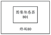
图8为本申请实施例提供的一种可选的终端的结构示意图,如图8所示,终端80包括上述实施例所述的图像传感器801。FIG. 8 is a schematic structural diagram of an optional terminal provided by an embodiment of the present application. As shown in FIG. 8 , the terminal 80 includes the
本申请实施例所记载的技术方案之间,在不冲突的情况下,可以任意组合。The technical solutions described in the embodiments of the present application may be combined arbitrarily if there is no conflict.
在本申请所提供的几个实施例中,应该理解到,所揭露的方法和智能设备,可以通过其它的方式实现。以上所描述的设备实施例仅仅是示意性的,例如,所述单元的划分,仅仅为一种逻辑功能划分,实际实现时可以有另外的划分方式,如:多个单元或组件可以结合,或可以集成到另一个系统,或一些特征可以忽略,或不执行。另外,所显示或讨论的各组成部分相互之间的耦合、或直接耦合、或通信连接可以是通过一些接口,设备或单元的间接耦合或通信连接,可以是电性的、机械的或其它形式的。In the several embodiments provided in this application, it should be understood that the disclosed method and smart device may be implemented in other manners. The device embodiments described above are only illustrative. For example, the division of the units is only a logical function division. In actual implementation, there may be other division methods. For example, multiple units or components may be combined, or Can be integrated into another system, or some features can be ignored, or not implemented. In addition, the coupling, or direct coupling, or communication connection between the components shown or discussed may be through some interfaces, and the indirect coupling or communication connection of devices or units may be electrical, mechanical or other forms. of.
上述作为分离部件说明的单元可以是、或也可以不是物理上分开的,作为单元显示的部件可以是、或也可以不是物理单元,即可以位于一个地方,也可以分布到多个网络单元上;可以根据实际的需要选择其中的部分或全部单元来实现本实施例方案的目的。The unit described above as a separate component may or may not be physically separated, and the component displayed as a unit may or may not be a physical unit, that is, it may be located in one place or distributed to multiple network units; Some or all of the units may be selected according to actual needs to achieve the purpose of the solution in this embodiment.
另外,在本申请各实施例中的各功能单元可以全部集成在一个第二处理单元中,也可以是各单元分别单独作为一个单元,也可以两个或两个以上单元集成在一个单元中;上述集成的单元既可以采用硬件的形式实现,也可以采用硬件加软件功能单元的形式实现。In addition, each functional unit in each embodiment of the present application may all be integrated into one second processing unit, or each unit may be separately used as a unit, or two or more units may be integrated into one unit; The above-mentioned integrated unit may be implemented in the form of hardware, or may be implemented in the form of hardware plus software functional units.
以上所述,仅为本申请的具体实施方式,但本申请的保护范围并不局限于此,任何熟悉本技术领域的技术人员在本申请揭露的技术范围内,可轻易想到变化或替换,都应涵盖在本申请的保护范围之内。The above are only specific embodiments of the present application, but the protection scope of the present application is not limited to this. should be covered within the scope of protection of this application.
Claims (9)
Priority Applications (1)
| Application Number | Priority Date | Filing Date | Title |
|---|---|---|---|
| CN201910329816.1A CN110049261B (en) | 2019-04-23 | 2019-04-23 | Pixel structure, image sensor and terminal |
Applications Claiming Priority (1)
| Application Number | Priority Date | Filing Date | Title |
|---|---|---|---|
| CN201910329816.1A CN110049261B (en) | 2019-04-23 | 2019-04-23 | Pixel structure, image sensor and terminal |
Publications (2)
| Publication Number | Publication Date |
|---|---|
| CN110049261A CN110049261A (en) | 2019-07-23 |
| CN110049261B true CN110049261B (en) | 2022-04-12 |
Family
ID=67278740
Family Applications (1)
| Application Number | Title | Priority Date | Filing Date |
|---|---|---|---|
| CN201910329816.1A Expired - Fee Related CN110049261B (en) | 2019-04-23 | 2019-04-23 | Pixel structure, image sensor and terminal |
Country Status (1)
| Country | Link |
|---|---|
| CN (1) | CN110049261B (en) |
Families Citing this family (6)
| Publication number | Priority date | Publication date | Assignee | Title |
|---|---|---|---|---|
| CN110505422B (en) * | 2019-08-20 | 2022-01-11 | Oppo广东移动通信有限公司 | CIS and terminal |
| CN110475083B (en) * | 2019-08-26 | 2021-12-14 | Oppo广东移动通信有限公司 | A pixel structure, image sensor and terminal |
| CN110493504B (en) * | 2019-08-29 | 2021-07-30 | Oppo广东移动通信有限公司 | Image Sensors, Imaging Systems and Terminals |
| CN110677606B (en) * | 2019-09-16 | 2022-06-10 | Oppo广东移动通信有限公司 | A pixel structure, CIS and terminal |
| CN110854145A (en) * | 2019-11-01 | 2020-02-28 | Oppo广东移动通信有限公司 | A pixel structure, image sensor and terminal |
| CN110797366A (en) * | 2019-11-14 | 2020-02-14 | Oppo广东移动通信有限公司 | Pixel structure, complementary metal oxide semiconductor image sensor and terminal |
Citations (5)
| Publication number | Priority date | Publication date | Assignee | Title |
|---|---|---|---|---|
| CN101459185A (en) * | 2007-12-11 | 2009-06-17 | 三星电子株式会社 | Photodiodes, image sensing devices and image sensors |
| CN101592751A (en) * | 2008-05-30 | 2009-12-02 | 佳能株式会社 | Light filter |
| CN102110703A (en) * | 2009-12-28 | 2011-06-29 | 索尼公司 | Semiconductor device and electronic apparatus |
| CN102510450A (en) * | 2011-10-17 | 2012-06-20 | 北京瑞澜联合通信技术有限公司 | Image sensor, pick-up device and image data generation method |
| CN104580941A (en) * | 2015-02-02 | 2015-04-29 | 联想(北京)有限公司 | Light sensing device and image output method |
Family Cites Families (4)
| Publication number | Priority date | Publication date | Assignee | Title |
|---|---|---|---|---|
| FR2983348B1 (en) * | 2011-11-29 | 2014-07-25 | Thales Sa | OPTICAL DETECTOR BLOCK |
| CN102664185A (en) * | 2012-06-01 | 2012-09-12 | 上海中科高等研究院 | CMOS (Complementary Metal Oxide Semiconductor) image sensor and production method thereof |
| US20170173262A1 (en) * | 2017-03-01 | 2017-06-22 | François Paul VELTZ | Medical systems, devices and methods |
| CN113158868A (en) * | 2017-08-17 | 2021-07-23 | 深圳信炜科技有限公司 | Photosensitive module, display module and electronic equipment |
-
2019
- 2019-04-23 CN CN201910329816.1A patent/CN110049261B/en not_active Expired - Fee Related
Patent Citations (5)
| Publication number | Priority date | Publication date | Assignee | Title |
|---|---|---|---|---|
| CN101459185A (en) * | 2007-12-11 | 2009-06-17 | 三星电子株式会社 | Photodiodes, image sensing devices and image sensors |
| CN101592751A (en) * | 2008-05-30 | 2009-12-02 | 佳能株式会社 | Light filter |
| CN102110703A (en) * | 2009-12-28 | 2011-06-29 | 索尼公司 | Semiconductor device and electronic apparatus |
| CN102510450A (en) * | 2011-10-17 | 2012-06-20 | 北京瑞澜联合通信技术有限公司 | Image sensor, pick-up device and image data generation method |
| CN104580941A (en) * | 2015-02-02 | 2015-04-29 | 联想(北京)有限公司 | Light sensing device and image output method |
Also Published As
| Publication number | Publication date |
|---|---|
| CN110049261A (en) | 2019-07-23 |
Similar Documents
| Publication | Publication Date | Title |
|---|---|---|
| CN110049261B (en) | Pixel structure, image sensor and terminal | |
| CN110085611B (en) | Pixel unit, image sensor, image processing method, and storage medium | |
| US8405748B2 (en) | CMOS image sensor with improved photodiode area allocation | |
| US8704934B2 (en) | Solid-state imaging device having pixels arranged in a honeycomb structure | |
| CN101281921B (en) | Solid-state imaging device and imaging device | |
| CN104412580B (en) | Color image sensor and camera head | |
| CN110112155B (en) | Pixel unit, image sensor, image processing method, and storage medium | |
| CN110164895B (en) | CMOS image sensor, image processing method and storage medium | |
| WO2014150856A1 (en) | Array camera implementing quantum dot color filters | |
| CN110650301B (en) | Image sensor, imaging method and device | |
| KR20140041679A (en) | Multi scene depth photo sensitive device, system thereof, scene depth expanding method, and optical imaging system | |
| US9219894B2 (en) | Color imaging element and imaging device | |
| CN110061019B (en) | Complementary metal oxide image sensor, image processing method and storage medium | |
| CN111739900A (en) | Image sensor, image sensing method, chip and electronic device | |
| CN114666469B (en) | Image processing device, method and lens module with image processing device | |
| CN116417483A (en) | A kind of spectral imaging chip and preparation method of spectral imaging chip | |
| WO2012169136A1 (en) | Color separation filter array, solid-state imaging element, imaging device, and display device | |
| US8400538B2 (en) | Apparatus and method for capturing images | |
| CN110505422B (en) | CIS and terminal | |
| CN110505419B (en) | A pixel structure, image sensor and terminal | |
| CN110677606B (en) | A pixel structure, CIS and terminal | |
| CN110475083B (en) | A pixel structure, image sensor and terminal | |
| CN111182247B (en) | A pixel structure, image sensor and terminal | |
| CN110418088B (en) | Pixel structure, image sensor and terminal | |
| CN110324545B (en) | Pixel structure, image sensor and terminal |
Legal Events
| Date | Code | Title | Description |
|---|---|---|---|
| PB01 | Publication | ||
| PB01 | Publication | ||
| SE01 | Entry into force of request for substantive examination | ||
| SE01 | Entry into force of request for substantive examination | ||
| GR01 | Patent grant | ||
| GR01 | Patent grant | ||
| CF01 | Termination of patent right due to non-payment of annual fee | ||
| CF01 | Termination of patent right due to non-payment of annual fee |
Granted publication date: 20220412 |