Testing device and testing method for CCD controller
Technical Field
The invention belongs to the technical field of CCD detector testing, and relates to a testing device and a testing method for a CCD controller.
Background
In the field of photoelectric detectors, scientific grade CCD detectors are widely used in numerous fields such as astronomy, medicine, etc. due to their advantages of high quantum efficiency, ultra-low readout noise, high resolution, wide spectral response range, etc. A typical scientific grade CCD detector system includes a scientific grade CCD detector, a CCD controller, and user control interface software. The basic function of the CCD controller is to provide the scientific CCD detector with clock signals and bias signals required for its operation, and to amplify and sample the video signals output by the scientific CCD detector. Because the scientific grade CCD detector is expensive in manufacturing cost and easy to damage, and strict operation specifications need to be followed during installation, before the scientific grade CCD detector is installed, the functions and performances of all parts of circuits in the controller system need to be ensured to meet the requirements through detailed tests, so that the scientific grade CCD detector is prevented from being frequently disassembled and assembled during debugging, and meanwhile, the performance index of the CCD controller can be evaluated before the CCD is not installed.
At present, a scientific grade CCD detector system is a core device in the field of astronomical imaging, and astronomical observation sites are mostly established in places with high seeing, good atmospheric conditions and the like, such as south Pole. This requires that the controller system be capable of operating in extreme cold conditions, and it is therefore highly desirable to test the controller system for low temperature reliability quickly and easily.
The test system designed by the invention meets the test requirements of different types of scientific-grade CCD controllers, can test and evaluate the functions and the performances of circuits of all parts of the controller under the condition of not installing scientific-grade CCD detectors, and can test different scientific-grade CCD controllers by replacing different interface adapter plates.
Disclosure of Invention
The invention aims to provide a testing device and a testing method for a CCD controller, which solve the problems that the function and the performance of each part of a circuit of the controller can be tested under the condition that a scientific grade CCD detector needs to be installed in the prior art, the testing compatibility of the CCD controller is poor, the debugging is complicated and the like.
The purpose of the invention can be realized by the following technical scheme:
a testing device for a CCD controller comprises testing system operation software, CCD controller operation software, an interface adapter plate and a testing system;
the test system operation software is connected with an FPGA chip in the test system through a USB/optical fiber interface, is used for sending a control instruction to the FPGA chip and receiving test data sent by the FPGA chip, is in network communication connection with the CCD controller operation software, and is used for sending the control instruction to the CCD controller operation software so as to control the CCD controller to operate according to test requirements;
the CCD controller operation software is connected with the CCD controller, controls the CCD controller to generate a clock and bias voltage and controls the video waveform sampling circuit to collect waveforms;
the interface adapter plate comprises a first connector and a second connector connected with the first connector, the first connector is connected with the CCD controller, and the second connector is connected with a plurality of test interfaces on the test system;
the testing system is used for testing a clock circuit, a bias circuit, a video sampling circuit, a temperature sampling circuit, power supply voltage, a shutter control signal and a fan control signal of the CCD controller, storing tested data, comparing the stored tested data with data operated by software of the CCD controller, and generating a test report.
Furthermore, the test system comprises an FPGA chip, a USB/optical fiber interface, a clock test circuit, a bias test circuit, a video waveform generator, a multi-channel gate, a multi-channel analog-to-digital converter, a first voltage division circuit, a second voltage division circuit, a first comparator, a second comparator, a power supply module, a serial communication module and a plurality of test interface components, wherein the test interface components comprise a first test interface, a second test interface, a third test interface, a fourth test interface, a fifth test interface, a sixth test interface and a seventh test interface;
the FPGA chip is respectively connected with the USB/optical fiber interface, the clock test circuit, the bias test circuit, the video waveform generator, the multi-channel analog-to-digital converter, the first voltage division circuit, the second voltage division circuit, the first comparator, the second comparator and the serial port communication module;
one end of the first test interface, one end of the second test interface and one end of the third test interface are connected with the second plug connector on the interface adapter plate, the other end of the first test interface is connected with the input end of the clock test circuit, the other end of the second test interface is connected with the input end of the bias voltage test circuit, and the other end of the third test interface is connected with the output end of the video waveform generator.
Furthermore, the CCD controller comprises a clock circuit, a bias circuit, a video waveform sampling circuit, a temperature sampling circuit, a power supply voltage acquisition circuit, a shutter control signal acquisition circuit and a fan control signal acquisition circuit, wherein the clock circuit, the bias circuit and the video waveform sampling circuit are respectively connected with the interface adapter plate;
the temperature sampling circuit is connected with the output end of the multi-path gate through a fourth test interface;
the power supply voltage acquisition circuit is connected with the input end of the multi-channel analog-to-digital converter through a fifth test interface;
the shutter control signal acquisition circuit is connected with the input end of the first voltage division circuit through a sixth test interface, and the output end of the first voltage division circuit is connected with the input end of the first comparator;
the fan control signal acquisition circuit is connected with the input end of the second voltage division circuit through the seventh test interface, and the output end of the second voltage division circuit is connected with the input end of the second comparator.
Further, when a temperature sampling circuit in the CCD controller is tested, the temperature sensor interface is connected to the test interface 4 through a flat cable, the resistance value of the multi-channel gate 1 which is connected is changed through test system operation software, the corresponding resistance value is obtained through the temperature sampling circuit sampling resistor, the obtained resistance value is converted into a temperature value, and the converted temperature value is compared with the temperature value which is theoretically corresponding to the resistor, so that whether the sampling of the temperature sampling circuit is accurate or not is verified;
when testing the power supply voltage in the CCD controller, each path of power supply voltage is accessed to the test interface 5 through a cable, the channel of the multichannel ADC to be tested is selected through the test system operation software, the voltage test result of the channel is obtained, the test result is displayed on a user interface, the voltage value is compared with the configuration value of the CCD controller, and whether the voltage is normal or not is judged.
When testing the shutter control signal in the CCD controller, the shutter control signal is accessed into the test interface 6 through the coaxial cable, the test system operation software appoints the CCD controller control software through the network to send a corresponding shutter opening and closing command to the CCD controller, the actual high level duration time of the shutter signal is tested through the test interface 6, and the test result is uploaded to the test system operation software, and in the test system operation software, whether the opening and closing of the shutter control signal are normal is judged by comparing the appointed shutter opening time value with the shutter signal high level duration time obtained through actual measurement.
When testing a fan control signal in a CCD controller, the fan control signal is accessed into a test interface 7 through a flat cable, test system operation software designates the CCD controller control software through a network to send a corresponding fan rotating speed control signal to the CCD controller, the test interface 7 tests the actual high level duration and low level duration of the fan control signal, the actual duty ratio of the fan control signal is calculated, and a test result is uploaded to the test system operation software, and in the test system operation software, whether the fan control signal is normal or not is judged by comparing the duty ratio value corresponding to the designated fan rotating speed parameter with the duty ratio value obtained through actual measurement.
Furthermore, the clock test circuit comprises a load capacitor, a digital-to-analog converter, an operational amplifier, a plurality of voltage division circuits and a high-speed comparator, wherein a plurality of paths of clock signals generated by the CCD controller are introduced into the test interface 1 through an interface adapter plate, the test system provides 20 paths of clock test interfaces, a load capacitor network is used for simulating the load of the CCD detector, each path of clock signals in the clock circuit is connected with one end of each voltage division circuit through the load capacitor, the other end of each voltage division circuit is connected with the high-speed comparator, the reference voltage of the high-speed comparator is generated by the digital-to-analog converter (DAC) and is output after operational amplification, and the output end of the high-speed comparator is connected with the FPGA;
the clock test circuit comprises a time sequence test part and a clock voltage test part, in the time sequence test process, test system operation software designates CCD controller operation software through a network to set CCD time sequence parameters of a CCD controller and output the CCD time sequence parameters, the test system outputs the cycle, duty ratio and phase relation of all clock signals through sampling each path of comparator, test results are stored and displayed on the test system operation software, and the cycle, duty ratio and phase of the clock signals are respectively compared with the preset CCD time sequence parameters one by one to judge whether the time sequences of the clock signals are completely consistent;
in the process of testing the clock voltage, the testing system operating software appoints the CCD controller operating software through a network to set CCD clock voltage parameters of the CCD controller and control the CCD controller to output, the testing system respectively samples the output of each high-speed comparator, sets the maximum reference voltage and the minimum reference voltage of the high-speed comparators, changes the reference voltage of the high-speed comparators through a bisection method according to the sampling result, gradually approaches the voltage of a clock signal at the input end of the comparator, sequentially obtains the high and low levels of each circuit of clock, stores and displays the testing result on the testing system operating software, compares the voltage of the clock signal with a preset CCD voltage parameter configuration value, and evaluates whether the clock circuit voltage parameters of the CCD controller are within an allowable error range through the comparison of the set parameter value and the testing value.
Furthermore, the bias test circuit comprises a multi-channel gate, a single-channel high-speed analog-to-digital converter and a plurality of voltage division circuits, a multi-channel bias signal generated by the CCD controller is introduced into the test interface 2 through the interface adapter plate, the test system provides 8 channels of bias test interfaces, and the bias signal enters the multi-channel gate through the voltage division circuits. The multi-channel gate is controlled by the FPGA, the gated bias signal is sampled by a single-channel high-speed analog-to-digital converter, and the bias test circuit comprises a bias value test and a bias quality test;
in the bias voltage test process, test system operation software designates CCD controller operation software through a network to control the CCD controller to generate bias voltage, the test system operation software selects the bias voltage to be tested, the sampling times are set and bias voltage test commands are sent, the voltage value information of the bias voltage is sampled for multiple times by the high-speed analog-to-digital converter and is uploaded to the test system operation software for storage, the average value and the mean square value are calculated and analyzed, and whether the voltage value and the voltage quality of a bias voltage circuit of the CCD controller are within an allowable range is evaluated through comparison of bias voltage setting parameter values and measured values.
Furthermore, the video waveform generator comprises a high-speed digital-to-analog converter DAC, a low-pass filtering module and an operational amplifier, the FPGA controls the high-speed digital-to-analog converter DAC to output differential voltage signals Vp and Vn, the output differential voltage signals are filtered by the low-pass filtering module to remove high-frequency noise, the operational amplifier converts the differential voltage signals into single-ended signals to be output, meanwhile, a true random number generator designed based on the jitter of an oscillation ring in the FPGA as a random source is used for outputting true random numbers, the true random numbers are superposed on the data codes of the digital-to-analog converter DAC to output video signals serving as inherent noise of an analog CCD detector, a test system simulates the video signals output by an actual CCD detector through a video waveform sampling circuit, and the video signals are introduced into the CCD controller through an interface adapter plate and a test interface 3 in sequence;
the video waveform generator comprises a function test and a performance test, in the function test, the test system control software sets the video waveform generator to generate an image with characteristics, and appoints the CCD controller operation software to set corresponding reading rate and gain parameters through a network and sends an exposure command, and after the CCD controller finishes acquiring an image, a user judges whether a video waveform sampling circuit of the CCD controller is normal in function or not by judging whether the acquired image is completely consistent with a set characteristic pattern or not;
in the performance test, a true random number generator module in an FPGA chip superposes random noises with different noise amounts in a video signal, sampling is carried out through a video waveform sampling circuit, and a user compares the mean square error of pixel values sampled by the video waveform sampling circuit with a theoretical value generated by the video waveform generator to verify whether the performance of the video sampling circuit is within an allowable error range.
A test method for a CCD controller, comprising the steps of:
step S1, generating and testing a clock circuit in the CCD controller;
the test system operation software controls a multi-channel clock signal generated by a CCD controller through CCD control software and introduces the multi-channel clock signal into the test system through a patch panel, the clock signal sequentially enters a comparator through a load capacitor and a voltage division circuit, the output of the comparator is connected with an FPGA chip, the reference voltage of the comparator is generated by a digital-to-analog converter (DAC) and is output after being amplified by an operational amplifier, and the clock circuit test is divided into a time sequence test part and a clock voltage test part. The time sequence test comprises testing the period, duty ratio and phase relation of each path of clock, and the clock voltage test comprises testing the high and low levels of each path of clock; in the testing process, the CCD controller outputs corresponding CCD time sequence through parameters set by user control software, the testing system sends corresponding testing commands through the testing system operating software, then the testing results are recorded and displayed on a user interface, and the testing results are compared with the parameters sent by the CCD controller one by one;
step S2, generating and testing a bias circuit in the CCD controller;
the test system operation software controls a multi-path bias signal generated by the CCD controller through the CCD control software and introduces the multi-path bias signal into the test system through the interface adapter plate, the bias signal enters a multi-path gate through a voltage division circuit, the multi-path gate is controlled by the FPGA chip, and the gated bias signal is sampled through an analog-to-digital converter (ADC);
the bias circuit test is divided into a bias value test part and a bias mean square error test part, in the test process, a test system selects bias to be tested through test system operating software, sets sampling times and sends a bias test command, then the bias value and the bias quality are displayed on a user interface and compared with parameters set by a CCD (charge coupled device) controller, and a user can judge whether the performance of the bias circuit meets the requirements or not through the magnitude of the bias quality;
step S3, testing the video sampling circuit;
the testing system simulates a video signal output by an actual CCD detector through a video waveform generator, the video signal is introduced into the CCD controller through an interface adapter plate, and the testing system operating software controls the CCD controller through the CCD controller operating software to sample the video signal by using a video sampling circuit;
the video sampling circuit test is divided into a function test part and a performance test part, in the function test, a test system sets voltage parameters of video waveforms through operation software, simultaneously accesses CCD controller operation software to set corresponding reading rate and gain parameters of a CCD controller, sends an exposure command, and automatically judges whether the function of the sampling circuit is correct or not by comparing video signal data set by the test system with pixel values sampled by a sampling circuit of the CCD controller;
in the performance test, a test system enables a True Random Number Generator (TRNG) to generate random noise in an analog mode, different random noise is superposed in a video signal, and a CCD controller carries out sampling through a video waveform sampling circuit. The testing system verifies whether the performance of the video sampling circuit meets the requirement or not by comparing the mean square error of the pixel values sampled by the video sampling circuit with a theoretical value;
step S4, testing a temperature sampling circuit of the CCD controller;
the basic principle of a temperature sampling circuit of the CCD controller is that an analog-to-digital converter ADC chip is used for sampling the resistance value of a temperature sensor, the resistance value is converted into temperature in a lookup table mode, and a test system connects a plurality of high-precision resistors with different resistance values to a test interface through a multi-channel gate;
in the test of the temperature sampling circuit, the temperature sensor interface of the CCD controller is connected to the corresponding test interface of the test system through the flat cable, the test system selects the resistance value to be switched on through the operation software of the test system, and the temperature sampled by the temperature sampling circuit in the CCD controller is compared with the temperature corresponding to the resistance, so that whether the temperature sampling circuit is accurate in sampling can be verified;
step S5, testing the power supply voltage of the CCD controller;
each path of power supply of the CCD controller is led into a test interface of the test system through a cable, and enters the multichannel analog-to-digital converter ADC after passing through the voltage division circuit. In the power supply voltage test, a test system selects a channel to be tested through CCD controller operation software, sends a corresponding test command, stores a test result and displays the test result on a user interface, and compares the voltage value with a numerical value in the CCD controller software to judge whether the power supply voltage is normal or not;
step S6, testing a shutter control signal and a fan control signal of the CCD controller;
the shutter control signal of the CCD controller controls the opening time of the shutter, and the shutter control signal is introduced into the test system through the coaxial cable and is tested for the high level time. A fan control signal of the CCD controller controls the rotating speed of the fan, and the fan control signal is introduced into the test system through a flat cable and the duty ratio of the fan control signal is tested;
the shutter signal and the fan signal of the test system respectively enter the comparator after passing through the voltage division circuit. In the test, the test system sets the corresponding exposure time and the fan rotating speed percentage through the CCD controller operation software, selects the signal to be tested through the CCD controller operation software, sends the corresponding test command, then stores the test result, displays the test result on a user interface, and automatically judges whether the signal is normally generated with a set value;
all test data is stored and the stored test data is compared to the data of the CCD controller software operation and a test report is generated.
The invention has the beneficial effects that:
the testing device for the CCD controller provided by the invention can test the clock circuit, the bias circuit, the video sampling circuit, the temperature sampling circuit, the power supply voltage, the shutter control signal, the fan control signal and the like of the CCD controller by the testing system in combination with the testing system operating software and the CCD controller operating software, so as to test and evaluate the functions and the performances of all circuits of the CCD controller under the condition of not installing a scientific grade CCD detector, and can test different CCD controllers by replacing different interface adapter plates, thereby being convenient for improving the performances of all circuits of the controller and having the characteristics of strong testing compatibility and good debugging convenience.
Drawings
In order to more clearly illustrate the technical solutions of the embodiments of the present invention, the drawings used in the description of the embodiments will be briefly introduced below, and it is obvious that the drawings in the following description are only some embodiments of the present invention, and it is obvious for those skilled in the art that other drawings can be obtained according to the drawings without creative efforts.
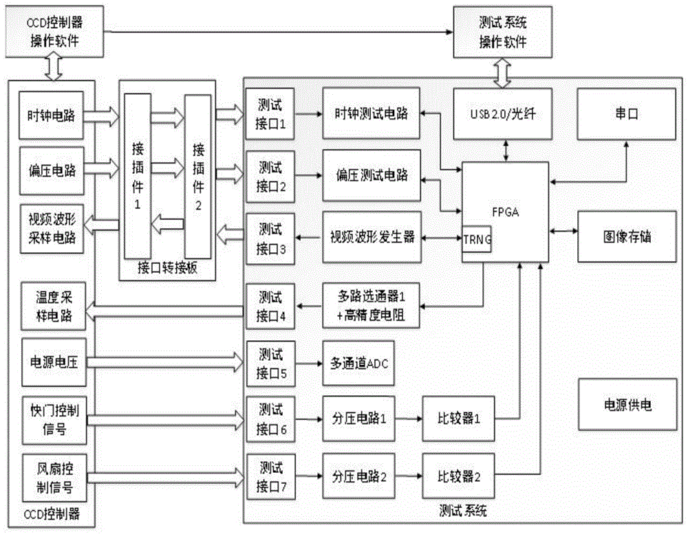
FIG. 1 is a schematic diagram of a testing apparatus for a CCD controller according to the present invention;
FIG. 2 is a schematic diagram of a clock test circuit according to the present invention;
FIG. 3 is a schematic diagram of a bias test circuit according to the present invention;
FIG. 4 is a schematic diagram of a video waveform generator according to the present invention.
Detailed Description
The technical solutions in the embodiments of the present invention will be clearly and completely described below with reference to the drawings in the embodiments of the present invention, and it is obvious that the described embodiments are only a part of the embodiments of the present invention, and not all of the embodiments. All other embodiments, which can be derived by a person skilled in the art from the embodiments given herein without making any creative effort, shall fall within the protection scope of the present invention.
Referring to fig. 1 to 4, a testing apparatus for a CCD controller includes a testing system operating software, a CCD controller operating software, an interface adapter board, and a testing system;
the testing system operating software is used as a control core of the whole system, is connected with an FPGA chip in the testing system through a USB/optical fiber interface and is used for sending a control instruction to the FPGA chip and receiving test data sent by the FPGA chip, and is in network communication connection with the CCD controller operating software and is used for sending the control instruction to the CCD controller operating software so as to control the CCD controller to operate according to the test requirement;
the CCD controller operation software is connected with the CCD controller, controls the CCD controller to generate a clock and bias voltage, and controls the video waveform sampling circuit to collect waveforms and the like.
The interface adapter plate comprises a first connector and a second connector connected with the first connector, the first connector is connected with the CCD controller, and the second connector is connected with a plurality of test interfaces on the test system;
the test system comprises an FPGA chip, a USB/optical fiber interface, a clock test circuit, a bias test circuit, a video waveform generator, a multi-channel gate, a multi-channel analog-to-digital converter (ADC), a first voltage division circuit, a second voltage division circuit, a first comparator, a second comparator, a power supply module, a serial communication module and a plurality of test interface components, wherein the test interface components comprise a first test interface, a second test interface, a third test interface, a fourth test interface, a fifth test interface, a sixth test interface and a seventh test interface;
the CCD controller comprises a clock circuit, a bias circuit, a video waveform sampling circuit, a temperature sampling circuit, a power supply voltage acquisition circuit, a shutter control signal acquisition circuit and a fan control signal acquisition circuit, wherein the clock circuit, the bias circuit and the video waveform sampling circuit are respectively connected with an interface adapter plate;
the second plug connector on the interface adapter plate is respectively connected with a first test interface, a second test interface and a third test interface, the first test interface is connected with the input end of the clock test circuit, the second test interface is connected with the input end of the bias test circuit, and the third test interface is connected with the output end of the video waveform generator;
the temperature sampling circuit is connected with the output end of the multi-path gate through a fourth test interface;
the power supply voltage acquisition circuit is connected with the input end of the multi-channel analog-to-digital converter through a fifth test interface;
the shutter control signal acquisition circuit is connected with the input end of the first voltage division circuit through a sixth test interface, and the output end of the first voltage division circuit is connected with the input end of the first comparator;
the fan control signal acquisition circuit is connected with the input end of the second voltage division circuit through the seventh test interface, and the output end of the second voltage division circuit is connected with the input end of the second comparator.
The user can connect corresponding test interfaces according to the test requirements of different CCD controllers to test the sampling circuit connected with the CCD controllers.
In the test of the temperature sampling circuit of the CCD controller, the temperature sensor interface is connected to the test interface 4 through the flat cable, the high-precision resistance value connected with the multi-channel gate 1 is changed through the operation software of the test system, the high-precision resistance is sampled through the temperature sampling circuit to obtain the corresponding resistance value, the obtained resistance value is converted into a temperature value, and the converted temperature value is compared with the temperature value theoretically corresponding to the high-precision resistance to verify whether the sampling of the temperature sampling circuit is accurate. In the power supply voltage test of the CCD controller, each path of power supply voltage is accessed to the test interface 5 through a cable, a channel of the multichannel ADC to be tested is selected through test system operation software, a voltage test result of the channel is obtained, the test result is displayed on a user interface, and the voltage value is compared with a configuration value of the CCD controller, so that a user can conveniently judge whether the voltage is normal or not. In the test of the shutter control signal of the CCD controller, the shutter control signal is accessed into a test interface 6 through a coaxial cable, test system operation software designates the CCD controller control software through a network to send a corresponding shutter opening and closing command to the CCD controller, the actual high level duration time of the shutter signal is tested through the test interface 6, and a test result is uploaded to the test system operation software. In the fan control signal test of the CCD controller, a fan control signal is accessed to a test interface 7 through a flat cable, test system operation software designates the CCD controller control software through a network to send a corresponding fan rotating speed control signal to the CCD controller, the actual high level duration and low level duration of the fan control signal are tested through the test interface 7, the actual duty ratio of the fan control signal is calculated, and a test result is uploaded to the test system operation software, and in the test system operation software, whether the fan control signal is normal or not is judged by comparing whether the duty ratio corresponding to the designated fan rotating speed parameter is consistent with the duty ratio obtained through actual measurement or not.
As shown in fig. 2, the clock test circuit includes a load capacitor, a digital-to-analog converter (DAC), an operational amplifier, a plurality of voltage dividing circuits, and a high-speed comparator, wherein a plurality of clock signals generated by the CCD controller are introduced into the test interface 1 through the interface adapter plate, the test system provides 20 clock test interfaces, the load capacitor network is used to simulate the load of the CCD detector, each clock signal in the clock circuit is connected to one end of a voltage dividing circuit through the load capacitor, and the other end of the voltage dividing circuit is connected to a high-speed comparator. The reference voltage of the high-speed comparator is generated by a digital-to-analog converter (DAC), amplified by an operational amplifier and then output, and the output end of the high-speed comparator is connected with the FPGA.
The clock test circuit comprises a time sequence test part and a clock voltage test part, in the time sequence test process, test system operation software designates CCD controller operation software through a network to set CCD time sequence parameters of a CCD controller and output the CCD time sequence parameters, the test system outputs the cycle, duty ratio and phase relation of all clock signals through sampling each path of comparator, test results are stored and displayed on the test system operation software, and the cycle, duty ratio and phase of the clock signals are respectively compared with the preset CCD time sequence parameters one by one to judge whether the time sequences of the clock signals are completely consistent; in the process of testing the clock voltage, the testing system operating software appoints the CCD controller operating software through a network to set CCD clock voltage parameters of the CCD controller and control the CCD controller to output, the testing system respectively samples the output of each high-speed comparator, sets the maximum reference voltage and the minimum reference voltage of the high-speed comparators, changes the reference voltage of the high-speed comparators through a bisection method according to the sampling result, gradually approaches the voltage of a clock signal at the input end of the comparator, so as to sequentially obtain the high and low levels of each circuit of clock, stores and displays the testing result on the testing system operating software, compares the voltage of the clock signal with a preset CCD voltage parameter configuration value, evaluates whether the clock circuit voltage parameters of the CCD controller are within an allowable error range through the comparison of the set parameter value and the testing value, wherein the allowable error range can be set in the testing system operating software, such as 1% or 5%.
As shown in fig. 3, the bias test circuit includes a multi-way gate, a single-channel high-speed analog-to-digital converter, and a plurality of voltage dividing circuits, the multi-way bias signal generated by the CCD controller is introduced into the test interface 2 through the interface adapter board, the test system provides 8-way bias test interface, and the bias signal enters the multi-way gate through the voltage dividing circuits. The multi-channel gate is controlled by the FPGA, the gated bias voltage signal is sampled by the single-channel high-speed analog-to-digital converter, and the bias voltage test circuit comprises a bias voltage value test and a bias voltage quality test, wherein the bias voltage value is represented by an average value of multiple measurement results, and the bias voltage quality is represented by a mean square error value of the multiple measurement results.
In the bias test process, the test system operating software designates the CCD controller operating software to control the CCD controller to generate bias voltage through a network, the test system operating software selects the bias voltage to be tested, the sampling times are set and bias voltage test commands are sent, the voltage value information of the bias voltage is sampled by the high-speed analog-to-digital converter for multiple times and uploaded to the test system operating software for storage, the average value and the mean square value are statistically analyzed, the average value represents the bias voltage measured value, the mean square value represents the bias voltage quality, whether the bias voltage circuit voltage value and the voltage quality of the CCD controller are within an allowable range is evaluated through the comparison of the bias voltage setting parameter value and the measured value, and the allowable error range can be set in the test system operating software, such as 1% or 5%.
As shown in fig. 4, the video waveform generator includes a high-speed digital-to-analog converter DAC, a low-pass filter module and an operational amplifier, the FPGA controls the high-speed digital-to-analog converter DAC to output differential voltage signals Vp and Vn, the output differential voltage signals are filtered by the low-pass filter module to remove high-frequency noise, the operational amplifier converts the differential voltage signals into single-ended signals and outputs the single-ended signals, meanwhile, the true random number generator designed based on the jitter of an oscillation ring inside the FPGA as a random source is used to output true random numbers, the video signals output after being superimposed on DAC data codes of the digital-to-analog converter are used as inherent noise of the analog CCD detector, the test system simulates video signals output by an actual CCD detector through a video waveform sampling circuit, and the video signals are introduced into the CCD controller through an interface adapter plate and a test interface 3 in sequence.
The video waveform generator provides function test and performance test, in the function test, the test system control software sets the video waveform generator to generate images with certain characteristics, such as uniform flat field images or regular stripe patterns, and appoints the CCD controller operation software to set corresponding parameters such as reading speed, gain and the like through a network, and sends an exposure command, after the CCD controller collects an image, a user judges whether the obtained image is completely consistent with the set characteristic patterns or not, so as to judge whether a video waveform sampling circuit of the CCD controller is normal in function or not. In the performance test, a true random number generator module (TRNG) in an FPGA chip superimposes random noise with different amounts of noise on a video signal, sampling is performed by a video waveform sampling circuit, and a user compares a mean square error of pixel values sampled by the video waveform sampling circuit with a theoretical value generated by the video waveform generator to verify whether the performance of the video sampling circuit is within an allowable error range, wherein the allowable error range can be set in test system operating software, such as 1% or 5%.
A test method for a CCD controller, comprising the steps of:
step S1, generating and testing a clock circuit in the CCD controller;
the test system operation software controls a multi-channel clock signal generated by a CCD controller through CCD control software and introduces the multi-channel clock signal into the test system through a patch panel, the clock signal sequentially enters a comparator through a load capacitor and a voltage division circuit, the output of the comparator is connected with an FPGA chip, the reference voltage of the comparator is generated by a digital-to-analog converter (DAC) and is output after being amplified by an operational amplifier, and the clock circuit test is divided into a time sequence test part and a clock voltage test part. The time sequence test comprises testing the period, duty ratio and phase relation of each path of clock, and the clock voltage test comprises testing the high and low levels of each path of clock. In the testing process, the CCD controller outputs corresponding CCD time sequence through parameters set by user control software, the testing system sends corresponding testing commands through the testing system operating software, then the testing results are recorded and displayed on a user interface, and the testing results are compared with the parameters sent by the CCD controller one by one.
Step S2, generating and testing a bias circuit in the CCD controller;
the test system operation software controls a multi-path bias signal generated by the CCD controller through the CCD control software and introduces the test system through the interface adapter plate, the bias signal enters the multi-path gate through the voltage division circuit, the multi-path gate is controlled by the FPGA chip, and the gated bias signal is sampled through the ADC.
The bias circuit test is divided into two parts of bias value test and bias mean square error test, in the test process, the test system selects the bias to be tested through the test system operating software, sets the sampling times and sends the bias test command, then the bias value and the bias quality are displayed on a user interface and compared with the bias value and the parameters set by the CCD controller, and the user can judge whether the performance of the bias circuit meets the requirements or not through the magnitude of the bias quality.
Step S3, testing the video sampling circuit;
the testing system simulates a video signal output by an actual CCD detector through a video waveform generator, the video signal is introduced into the CCD controller through an interface adapter plate, and the testing system operating software controls the CCD controller through the CCD controller operating software to sample the video signal by using a video sampling circuit.
The video sampling circuit test is divided into a function test part and a performance test part, in the function test, a test system sets voltage parameters of video waveforms through operation software, simultaneously accesses CCD controller operation software to set corresponding read-out speed, gain and other parameters of a CCD controller, sends an exposure command, and automatically judges whether the function of the sampling circuit is correct or not by comparing video signal data set by the test system with pixel values sampled by the sampling circuit of the CCD controller. In the performance test, a test system enables a True Random Number Generator (TRNG) to generate random noise in an analog mode, different random noise is superposed in a video signal, and a CCD controller carries out sampling through a video waveform sampling circuit. The testing system can verify whether the performance of the video sampling circuit meets the requirements or not by comparing the mean square error of the pixel values sampled by the video sampling circuit with a theoretical value.
Step S4, testing a temperature sampling circuit of the CCD controller;
the basic principle of the temperature sampling circuit of the CCD controller is to sample the resistance value of the temperature sensor by using an ADC chip and convert the resistance value into temperature in a lookup table mode. The test system connects a plurality of high-precision resistors with different resistance values to the test interface through the multiplexer.
In the test of the temperature sampling circuit, the temperature sensor interface of the CCD controller is connected to the corresponding test interface of the test system through the flat cable, the test system selects the resistance value to be connected through the operation software of the test system, and whether the temperature sampling circuit is accurate or not can be verified through comparing the temperature sampled by the temperature sampling circuit in the CCD controller with the temperature corresponding to the resistance.
Step S5, testing the power supply voltage of the CCD controller;
each path of power supply of the CCD controller is led into a test interface of the test system through a cable, and enters the multichannel analog-to-digital converter ADC after passing through the voltage division circuit. In the power supply voltage test, the test system selects a channel to be tested through the CCD controller operation software, sends a corresponding test command, then stores a test result and displays the test result on a user interface, and compares the voltage value with a numerical value in the CCD controller software to judge whether the power supply voltage is normal or not.
Step S6, testing a shutter control signal and a fan control signal of the CCD controller;
the shutter control signal of the CCD controller controls the opening time of the shutter, and the shutter control signal is introduced into the test system through the coaxial cable and is tested for the high level time. The fan control signal of the CCD controller controls the rotating speed of the fan, and the testing system is introduced through the flat cable and tests the duty ratio of the fan control signal.
The shutter signal and the fan signal of the test system respectively enter the comparator after passing through the voltage division circuit. In the test, the test system sets the corresponding exposure time and the fan rotating speed percentage through the CCD controller operation software, selects the signal to be tested through the CCD controller operation software, sends the corresponding test command, then stores the test result, displays the test result on the user interface, and automatically judges whether the signal is normally generated with the set value.
All test data is stored and the stored test data is compared to the data of the CCD controller software operation and a test report is generated. The test system operating software is used as a client of the CCD controller operating software to automatically control the operation of the CCD controller, and the test result and the set configuration result are stored and automatically compared to generate a test report and complete the full automation of the whole test.
The foregoing is merely exemplary and illustrative of the principles of the present invention and various modifications, additions and substitutions of the specific embodiments described herein may be made by those skilled in the art without departing from the principles of the present invention or exceeding the scope of the claims set forth herein.