CN109787494B - A voltage switching circuit and dual energy CT - Google Patents
A voltage switching circuit and dual energy CT Download PDFInfo
- Publication number
- CN109787494B CN109787494B CN201910193303.2A CN201910193303A CN109787494B CN 109787494 B CN109787494 B CN 109787494B CN 201910193303 A CN201910193303 A CN 201910193303A CN 109787494 B CN109787494 B CN 109787494B
- Authority
- CN
- China
- Prior art keywords
- voltage
- unit
- electrically connected
- filtering
- rectifying
- Prior art date
- Legal status (The legal status is an assumption and is not a legal conclusion. Google has not performed a legal analysis and makes no representation as to the accuracy of the status listed.)
- Active
Links
Images




Landscapes
- Inverter Devices (AREA)
- Dc-Dc Converters (AREA)
Abstract
Description
技术领域technical field
本发明实施例涉及电子电路技术领域,尤其涉及一种电压切换电路和双能CT。The embodiments of the present invention relate to the technical field of electronic circuits, and in particular, to a voltage switching circuit and a dual-energy CT.
背景技术Background technique
电子计算机断层扫描仪器(Computed Tomography,CT)广泛应用于医学检查、工业检测和安保检测等检测领域。随着工艺水平和计算机技术的发展,CT也得到了飞速的发展,为了得到更加准确的检测结果,双能CT应运而生。Computed tomography (Computed Tomography, CT) is widely used in medical inspection, industrial inspection and security inspection and other inspection fields. With the development of technological level and computer technology, CT has also developed rapidly. In order to obtain more accurate detection results, dual-energy CT came into being.
双能CT的工作原理为,逆变器、高压变压器、整流滤波模块组成高压发生器,高压发生器输出的电压在两个电压等级之间快变(例如,低电压等级为80kV,高电压等级为140kV),球管作为一种X射线发生源在这两个电压等级下分别射出能级能量不同的两种X射线,X射线探测器(X-ray detector)据此可以获得双能数据。以及,两个电压等级之间的切换时间越短,越有利于双能数据的分离;相反,两个电压等级之间的切换时间越长,发射的无效X射线的剂量越大,CT转一圈的有效视图数量越少。因此,更短的电压切换时间成为双能CT的高压发生器的发展趋势。其中,电压等级的切换包括高压工作模态和低压工作模态,在低压工作模态向高压工作模态切换的过程中,逆变器的电流应力可能会远大于高压发生器稳态输出时的逆变器电流应力,因而对逆变器的短时高功率输出能力的要求较高;在高压工作模态向低压工作模态切换的过程中,滤波电容中的能量主要依赖球管的管电流将其能量抽走,因而在大电流输出时切换时间相对较短,在小电流输出时切换时间相对较长。The working principle of dual-energy CT is that the inverter, high-voltage transformer, and rectifier and filter modules form a high-voltage generator, and the output voltage of the high-voltage generator changes rapidly between two voltage levels (for example, the low voltage level is 80kV, and the high voltage level 140kV), the bulb is used as an X-ray generating source to emit two X-rays with different energy levels at these two voltage levels, respectively, and the X-ray detector can obtain dual-energy data accordingly. And, the shorter the switching time between the two voltage levels, the more conducive to the separation of dual-energy data; on the contrary, the longer the switching time between the two voltage levels, the greater the dose of ineffective X-rays emitted, the CT turns one The smaller the number of valid views for the circle. Therefore, shorter voltage switching time has become the development trend of high-voltage generators for dual-energy CT. Among them, the switching of the voltage level includes the high-voltage working mode and the low-voltage working mode. In the process of switching from the low-voltage working mode to the high-voltage working mode, the current stress of the inverter may be much greater than that of the high-voltage generator in the steady state output. Inverter current stress, so the requirement for inverter's short-term high power output capability is high; in the process of switching from high-voltage working mode to low-voltage working mode, the energy in the filter capacitor mainly depends on the tube current of the tube The energy is taken away, so the switching time is relatively short when the large current is output, and the switching time is relatively long when the small current is output.
在现有技术中,多采用短时高电流应力较好的逆变器加以电容值较小的输出滤波电容,该方案可以缩短切换时间,然而,会增大逆变器的成本,以及对高压发生器在小电流下的下降时间改善效果不佳。因此,现有技术存在电压切换速度慢和成本高的问题。In the prior art, inverters with better short-term high current stress are often used and output filter capacitors with smaller capacitance values are used. This solution can shorten the switching time, however, it will increase the cost of the inverter, and the high voltage The generator's fall time improvement at small currents is not good. Therefore, the prior art has the problems of slow voltage switching speed and high cost.
发明内容SUMMARY OF THE INVENTION
本发明实施例提供一种电压切换电路和双能CT,以实现提升电压切换速度、以及降低成本的目的。Embodiments of the present invention provide a voltage switching circuit and a dual-energy CT, so as to achieve the purpose of increasing the voltage switching speed and reducing the cost.
第一方面,本发明实施例提供了一种电压切换电路,该电压切换电路包括:第一切换输出端和第二切换输出端,以及连接于所述第一切换输出端和所述第二切换输出端之间的整流滤波模块;In a first aspect, an embodiment of the present invention provides a voltage switching circuit, the voltage switching circuit includes: a first switching output terminal and a second switching output terminal, and is connected to the first switching output terminal and the second switching output terminal Rectification filter module between the output terminals;
所述整流滤波模块包括连接于其输出端的滤波单元,所述整流滤波模块的输出端电压为第一电压,所述滤波单元的电容值被设定为第一电容值,所述整流滤波模块的输出端电压为第二电压,所述滤波单元的电容值被设定为第二电容值;所述第一电压大于所述第二电压,所述第一电容值小于所述第二电容值。The rectification filter module includes a filter unit connected to its output, the output voltage of the rectifier filter module is the first voltage, the capacitance value of the filter unit is set to the first capacitance value, and the rectifier filter module has a first capacitance value. The output terminal voltage is a second voltage, and the capacitance value of the filtering unit is set as the second capacitance value; the first voltage is greater than the second voltage, and the first capacitance value is smaller than the second capacitance value.
可选地,所述整流滤波模块的输出端包括第一输出端和第二输出端;Optionally, the output end of the rectification filter module includes a first output end and a second output end;
所述滤波单元包括第一滤波单元和第二滤波单元,所述第一滤波单元的第一端与所述整流滤波模块的第一输出端电连接,所述第二滤波单元的第二端与所述整流滤波模块的第二输出端电连接;The filtering unit includes a first filtering unit and a second filtering unit, the first end of the first filtering unit is electrically connected to the first output end of the rectification filtering module, and the second end of the second filtering unit is electrically connected to the first output end of the rectification filtering module. the second output end of the rectification filter module is electrically connected;
所述整流滤波模块包括:The rectification filter module includes:
第一整流单元,所述第一整流单元的第一输入端作为所述整流滤波模块的第一输入端,所述第一整流单元的第二输入端作为所述整流滤波模块的第二输入端,所述第一整流单元的第一输出端与所述整流滤波模块的第一输出端电连接,所述第一整流单元的第二输出端与所述整流滤波模块的第二输出端电连接;A first rectifier unit, the first input end of the first rectifier unit is used as the first input end of the rectifier filter module, and the second input end of the first rectifier unit is used as the second input end of the rectifier filter module , the first output end of the first rectifier unit is electrically connected to the first output end of the rectifier filter module, and the second output end of the first rectifier unit is electrically connected to the second output end of the rectifier filter module ;
第一滤波切换单元,包括第一端、第二端、第三端和第四端;所述第一滤波切换单元的第一端与所述整流滤波模块的第一输出端电连接,所述第一滤波切换单元的第二端与所述第一滤波单元的第二端电连接,所述第一滤波切换单元的第三端与所述第二滤波单元的第一端电连接,所述第一滤波切换单元的第四端与所述整流滤波模块的第二输出端电连接;所述第一滤波切换单元用于在所述整流滤波模块的输出端电压为第一电压时,设定所述第一滤波单元和所述第二滤波单元串联,在所述整流滤波模块的输出端电压为第二电压时,设定所述第一滤波单元和所述第二滤波单元并联。The first filter switching unit includes a first end, a second end, a third end and a fourth end; the first end of the first filter switching unit is electrically connected to the first output end of the rectification filter module, the The second end of the first filter switching unit is electrically connected to the second end of the first filter unit, the third end of the first filter switch unit is electrically connected to the first end of the second filter unit, and the The fourth terminal of the first filter switching unit is electrically connected to the second output terminal of the rectification filter module; the first filter switch unit is used to set the output terminal voltage of the rectification filter module to the first voltage The first filter unit and the second filter unit are connected in series, and when the output terminal voltage of the rectification filter module is the second voltage, the first filter unit and the second filter unit are set in parallel.
可选地,所述第一滤波切换单元包括:Optionally, the first filter switching unit includes:
第一晶体管,所述第一晶体管的第一端与所述第一滤波切换单元的第一端电连接,所述第一晶体管的第二端与所述第一滤波切换单元的第三端电连接;a first transistor, the first terminal of the first transistor is electrically connected to the first terminal of the first filter switching unit, and the second terminal of the first transistor is electrically connected to the third terminal of the first filter switching unit connect;
第二晶体管,所述第二晶体管的第一端与所述第一滤波切换单元的第三端电连接,所述第二晶体管的第二端与所述第一滤波切换单元的第二端电连接;a second transistor, the first end of the second transistor is electrically connected to the third end of the first filter switching unit, and the second end of the second transistor is electrically connected to the second end of the first filter switching unit connect;
第三晶体管,所述第三晶体管的第一端与所述第一滤波切换单元的第一端电连接,所述第三晶体管的第二端与所述第一滤波切换单元的第四端电连接;A third transistor, the first end of the third transistor is electrically connected to the first end of the first filter switching unit, and the second end of the third transistor is electrically connected to the fourth end of the first filter switching unit connect;
其中,晶体管的体二极管的阴极作为所述晶体管的第一端;晶体管的体二极管的阳极作为所述晶体管的第二端。The cathode of the body diode of the transistor serves as the first end of the transistor; the anode of the body diode of the transistor serves as the second end of the transistor.
可选地,所述第一晶体管、所述第二晶体管和所述第三晶体管为MOSFET或IGBT。Optionally, the first transistor, the second transistor and the third transistor are MOSFETs or IGBTs.
可选地,所述第一滤波切换单元包括:Optionally, the first filter switching unit includes:
第一二极管,所述第一二极管的阴极与所述第一滤波切换单元的第一端电连接,所述第一二极管的阳极与所述第一滤波切换单元的第三端电连接;a first diode, the cathode of the first diode is electrically connected to the first end of the first filter switching unit, and the anode of the first diode is electrically connected to the third terminal of the first filter switching unit terminal electrical connection;
第四晶体管,所述第四晶体管的第一端与所述第一滤波切换单元的第三端电连接,所述第四晶体管的第二端与所述第一滤波切换单元的第二端电连接;a fourth transistor, the first end of the fourth transistor is electrically connected to the third end of the first filter switching unit, and the second end of the fourth transistor is electrically connected to the second end of the first filter switching unit connect;
第五晶体管,所述第五晶体管的第一端与所述第一滤波切换单元的第一端电连接,所述第五晶体管的第二端与所述第一滤波切换单元的第四端电连接;a fifth transistor, the first end of the fifth transistor is electrically connected to the first end of the first filter switching unit, and the second end of the fifth transistor is electrically connected to the fourth end of the first filter switching unit connect;
其中,晶体管的体二极管的阴极作为所述晶体管的第一端;晶体管的体二极管的阳极作为所述晶体管的第二端。The cathode of the body diode of the transistor serves as the first end of the transistor; the anode of the body diode of the transistor serves as the second end of the transistor.
可选地,所述第一整流单元为:全桥整流电路、倍压整流电路或CW电路。Optionally, the first rectifier unit is: a full-bridge rectifier circuit, a voltage doubling rectifier circuit or a CW circuit.
可选地,所述整流滤波模块为第一整流滤波模块;Optionally, the rectification filter module is a first rectification filter module;
所述电压切换电路还包括:The voltage switching circuit further includes:
第一逆变器;the first inverter;
第一变压器,所述第一变压器的一次侧绕组与所述第一逆变器的输出端电连接;所述第一整流滤波模块的输入端与所述第一变压器的二次侧绕组电连接;所述第一整流滤波模块的第一输出端与所述第一切换输出端电连接;a first transformer, the primary side winding of the first transformer is electrically connected to the output end of the first inverter; the input end of the first rectification filter module is electrically connected to the secondary side winding of the first transformer ; the first output end of the first rectification filter module is electrically connected to the first switching output end;
第二逆变器;the second inverter;
第二变压器,所述第二变压器的一次侧绕组与所述第二变压器的输出端电连接;a second transformer, the primary side winding of the second transformer is electrically connected to the output end of the second transformer;
第二整流滤波模块,所述第二整流滤波模块的输入端与所述第二变压器的二次侧绕组电连接;所述第二整流滤波模块的第一输出端与所述第一整流滤波模块的第二输出端电连接;所述第二整流滤波模块的第二输出端与所述第二切换输出端电连接。A second rectifying and filtering module, the input end of the second rectifying and filtering module is electrically connected to the secondary winding of the second transformer; the first output end of the second rectifying and filtering module is connected to the first rectifying and filtering module The second output end of the second rectifier and filter module is electrically connected to the second output end of the second switch.
可选地,所述第一切换输出端和所述第二切换输出端输出电压为第一电压kV_h或第二电压kV_l;Optionally, the output voltage of the first switching output terminal and the second switching output terminal is a first voltage kV_h or a second voltage kV_1;
所述第一整流滤波模块的输出电压为kV_h-kV_l或2(kV_h-kV_l);The output voltage of the first rectification filter module is kV_h-kV_1 or 2 (kV_h-kV_1);
所述第二整流滤波模块的输出电压为2kV_l-kV_h。The output voltage of the second rectification filter module is 2kV_1-kV_h.
可选地,所述整流滤波模块的输出端包括第一输出端和第二输出端;Optionally, the output end of the rectification filter module includes a first output end and a second output end;
所述滤波单元包括第三滤波单元和第四滤波单元,所述第三滤波单元的第一端与所述整流滤波模块的第一输出端电连接,所述第四滤波单元的第二端与所述整流滤波模块的第二输出端电连接;The filtering unit includes a third filtering unit and a fourth filtering unit, the first end of the third filtering unit is electrically connected to the first output end of the rectification filtering module, and the second end of the fourth filtering unit is electrically connected to the first output end of the rectification filtering module. the second output end of the rectification filter module is electrically connected;
所述整流滤波模块包括:The rectification filter module includes:
第二整流单元,所述第二整流单元的第一输入端作为所述整流滤波模块的第一输入端,所述第二整流单元的第二输入端作为所述整流滤波模块的第二输入端,所述第二整流单元的第一输出端与所述整流滤波模块的第一输出端电连接,所述第二整流单元的第二输出端与所述整流滤波模块的第二输出端电连接;所述第二整流单元用于在所述整流滤波模块的输出端电压为第一电压时,设定所述第二整流单元为第一拓扑结构,在所述整流滤波模块的输出端电压为第二电压时,设定所述第二整流单元为第二拓扑结构;The second rectifier unit, the first input end of the second rectifier unit is used as the first input end of the rectifier filter module, and the second input end of the second rectifier unit is used as the second input end of the rectifier filter module , the first output end of the second rectifier unit is electrically connected to the first output end of the rectifier filter module, and the second output end of the second rectifier unit is electrically connected to the second output end of the rectifier filter module The second rectifier unit is used to set the second rectifier unit as the first topology structure when the output terminal voltage of the rectifier filter module is the first voltage, and the output terminal voltage of the rectifier filter module is When the second voltage is used, the second rectifier unit is set as the second topology structure;
第二滤波切换单元,包括第一端、第二端、第三端、第四端和第五端;所述第二滤波切换单元的第一端与所述整流滤波模块的第一输出端电连接,所述第二滤波切换单元的第二端与所述第三滤波单元的第二端电连接,所述第二滤波切换单元的第三端与所述整流滤波模块的第二输入端电连接,所述第二滤波切换单元的第四端与所述第四滤波单元的第一端电连接,所述第二滤波切换单元的第五端与所述整流滤波模块的第二输出端电连接;所述第二滤波切换单元用于在所述整流滤波模块的输出端电压为第一电压时,设定所述滤波单元的电容值为所述第三滤波单元的电容值或所述第四滤波单元的电容值,在所述整流滤波模块的输出端电压为第二电压时,设定所述第三滤波单元和所述第四滤波单元并联。The second filter switching unit includes a first end, a second end, a third end, a fourth end and a fifth end; the first end of the second filter switching unit is electrically connected to the first output end of the rectification filter module connected, the second end of the second filter switching unit is electrically connected to the second end of the third filter unit, and the third end of the second filter switching unit is electrically connected to the second input end of the rectification filter module connected, the fourth end of the second filter switching unit is electrically connected to the first end of the fourth filter unit, and the fifth end of the second filter switching unit is electrically connected to the second output end of the rectification filter module connection; the second filter switching unit is used to set the capacitance value of the filter unit to the capacitance value of the third filter unit or the first voltage when the output voltage of the rectifier filter module is the first voltage. For the capacitance values of the four filter units, when the output terminal voltage of the rectification filter module is the second voltage, the third filter unit and the fourth filter unit are set in parallel.
可选地,所述第二整流单元包括:Optionally, the second rectifier unit includes:
第二二极管,所述第二二极管的阳极与所述第二整流单元的第一输入端电连接,所述第二二极管的阴极与所述第二整流单元的第一输出端电连接;A second diode, the anode of the second diode is electrically connected to the first input end of the second rectifier unit, and the cathode of the second diode is electrically connected to the first output of the second rectifier unit terminal electrical connection;
第三二极管,所述第三二极管的阳极与所述第二整流单元的第二输出端电连接,所述第三二极管的阴极与所述第二整流单元的第一输入端电连接;a third diode, the anode of the third diode is electrically connected to the second output terminal of the second rectifying unit, and the cathode of the third diode is electrically connected to the first input of the second rectifying unit terminal electrical connection;
第四二极管,所述第四二极管的阴极与所述第二整流单元的第一输出端电连接;a fourth diode, the cathode of the fourth diode is electrically connected to the first output end of the second rectifying unit;
第六晶体管,所述第六晶体管的第一端与所述第二整流单元的第二输入端电连接,所述第六晶体管的第二端与所述第四二极管的阳极电连接;a sixth transistor, the first end of the sixth transistor is electrically connected to the second input end of the second rectifier unit, and the second end of the sixth transistor is electrically connected to the anode of the fourth diode;
第七晶体管,所述第七晶体管的第二端与所述第二整流单元的第二输入端电连接;a seventh transistor, the second end of the seventh transistor is electrically connected to the second input end of the second rectifying unit;
第五二极管,所述第五二极管的阳极与所述第二整流单元的第二输出端电连接,所述第五二极管的阴极与所述第七晶体管的第一端电连接;a fifth diode, the anode of the fifth diode is electrically connected to the second output terminal of the second rectifier unit, and the cathode of the fifth diode is electrically connected to the first terminal of the seventh transistor connect;
其中,晶体管的体二极管的阴极作为所述晶体管的第一端;晶体管的体二极管的阳极作为所述晶体管的第二端。The cathode of the body diode of the transistor serves as the first end of the transistor; the anode of the body diode of the transistor serves as the second end of the transistor.
可选地,所述第二滤波切换单元包括:Optionally, the second filter switching unit includes:
第八晶体管,所述第八晶体管的第一端与所述第二滤波切换单元的第三端电连接,所述第八晶体管的第二端与所述第二滤波切换单元的第二端电连接;an eighth transistor, the first end of the eighth transistor is electrically connected to the third end of the second filter switching unit, and the second end of the eighth transistor is electrically connected to the second end of the second filter switching unit connect;
第九晶体管,所述第九晶体管的第一端与所述第二滤波切换单元的第四端电连接,所述第九晶体管的第二端与所述第二滤波切换单元的第三端电连接;a ninth transistor, the first end of the ninth transistor is electrically connected to the fourth end of the second filter switching unit, and the second end of the ninth transistor is electrically connected to the third end of the second filter switching unit connect;
第十晶体管,所述第十晶体管的第一端与所述第二滤波切换单元的第一端电连接,所述第十晶体管的第二端与所述第二滤波切换单元的第四端电连接;A tenth transistor, the first end of the tenth transistor is electrically connected to the first end of the second filter switching unit, and the second end of the tenth transistor is electrically connected to the fourth end of the second filter switching unit connect;
第十一晶体管,所述第十一晶体管的第一端与所述第二滤波切换单元的第二端电连接,所述第十一晶体管的第二端与所述第二滤波切换单元的第五端电连接;An eleventh transistor, the first end of the eleventh transistor is electrically connected to the second end of the second filter switching unit, and the second end of the eleventh transistor is electrically connected to the first end of the second filter switching unit Five-terminal electrical connection;
其中,晶体管的体二极管的阴极作为所述晶体管的第一端;晶体管的体二极管的阳极作为所述晶体管的第二端。The cathode of the body diode of the transistor serves as the first end of the transistor; the anode of the body diode of the transistor serves as the second end of the transistor.
可选地,所述整流滤波模块为第三整流滤波模块;Optionally, the rectification filter module is a third rectification filter module;
所述电压切换电路还包括:The voltage switching circuit further includes:
第三逆变器;the third inverter;
第三变压器,所述第三变压器的一次侧绕组与所述第三逆变器的输出端电连接;所述第三变压器包括第一二次侧绕组和第二二次侧绕组;所述第三整流滤波模块的第一输入端与所述第一二次侧绕组的第一端电连接;所述第三整流滤波模块的第二输入端与所述第一二次侧绕组的第二端电连接;所述第三整流滤波模块的第一输出端与所述第一切换输出端电连接;a third transformer, the primary side winding of the third transformer is electrically connected to the output end of the third inverter; the third transformer includes a first secondary side winding and a second secondary side winding; the third The first input end of the three rectifier filter module is electrically connected to the first end of the first secondary side winding; the second input end of the third rectifier filter module is electrically connected to the second end of the first secondary side winding electrical connection; the first output end of the third rectification filter module is electrically connected to the first switching output end;
第四整流滤波模块,所述第四整流滤波模块的第一输入端与所述第二二次侧绕组的第一端电连接;所述第四整流滤波模块的第二输入端与所述第二二次侧绕组的第二端电连接;所述第四整流滤波模块的第一输出端与所述第三整流滤波模块的第二输出端电连接;所述第四整流滤波模块的第二输出端与所述第二切换输出端电连接。a fourth rectifying and filtering module, the first input end of the fourth rectifying and filtering module is electrically connected with the first end of the second secondary side winding; the second input end of the fourth rectifying and filtering module is connected with the first end of the second secondary winding The second end of the secondary winding is electrically connected; the first output end of the fourth rectifier and filter module is electrically connected to the second output end of the third rectifier and filter module; the second end of the fourth rectifier and filter module is electrically connected. The output terminal is electrically connected to the second switching output terminal.
可选地,所述第一切换输出端和所述第二切换输出端输出电压为第一电压kV_h或第二电压kV_l;Optionally, the output voltage of the first switching output terminal and the second switching output terminal is a first voltage kV_h or a second voltage kV_1;
所述第三整流滤波模块的输出电压为kV_h-kV_l或2(kV_h-kV_l);The output voltage of the third rectification filter module is kV_h-kV_1 or 2 (kV_h-kV_1);
所述第四整流滤波模块的输出电压为2kV_l-kV_h。The output voltage of the fourth rectification filter module is 2kV_1-kV_h.
可选地,还包括:所述整流滤波模块的数量为N个;Optionally, it also includes: the number of the rectification filter modules is N;
其中,第一个所述整流滤波模块的第一输出端与所述第一切换输出端电连接,第i个所述整流滤波模块的第四端与第i+1个所述整流滤波模块的第一输出端电连接,第N个所述整流滤波模块的第四端与所述第二切换输出端电连接;N≥1,1≤i<N。Wherein, the first output terminal of the first rectifier and filter module is electrically connected to the first switching output terminal, and the fourth terminal of the i-th rectifier and filter module is electrically connected to the i+1-th rectifier and filter module. The first output terminal is electrically connected, and the fourth terminal of the Nth rectifying filter module is electrically connected to the second switching output terminal; N≥1, 1≤i<N.
可选地,电压切换电路还包括:控制系统,所述控制系统与所述电压切换电路连接,用于控制所述电压切换电路的电压输出端的电压。Optionally, the voltage switching circuit further includes: a control system, the control system is connected to the voltage switching circuit, and is used for controlling the voltage of the voltage output terminal of the voltage switching circuit.
第二方面,本发明实施例还提供了一种双能CT,该双能CT包括:如本发明任意实施例所述的电压切换电路和球管;In a second aspect, an embodiment of the present invention further provides a dual-energy CT, where the dual-energy CT includes: a voltage switching circuit and a bulb according to any embodiment of the present invention;
所述球管的供电端与所述电压切换电路的电压输出端电连接,所述高压发生器用于向所述球管供电。The power supply end of the bulb is electrically connected to the voltage output end of the voltage switching circuit, and the high voltage generator is used for supplying power to the bulb.
本发明实施例通过切换整流滤波模块的滤波单元的电容值,使得滤波单元的电容值被设定为第一电容值,整流滤波模块的输出端电压为第一电压;滤波单元的电容值被设定为第二电容值,整流滤波模块的输出端电压为第二电压;且滤波单元的电压和电容值呈负相关,从而有利于在输出两个电压等级的切换过程中,使得滤波单元的电荷量几乎不变,即有利于减小滤波单元的充放电时间。与现有技术相比,本发明实施例在输出两个电压等级切换的过程中,滤波单元的电荷量变化较小,因而无需对滤波单元进行长时间的充放电,一方面,提升了电压切换速度,且电压切换速度不受负载电流变化的影响,另一方面,无需采用电流应力较好的逆变器。因此,本发明实施例实现了提升电压切换速度、降低成本和适用负载电流范围大的效果。In the embodiment of the present invention, by switching the capacitance value of the filter unit of the rectification filter module, the capacitance value of the filter unit is set to the first capacitance value, and the output terminal voltage of the rectifier filter module is the first voltage; the capacitance value of the filter unit is set to the first capacitance value. It is set as the second capacitance value, and the output voltage of the rectification filter module is the second voltage; and the voltage of the filter unit is negatively correlated with the capacitance value, which is beneficial to the switching process of the output two voltage levels. The amount is almost unchanged, that is, it is beneficial to reduce the charging and discharging time of the filter unit. Compared with the prior art, in the process of switching between two output voltage levels in the embodiment of the present invention, the change of the charge amount of the filter unit is small, so it is not necessary to charge and discharge the filter unit for a long time. On the one hand, the voltage switching is improved. speed, and the voltage switching speed is not affected by load current changes, on the other hand, there is no need to use an inverter with better current stress. Therefore, the embodiments of the present invention achieve the effects of increasing the voltage switching speed, reducing the cost, and widening the applicable load current range.
附图说明Description of drawings
图1为本发明实施例提供的一种电压切换电路的电路结构示意图;1 is a schematic diagram of a circuit structure of a voltage switching circuit according to an embodiment of the present invention;
图2为图1中电压切换电路的一种工作模态的结构示意图;FIG. 2 is a schematic structural diagram of a working mode of the voltage switching circuit in FIG. 1;
图3为图1中电压切换电路的另一种工作模态的结构示意图;3 is a schematic structural diagram of another operating mode of the voltage switching circuit in FIG. 1;
图4为本发明实施例提供的另一种电压切换电路的电路结构示意图;4 is a schematic diagram of a circuit structure of another voltage switching circuit provided by an embodiment of the present invention;
图5为本发明实施例提供的又一种电压切换电路的电路结构示意图;5 is a schematic diagram of a circuit structure of another voltage switching circuit provided by an embodiment of the present invention;
图6为图5中电压切换电路的一种工作模态的结构示意图;6 is a schematic structural diagram of a working mode of the voltage switching circuit in FIG. 5;
图7为本发明实施例提供的又一种电压切换电路的电路结构示意图;7 is a schematic diagram of a circuit structure of another voltage switching circuit provided by an embodiment of the present invention;
图8为本发明实施例提供的一种电压切换电路输出电压的波形示意图;8 is a schematic waveform diagram of an output voltage of a voltage switching circuit according to an embodiment of the present invention;
图9为本发明实施例提供的又一种电压切换电路的电路结构示意图;FIG. 9 is a schematic diagram of a circuit structure of another voltage switching circuit provided by an embodiment of the present invention;
图10为图9中电压切换电路的一种工作模态的结构示意图;FIG. 10 is a schematic structural diagram of a working mode of the voltage switching circuit in FIG. 9;
图11为图9中电压切换电路的另一种工作模态的结构示意图;FIG. 11 is a schematic structural diagram of another working mode of the voltage switching circuit in FIG. 9;
图12为本发明实施例提供的又一种电压切换电路的电路结构示意图;12 is a schematic diagram of a circuit structure of another voltage switching circuit provided by an embodiment of the present invention;
图13为本发明实施例提供的又一种电压切换电路的电路结构示意图;13 is a schematic diagram of a circuit structure of another voltage switching circuit provided by an embodiment of the present invention;
图14为本发明实施例提供的又一种电压切换电路的电路结构示意图;14 is a schematic diagram of a circuit structure of another voltage switching circuit provided by an embodiment of the present invention;
图15为本发明实施例提供的一种双能CT的电路结构示意图。FIG. 15 is a schematic diagram of a circuit structure of a dual-energy CT provided by an embodiment of the present invention.
具体实施方式Detailed ways
下面结合附图和实施例对本发明作进一步的详细说明。可以理解的是,此处所描述的具体实施例仅仅用于解释本发明,而非对本发明的限定。另外还需要说明的是,为了便于描述,附图中仅示出了与本发明相关的部分而非全部结构。The present invention will be further described in detail below in conjunction with the accompanying drawings and embodiments. It should be understood that the specific embodiments described herein are only used to explain the present invention, but not to limit the present invention. In addition, it should be noted that, for the convenience of description, the drawings only show some but not all structures related to the present invention.
本发明实施例提供了一种电压切换电路。图1为本发明实施例提供的一种电压切换电路的电路结构示意图。该电压切换电路例如可以是高压发生器,其输出电压可以为1kV~1000kV。参见图1,该电压切换电路包括:第一切换输出端10和第二切换输出端20,以及连接于第一切换输出端10和第二切换输出端20之间的整流滤波模块30;整流滤波模块30包括连接于其输出端的滤波单元(图1中示例性地示出了滤波单元包括第一滤波单元311和第二滤波单元312),整流滤波模块30的输出端电压为第一电压,滤波单元的电容值被设定为第一电容值,整流滤波模块30的输出端电压为第二电压,滤波单元的电容值被设定为第二电容值;第一电压大于第二电压,第一电容值小于第二电容值。Embodiments of the present invention provide a voltage switching circuit. FIG. 1 is a schematic diagram of a circuit structure of a voltage switching circuit according to an embodiment of the present invention. The voltage switching circuit can be, for example, a high-voltage generator, and its output voltage can be 1kV-1000kV. Referring to FIG. 1, the voltage switching circuit includes: a first
其中,第一切换输出端10和第二切换输出端20为电压切换电路的输出端,第一切换输出端10和第二切换输出端20之间的电压差即为电压切换电路的输出电压。整流滤波模块30的输入端例如可以与高压变压器的二次侧绕组电连接,整流滤波模块30的输入电压由高压变压器提供,高压变压器的交流电由逆变器提供,整流滤波模块30可以将其输入端输入的电压进行整流和滤波。The first
整流滤波模块30的滤波单元可以由至少两个滤波电容组成,示例性地,第一滤波单元311为第一滤波电容(或等效第一滤波电容),第二滤波单元312为第二滤波电容(或等效第二滤波电容),第一滤波单元311和第二滤波单元312的电容值均为C,通过将第一滤波单元311和第二滤波单元312串联、并联或只有其中一个连接到电路中。The filter unit of the
示例性地,该电压切换电路的工作过程为,在高压工作模态(输出高电压等级,例如140kV),滤波单元的电容值被设定为0.5C,整流滤波模块30的输出端电压为第一电压V_k_h;在低压工作模态(输出低电压等级,例如70kV),滤波单元的电容值被设定为2C,整流滤波模块30的输出端电压为第二电压V_k_l,且V_k_l=0.5V_k_h。Exemplarily, the working process of the voltage switching circuit is, in the high-voltage working mode (output high voltage level, for example 140kV), the capacitance value of the filter unit is set to 0.5C, and the output terminal voltage of the
由此可见,本发明实施例通过切换整流滤波模块30的滤波单元的电容值,使得滤波单元的电容值被设定为第一电容值,整流滤波模块30的输出端电压为第一电压;滤波单元的电容值被设定为第二电容值,整流滤波模块30的输出端电压为第二电压;且滤波单元的电压和电容值呈负相关,从而有利于在输出两个电压等级的切换过程中,使得滤波单元的电荷量几乎不变,即有利于减小滤波单元的充放电时间。与现有技术相比,本发明实施例在输出两个电压等级切换的过程中,滤波单元的电荷量变化较小,因而无需对滤波单元进行长时间的充放电,一方面,提升了电压切换速度,且电压切换速度不受负载电流变化的影响,另一方面,无需采用电流应力较好的逆变器。因此,本发明实施例实现了提升电压切换速度、降低成本和适用负载电流范围大的效果。It can be seen that, in the embodiment of the present invention, by switching the capacitance value of the filter unit of the
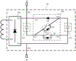
继续参见图1,在上述各实施例的基础上,可选地,整流滤波模块30的输出端包括第一输出端301和第二输出端302;滤波单元包括第一滤波单元311和第二滤波单元312,第一滤波单元311的第一端与整流滤波模块30的第一输出端301电连接,第二滤波单元312的第二端与整流滤波模块30的第二输出端302电连接。整流滤波模块30还包括:第一整流单元320和第一滤波切换单元330,第一整流单元320的第一输入端321作为整流滤波模块30的第一输入端,第一整流单元320的第二输入端322作为整流滤波模块30的第二输入端,第一整流单元320的第一输出端323与整流滤波模块30的第一输出端301电连接,第一整流单元320的第二输出端324与整流滤波模块30的第二输出端302电连接;第一滤波切换单元330包括第一端331、第二端332、第三端333和第四端334;第一滤波切换单元330的第一端331与整流滤波模块30的第一输出端301电连接,第一滤波切换单元330的第二端332与第一滤波单元311的第二端电连接,第一滤波切换单元330的第三端333与第二滤波单元312的第一端电连接,第一滤波切换单元330的第四端334与整流滤波模块30的第二输出端302电连接;第一滤波切换单元330用于在整流滤波模块30的输出端电压为第一电压时,设定第一滤波单元311和第二滤波单元312串联,在整流滤波模块30的输出端电压为第二电压时,设定第一滤波单元311和第二滤波单元312并联。Continuing to refer to FIG. 1 , on the basis of the foregoing embodiments, optionally, the output end of the rectification and
其中,第一整流单元320为可以将其输入端输入的交流电转换为直流电,该第一整流单元320可以为全桥整流电路、倍压整流电路或科克罗夫特-沃尔顿(Cockcroft-Walton)电路,科克罗夫特-沃尔顿电路简称CW电路。示例性地,该整流滤波模块30的工作过程为,参见图2,在高压工作模态,第一滤波切换单元330的第一端331和第三端333断开,第二端332和第四端334断开,第一端331和第四端334导通,以使第一滤波单元311和第二滤波单元312串联;串联后第一滤波单元311和第二滤波单元312两端的总电压为V_k_h,变压器的二次侧绕组输出的电压平均值为U_s_h。参见图3,在低压工作模态,第一滤波切换单元330的第一端331和第三端333导通,第二端332和第四端334导通,第一端331和第四端334断开,以使第一滤波单元311和第二滤波单元312并联;并联后第一滤波单元311和第二滤波单元312两端的电压均为V_k_l,变压器的二次侧绕组输出的电压平均值为U_s_l,且V_k_h=2V_k_l,U_s_h=2U_s_l。假设高压工作模态和低压工作模态的切换时间趋于0,则切换前后整流滤波模块30的输出电压满足V_k_h=2V_k_l,如果考虑到切换过程中电容能量的损失,则需要通过逆变器补充部分能量后实现V_k_h=2V_k_l。Wherein, the
其中,在从低压工作模态向高压工作模态切换的过程中,逆变器需要将变压器的二次侧绕组电压从U_s_l抬升到U_s_h,相比于现有技术,逆变器只需要提供维持负载电流所需能量,不需要向滤波单元提供大量的充电能量,从而使逆变器的短时高电流应力大幅降低。在从高压工作模态向低压工作模态切换的过程中,逆变器需要将变压器的二次侧绕组电压从U_s_h降低到U_s_l,滤波单元的降压过程无需伴随能量释放,所以即使是小电流负载下也可以实现快速降压。Among them, in the process of switching from the low-voltage working mode to the high-voltage working mode, the inverter needs to raise the voltage of the secondary winding of the transformer from U_s_1 to U_s_h. Compared with the prior art, the inverter only needs to provide maintenance The energy required by the load current does not need to provide a large amount of charging energy to the filter unit, so that the short-term high current stress of the inverter is greatly reduced. In the process of switching from the high-voltage working mode to the low-voltage working mode, the inverter needs to reduce the voltage of the secondary winding of the transformer from U_s_h to U_s_l, and the step-down process of the filter unit does not need to be accompanied by energy release, so even a small current Fast step-down can also be achieved under load.
图4为本发明实施例提供的另一种电压切换电路的电路结构示意图。在上述各实施例的基础上,本发明实施例提供了一种第一滤波切换单元330的具体电路结构。参见图4,可选地,第一滤波切换单元330包括:第一晶体管S1、第二晶体管S2和第三晶体管S3。第一晶体管S1的第一端与第一滤波切换单元330的第一端电连接,第一晶体管S1的第二端与第一滤波切换单元330的第三端电连接;第二晶体管S2的第一端与第一滤波切换单元330的第三端电连接,第二晶体管S2的第二端与第一滤波切换单元330的第二端电连接;第三晶体管S3的第一端与第一滤波切换单元330的第二端电连接,第三晶体管S3的第二端与第一滤波切换单元330的第四端电连接;其中,晶体管的体二极管的阴极作为晶体管的第一端;晶体管的体二极管的阳极作为晶体管的第二端。FIG. 4 is a schematic diagram of a circuit structure of another voltage switching circuit provided by an embodiment of the present invention. On the basis of the foregoing embodiments, the embodiments of the present invention provide a specific circuit structure of the first
其中,第一晶体管S1、第二晶体管S2和第三晶体管S3为具有开关功能的晶体管,例如可以是,金属-氧化物半导体场效应晶体管(Metal-Oxide-Semiconductor Field-EffectTransistor,MOSFET)或绝缘栅双极型晶体管(Insulated Gate Bipolar Transistor,IGBT)。示例性地,该第一滤波切换单元330的工作原理为,在高压工作模态,控制第一晶体管S1和第三晶体管S3均断开,控制第二晶体管S2导通,以使第一滤波单元311和第二滤波单元312串联;在低压工作模态,控制第一晶体管S1和第三晶体管S3均导通,控制第二晶体管S2断开,以使第一滤波单元311和第二滤波单元312并联。本发明实施例通过开关器件对第一滤波切换单元330的拓扑进行改变,电路结构简单,进一步降低了制造成本。Wherein, the first transistor S1, the second transistor S2 and the third transistor S3 are transistors with switching functions, for example, a metal-oxide-semiconductor field-effect transistor (Metal-Oxide-Semiconductor Field-EffectTransistor, MOSFET) or an insulated gate Bipolar transistor (Insulated Gate Bipolar Transistor, IGBT). Exemplarily, the working principle of the first
图5为本发明实施例提供的又一种电压切换电路的电路结构示意图。在上述各实施例的基础上,本发明实施例提供了另一种第一滤波切换单元330的具体电路结构。参见图5,可选地,第一滤波切换单元330包括:第一二极管D1、第四晶体管S4和第五晶体管S5。第一二极管D1的阴极与第一滤波切换单元330的第一端电连接,第一二极管D1的阳极与第一滤波切换单元330的第三端电连接;第四晶体管S4的第一端与第一滤波切换单元330的第三端电连接,第四晶体管S4的第二端与第一滤波切换单元330的第二端电连接;第五晶体管S5的第一端与第一滤波切换单元330的第二端电连接,第五晶体管S5的第二端与第一滤波切换单元330的第四端电连接;其中,晶体管的体二极管的阴极作为晶体管的第一端;晶体管的体二极管的阳极作为晶体管的第二端。FIG. 5 is a schematic diagram of a circuit structure of another voltage switching circuit provided by an embodiment of the present invention. On the basis of the foregoing embodiments, the embodiments of the present invention provide another specific circuit structure of the first
示例性地,该第一滤波切换单元330的工作原理为,参见图2,在高压工作模态,控制第五晶体管S5断开,控制第四晶体管S4导通,由于第一二极管D1反向截止,第一滤波单元311和第二滤波单元312串联连接于整流滤波模块30的第一输出端301和第二输出端302之间;在低压工作模态,参见图6,控制第五晶体管S5导通,控制第四晶体管S4断开,由于第一二极管D1反向截止,仅有第一滤波单元311串联于整流滤波模块30的第一输出端301和第二输出端302之间。本发明实施例电路结构简单,进一步降低了制造成本。Exemplarily, the working principle of the first
需要说明的是,图4所示的实施方式在高压工作模态,滤波单元的电容值为0.5C,在低压工作模态,滤波单元的电容值为2C;图5所示的实施方式在高压工作模态,滤波单元的电容值为0.5C,在低压工作模态,滤波单元的电容值为C;因此,图5所示的实施方式的滤波单元的电容值变化幅度更小。其中,图4所示的实施方式可以确保第一滤波单元311和第二滤波单元312均连接于电压切换电路中,因此,第一滤波单元311和第二滤波单元312上的电压(电荷量)得以保持。然而图5所示的实施方式在低压工作模态下,第二滤波单元312不接在电压切换电路中,会使得第二滤波单元312两端的电压下降。在从低压工作模态向高压工作模态的切换过程中,图5所示的实施方式需要重新给第二滤波单元312充电,引起电流的波动。若将本发明实施例提供的电压切换电路应用于双能CT中,因为CT单视图时间很短,约为数百μs,即使采用图5所示的实施方式,在低压工作模态下,第二滤波单元312上的电压下降的很小,因此不会影响双能CT的正常工作。It should be noted that in the embodiment shown in FIG. 4 , the capacitance value of the filter unit is 0.5C in the high-voltage operating mode, and the capacitance value of the filter unit is 2C in the low-voltage operating mode; the embodiment shown in FIG. 5 is in the high-voltage operating mode. In the working mode, the capacitance value of the filter unit is 0.5C, and in the low-voltage working mode, the capacitance value of the filter unit is C; therefore, the capacitance value of the filter unit in the embodiment shown in FIG. 5 changes less. The embodiment shown in FIG. 4 can ensure that both the
还需要说明的是,在前述各实施例中,高压工作模态输出的电压是低压工作模态输出电压的两倍,并非对本发明的限定,在其他实施例中,还可以设置高压工作模态和低压工作模态为任意值的输出电压,在实际应用中可以根据需要进行限定。It should also be noted that, in the foregoing embodiments, the output voltage of the high-voltage working mode is twice the output voltage of the low-voltage working mode, which is not a limitation of the present invention. In other embodiments, the high-voltage working mode can also be set. And the low-voltage working mode is an output voltage of any value, which can be limited according to needs in practical applications.
图7为本发明实施例提供的又一种电压切换电路的电路结构示意图。参见图7,在上述各实施例的基础上,可选地,电压切换电路包括:第一整流滤波模块31、第一逆变器41、第一变压器51、第二逆变器42、第二变压器52和第二整流滤波模块32。第一变压器51的一次侧绕组与第一逆变器41的输出端电连接;第二变压器52的一次侧绕组与第二逆变器42的输出端电连接。整流滤波模块为第一整流滤波模块31,第一整流滤波模块31的输入端与第一变压器51的二次侧绕组电连接;第一整流滤波模块31的第一输出端311与第一切换输出端10电连接;第二整流滤波模块32的输入端与第二变压器52的二次侧绕组电连接;第二整流滤波模块32的第一输出端321与第一整流滤波模块31的第二输出端312电连接;第二整流滤波模块32的第二输出端322与第二切换输出端20电连接。FIG. 7 is a schematic diagram of a circuit structure of another voltage switching circuit provided by an embodiment of the present invention. Referring to FIG. 7 , on the basis of the foregoing embodiments, optionally, the voltage switching circuit includes: a first rectification and
其中,第一逆变器41向第一变压器51提供第一交流电压,第一变压器51向第一整流滤波模块31提供第二交流电压,第一逆变器41、第一变压器51和第一整流滤波模块31构成了第一路功率回路。第二逆变器42向第二变压器52提供第三交流电压,第二变压器52向第二整流滤波模块32提供第四交流电压,第二逆变器42、第二变压器52和第二整流滤波模块32构成了第二路功率回路。第一整流滤波模块31为本发明实施例提供的如图1-图6所示的任意一种整流滤波模块,第二整流滤波模块32可以为本发明实施例提供的任意一种整流滤波模块,也可以为现有技术中的任意一种具有整流滤波功能的模块。第一整流滤波模块31和第二整流滤波模块32串联连接,第一切换输出端10和第二切换输出端20之间的电压为第一整流滤波模块31和第二整流滤波模块32输出电压的和。本发明实施例针对第一整流滤波模块31和第二整流滤波模块32分别设置两路功率回路,避免了在不同工作模态的相互干扰。本发明实施例通过设置两路功率回路分别向第一整流滤波模块31和第二整流滤波模块32提供交流电压,通过第一整流滤波模块31和第二整流滤波模块32输出的两电压值的叠加可以获得两个电压等级为任意值的输出电压。The
图8为本发明实施例提供的一种电压切换电路输出电压的波形示意图。参见图8,在上述各实施例的基础上,可选地,第一切换输出端10和第二切换输出端20输出电压为第一电压kV_h或第二电压kV_l;第一整流滤波模块31的输出电压为kV_h-kV_l或2(kV_h-kV_l);第二整流滤波模块32的输出电压为2kV_l-kV_h。示例性地,图8中的波形101为第一整流滤波模块31输出电压的波形,第一整流滤波模块31的输出电压在kV_h-kV_l和2(kV_h-kV_l)之间切换;波形102为第二整流滤波模块32输出电压的波形,第二整流滤波模块32的输出电压为2kV_l-kV_h;波形103为第一切换输出端10和第二切换输出端20输出电压的波形,第一切换输出端10和第二切换输出端20的输出电压在kV_l和kV_h之间切换。第二整流滤波模块32的输出电压为恒定的值,第一整流滤波模块31输出kV_h-kV_l时,第一切换输出端10和第二切换输出端20输出电压为第一电压kV_l;第一整流滤波模块31输出2(kV_h-kV_l)时,第一切换输出端10和第二切换输出端20输出电压为第一电压kV_h。本发明实施例这样设置实现了两个电压等级为任意值的输出电压。FIG. 8 is a schematic waveform diagram of an output voltage of a voltage switching circuit according to an embodiment of the present invention. Referring to FIG. 8 , on the basis of the above embodiments, optionally, the output voltage of the first
需要说明的是,以上实施例中,整流单元的拓扑结构在电压切换过程中没有发生变化,而滤波切换单元的拓扑发生变化,以使滤波单元的电容值发生变化,其并非对本发明的限定,在其他实施例中,还可以设置整流单元的拓扑结构也发生变化,在实际应用中可以根据需要进行设置。It should be noted that, in the above embodiment, the topology of the rectifier unit does not change during the voltage switching process, but the topology of the filter switching unit changes, so that the capacitance value of the filter unit changes, which is not a limitation of the present invention. In other embodiments, the topology structure of the rectifier unit can also be set to change, which can be set as required in practical applications.
图9为本发明实施例提供的又一种电压切换电路的电路结构示意图。参见图9,在上述各实施例的基础上,可选地,整流滤波模块30的输出端包括第一输出端301和第二输出端302;滤波单元包括第三滤波单元313和第四滤波单元314,第三滤波单元313的第一端与整流滤波模块30的第一输出端301电连接,第四滤波单元314的第二端与整流滤波模块30的第二输出端302电连接。整流滤波模块30还包括:第二整流单元340和第二滤波切换单元350;第二整流单元340的第一输入端341作为整流滤波模块30的第一输入端,第二整流单元340的第二输入端342作为整流滤波模块30的第二输入端,第二整流单元340的第一输出端343与整流滤波模块30的第一输出端301电连接,第二整流单元340的第二输出端344与整流滤波模块30的第二输出端302电连接;第二整流单元340用于在整流滤波模块30的输出端电压为第一电压时,设定第二整流单元340为第一拓扑结构,在整流滤波模块30的输出端电压为第二电压时,设定第二整流单元340为第二拓扑结构;第二滤波切换单元350包括第一端351、第二端352、第三端353、第四端354和第五端355;第二滤波切换单元350的第一端351与整流滤波模块30的第一输出端301电连接,第二滤波切换单元350的第二端352与第三滤波单元313的第二端352电连接,第二滤波切换单元350的第三端353与整流滤波模块30的第二输入端342电连接,第二滤波切换单元350的第四端354与第四滤波单元314的第一端351电连接,第二滤波切换单元350的第五端355与整流滤波模块30的第二输出端302电连接;第二滤波切换单元350用于在整流滤波模块30的输出端电压为第一电压时,设定滤波单元的电容值为第三滤波单元313的电容值或第四滤波单元314的电容值,在整流滤波模块30的输出端电压为第二电压时,设定第三滤波单元313和第四滤波单元314并联。FIG. 9 is a schematic diagram of a circuit structure of another voltage switching circuit provided by an embodiment of the present invention. Referring to FIG. 9 , on the basis of the foregoing embodiments, optionally, the output end of the rectification and
其中,第二整流单元340的拓扑结构可以是全桥整流拓扑、倍压整流拓扑或CW整流拓扑。示例性地,第一拓扑结构为倍压整流拓扑,第二拓扑结构为全桥整流拓扑。该整流滤波模块30的工作过程为,参见图10,在高压工作模态,第二整流单元340的拓扑结构为倍压整流拓扑,第二滤波切换单元350的第二端352和第三端353导通,第三端353和第四端354导通,以使第一滤波单元311和第二滤波单元312串联,串联后的第一滤波单元311和第二滤波单元312两端的总电压为V_k_h,变压器的二次侧绕组输出的电压平均值为U_s_h;参见图11,在低压工作模态,第二整流单元340的拓扑结构为全桥整流拓扑,第二滤波切换单元350的第一端351和第四端354导通,第二端352和第五端355导通,以使第一滤波单元311和第二滤波单元312并联,并联后第一滤波单元311和第二滤波单元312两端的电压均为V_k_l;变压器的二次侧绕组输出的电压平均值为U_s_l,V_k_h=2V_k_l,U_s_h=U_s_l。The topology of the
由此可见,无论在低压工作模态还是高压工作模态,变压器的二次侧绕组电压不变。相比于现有技术,在从低压工作模态向高压工作模态切换的过程中,逆变器不需要向滤波单元提供大量的充电能量,从而使逆变器的短时高电流应力大幅降低。在从高压工作模态向低压工作模态切换的过程中,滤波单元的降压过程无需伴随能量释放,所以即使是小电流负载下也可以实现快速降压。It can be seen that no matter in the low-voltage working mode or the high-voltage working mode, the voltage of the secondary winding of the transformer remains unchanged. Compared with the prior art, in the process of switching from the low-voltage working mode to the high-voltage working mode, the inverter does not need to provide a large amount of charging energy to the filter unit, so that the short-term high current stress of the inverter is greatly reduced. . In the process of switching from the high-voltage working mode to the low-voltage working mode, the step-down process of the filter unit does not need to be accompanied by energy release, so even under a small current load, a rapid step-down can be achieved.
图12为本发明实施例提供的又一种电压切换电路的电路结构示意图。参见图11,在上述各实施例的基础上,可选地,第二整流单元340包括:第二二极管D2、第三二极管D3、第四二极管D4、第六晶体管S6、第七晶体管S7和第五二极管D5。第二二极管D2的阳极与第二整流单元340的第一输入端341电连接,第二二极管D2的阴极与第二整流单元340的第一输出端343电连接;第三二极管D3的阳极与第二整流单元340的第二输出端344电连接,第三二极管D3的阴极与第二整流单元340的第一输入端341电连接;第四二极管D4的阴极与第二整流单元340的第一输出端343电连接;第六晶体管S6的第一端与第二整流单元340的第二输入端342电连接,第六晶体管S6的第二端与第四二极管D4的阳极电连接;第七晶体管S7的第二端与第二整流单元340的第二输入端342电连接;第五二极管D5的阳极与第二整流单元340的第二输出端344电连接,第五二极管D5的阴极与第七晶体管S7的第一端电连接;其中,晶体管的体二极管的阴极作为晶体管的第一端;晶体管的体二极管的阳极作为晶体管的第二端。FIG. 12 is a schematic diagram of a circuit structure of another voltage switching circuit provided by an embodiment of the present invention. Referring to FIG. 11, on the basis of the foregoing embodiments, optionally, the
其中,第六晶体管S6和第七晶体管S7为具有开关功能的晶体管,例如可以是,MOSFET或IGBT。示例性地,该第二整流单元340的工作原理为,在高压工作模态,控制第六晶体管S6和第七晶体管S7均断开,以使第二整流单元340为第一拓扑结构;在低压工作模态,控制第六晶体管S6和第七晶体管S7均导通,以使第二整流单元340为第二拓扑结构。本发明实施例通过开关器件对第二整流单元340的拓扑结构进行变换,电路结构简单,成本低。The sixth transistor S6 and the seventh transistor S7 are transistors with switching functions, for example, MOSFETs or IGBTs. Exemplarily, the working principle of the
继续参见图12,在上述各实施例的基础上,可选地,第二滤波切换单元350包括:第八晶体管S8、第九晶体管S9、第十晶体管S10和第十一晶体管S11。第八晶体管S8的第一端与第二滤波切换单元350的第三端353电连接,第八晶体管S8的第二端与第二滤波切换单元350的第二端352电连接;第九晶体管S9的第一端与第二滤波切换单元350的第四端354电连接,第九晶体管S9的第二端与第二滤波切换单元350的第三端353电连接;第十晶体管S10的第一端与第二滤波切换单元350的第一端351电连接,第十晶体管S10的第二端与第二滤波切换单元350的第四端354电连接;第十一晶体管S11的第一端与第二滤波切换单元350的第二端352电连接,第十一晶体管S11的第二端与第二滤波切换单元350的第五端355电连接;其中,晶体管的体二极管的阴极作为晶体管的第一端;晶体管的体二极管的阳极作为晶体管的第二端。Continuing to refer to FIG. 12 , on the basis of the foregoing embodiments, optionally, the second
其中,第八晶体管S8、第九晶体管S9、第十晶体管S10和第十一晶体管S11为具有开关功能的晶体管,例如可以是,MOSFET或IGBT。示例性地,该第二整流单元340的工作原理为,在高压工作模态,控制第八晶体管S8和第九晶体管S9均导通,控制第十晶体管S10和第十一晶体管S11均断开,以使第一滤波单元311和第二滤波单元312串联;在低压工作模态,控制第八晶体管S8和第九晶体管S9均断开,控制第十晶体管S10和第十一晶体管S11均导通。本发明实施例通过开关器件对第二滤波切换单元350的拓扑结构进行变换,电路结构简单,进一步降低了制造成本。The eighth transistor S8 , the ninth transistor S9 , the tenth transistor S10 and the eleventh transistor S11 are transistors with switching functions, for example, MOSFETs or IGBTs. Exemplarily, the working principle of the
图13为本发明实施例提供的又一种电压切换电路的电路结构示意图。参见图13,在上述各实施例的基础上,可选地,电压切换电路还包括:第三逆变器43、第三变压器53、第三整流滤波模块33和第四整流滤波模块34,第三变压器53的一次侧绕组与第三逆变器43的输出端电连接;第三变压器53包括第一二次侧绕组和第二二次侧绕组。第三整流滤波模块33的第一输入端与第一二次侧绕组的第一端531电连接;第三整流滤波模块33的第二输入端与第一二次侧绕组的第二端532电连接;第三整流滤波模块33的第一输出端331与第一切换输出端10电连接;第四整流滤波模块34的第一输入端与第二二次侧绕组的第一端533电连接;第四整流滤波模块34的第二输入端与第二二次侧绕组的第二端534电连接;第四整流滤波模块34的第一输出端341与第三整流滤波模块33的第二输出端332电连接;第四整流滤波模块34的第二输出端342与第二切换输出端20电连接。FIG. 13 is a schematic diagram of a circuit structure of another voltage switching circuit provided by an embodiment of the present invention. Referring to FIG. 13 , on the basis of the foregoing embodiments, optionally, the voltage switching circuit further includes: a
其中,第三逆变器43向第三变压器53提供第五交流电压,第三变压器53向第三整流滤波模块33提供第六交流电压,第三变压器53向第四整流滤波模块34提供第七交流电压,第六交流电压和第七交流电压的取值由变压器的变比决定。第三整流滤波模块33为本发明实施例提供的如图9-图12所示的任意一种整流滤波模块,第四整流滤波模块34可以为本发明实施例提供的任意一种整流滤波模块,也可以为现有技术中任意一种具有整流滤波功能的模块。第三整流滤波模块33和第四整流滤波模块34串联连接,第一切换输出端10和第二切换输出端20之间的电压为第三整流滤波模块33和第四整流滤波模块34输出电压的和。本发明实施例通过设置第三整流滤波模块33和第四整流滤波模块34分别输出两种电压值,通过两电压值的叠加可以获得两个电压等级为任意值的输出电压。The
在上述各实施例的基础上,可选地,第一切换输出端10和第二切换输出端20输出电压为第一电压kV_h或第二电压kV_l;第三整流滤波模块33的输出电压为kV_h-kV_l或2(kV_h-kV_l);第四整流滤波模块34的输出电压为2kV_l-kV_h。其中,第四整流滤波模块34的输出电压为恒定的值,第三整流滤波模块33输出kV_h-kV_l时,第一切换输出端10和第二切换输出端20输出电压为第一电压kV_l;第三整流滤波模块33输出2(kV_h-kV_l)时,第一切换输出端10和第二切换输出端20输出电压为第一电压kV_h。本发明实施例这样设置实现了两个电压等级为任意值的输出电压。On the basis of the above embodiments, optionally, the output voltage of the first
需要说明的是,由于本发明实施例提供的第三整流滤波模块33在输出两个电压等级时,其前端二次侧绕组输出的电压保持不变,第四整流滤波模块34的前端二次侧绕组输出的电压保持不变,因此,第三整流滤波模块33和第四整流滤波模块34可以连接在第三变压器53的不同绕组上。与设置第三整流滤波模块33和第四整流滤波模块34分别连接不同的逆变器和变压器相比,本发明实施例进一步降低了电压切换电路的制作成本。It should be noted that, since the voltage output by the front-end secondary side winding of the third rectifier and
图14为本发明实施例提供的又一种电压切换电路的电路结构示意图。参见图14,在上述各实施例的基础上,可选地,整流滤波模块30的数量为N个;其中,第一个整流滤波模块30的第一输出端301与第一切换输出端10电连接,第i个整流滤波模块30的第四端与第i+1个整流滤波模块30的第一输出端301电连接,第N个整流滤波模块30的第四端与第二切换输出端20电连接;N≥1,1≤i<N。FIG. 14 is a schematic diagram of a circuit structure of another voltage switching circuit provided by an embodiment of the present invention. Referring to FIG. 14 , on the basis of the above-mentioned embodiments, optionally, the number of rectification and
本发明实施例提供的整流滤波模块30的数量为至少一个,若整流滤波模块30的数量为一个,整流滤波模块30的输出端即为电压切换电路的输出端;若整流滤波模块30的数量为多个(两个及两个以上),多个整流滤波模块30串联连接,具体连接方式为,第一个整流滤波模块30的第一输出端与第一切换输出端10电连接,第一个整流滤波模块30的第二输出端与第二个整流滤波模块30的第一输出端电连接,以此类推,最后一个整流滤波模块30的第二输出端与第二切换输出端20电连接。在实际应用中可以根据需要设置串联连接的整流滤波模块30的具体数量。The number of the rectifier and filter
在上述各实施例的基础上,可选地,电压切换电路还包括:控制系统,控制系统与电压切换电路连接,用于控制所述电压切换电路的电压输出端的电压。其中,电压切换电路例如可以包括逆变器、整流单元、滤波切换单元等电路结构。在这些电路结构中,例如可以包括多种晶体管,通过控制系统可以对这些晶体管的控制端进行控制,以控制这些晶体管的开通和关断,从而切换电路的拓扑结构,进而实现电压等级的切换。On the basis of the above embodiments, optionally, the voltage switching circuit further includes: a control system, the control system is connected to the voltage switching circuit, and is used for controlling the voltage of the voltage output terminal of the voltage switching circuit. The voltage switching circuit may include, for example, circuit structures such as an inverter, a rectifier unit, and a filter switching unit. In these circuit structures, for example, a variety of transistors may be included, and the control terminals of these transistors can be controlled by the control system to control the turn-on and turn-off of these transistors, thereby switching the topology of the circuit, thereby realizing the switching of voltage levels.
本发明实施例还提供了一种双能CT。图15为本发明实施例提供的一种双能CT的电路结构示意图。参见图15,该双能CT包括:本发明任意实施例所提供的电压切换电路1和球管2;球管2的供电端与电压切换电路的电压输出端电连接,高压发生器用于向球管供电。其中,电压切换电路1的电压输出端包括第一切换输出端10和第二切换输出端20,第一切换输出端10和第二切换输出端20之间的电压差为电压切换电路1的输出电压。The embodiment of the present invention also provides a dual-energy CT. FIG. 15 is a schematic diagram of a circuit structure of a dual-energy CT provided by an embodiment of the present invention. Referring to FIG. 15 , the dual-energy CT includes: the
本发明实施例通过切换电压切换电路1中整流滤波模块的滤波单元的电容值,使得滤波单元的电容值被设定为第一电容值,整流滤波模块的输出端电压为第一电压;滤波单元的电容值被设定为第二电容值,整流滤波模块的输出端电压为第二电压;且滤波单元的电压和电容值呈负相关,从而有利于在输出两个电压等级的切换过程中,使得滤波单元的电荷量几乎不变,即有利于减小滤波单元的充放电时间。与现有技术相比,本发明实施例在输出两个电压等级切换的过程中,滤波单元的电荷量变化较小,因而无需对滤波单元进行长时间的充放电,一方面,提升了电压切换速度,且电压切换速度不受负载电流变化的影响,另一方面,无需采用电流应力较好的逆变器。因此,本发明实施例实现了提升电压切换速度、降低成本和适用负载电流范围大的效果。In the embodiment of the present invention, by switching the capacitance value of the filter unit of the rectification filter module in the
注意,上述仅为本发明的较佳实施例及所运用技术原理。本领域技术人员会理解,本发明不限于这里所述的特定实施例,对本领域技术人员来说能够进行各种明显的变化、重新调整和替代而不会脱离本发明的保护范围。因此,虽然通过以上实施例对本发明进行了较为详细的说明,但是本发明不仅仅限于以上实施例,在不脱离本发明构思的情况下,还可以包括更多其他等效实施例,而本发明的范围由所附的权利要求范围决定。Note that the above are only preferred embodiments of the present invention and applied technical principles. Those skilled in the art will understand that the present invention is not limited to the specific embodiments described herein, and various obvious changes, readjustments and substitutions can be made by those skilled in the art without departing from the protection scope of the present invention. Therefore, although the present invention has been described in detail through the above embodiments, the present invention is not limited to the above embodiments, and can also include more other equivalent embodiments without departing from the concept of the present invention. The scope is determined by the scope of the appended claims.
Claims (18)
Priority Applications (1)
| Application Number | Priority Date | Filing Date | Title |
|---|---|---|---|
| CN201910193303.2A CN109787494B (en) | 2019-03-14 | 2019-03-14 | A voltage switching circuit and dual energy CT |
Applications Claiming Priority (1)
| Application Number | Priority Date | Filing Date | Title |
|---|---|---|---|
| CN201910193303.2A CN109787494B (en) | 2019-03-14 | 2019-03-14 | A voltage switching circuit and dual energy CT |
Publications (2)
| Publication Number | Publication Date |
|---|---|
| CN109787494A CN109787494A (en) | 2019-05-21 |
| CN109787494B true CN109787494B (en) | 2020-12-22 |
Family
ID=66487966
Family Applications (1)
| Application Number | Title | Priority Date | Filing Date |
|---|---|---|---|
| CN201910193303.2A Active CN109787494B (en) | 2019-03-14 | 2019-03-14 | A voltage switching circuit and dual energy CT |
Country Status (1)
| Country | Link |
|---|---|
| CN (1) | CN109787494B (en) |
Families Citing this family (1)
| Publication number | Priority date | Publication date | Assignee | Title |
|---|---|---|---|---|
| CN113271029A (en) * | 2021-05-28 | 2021-08-17 | 青岛大学 | DAB type single-stage bidirectional AC/DC converter with low voltage stress and wide output range |
Citations (3)
| Publication number | Priority date | Publication date | Assignee | Title |
|---|---|---|---|---|
| CN1893243A (en) * | 2005-07-01 | 2007-01-10 | 株式会社三社电机制作所 | Power supply device for electrocladding |
| CN204967638U (en) * | 2015-05-25 | 2016-01-13 | 张家港市华为电子有限公司 | Be fit for automatic switch -over circuit among 220V and 110V electric network source |
| CN208046460U (en) * | 2018-04-11 | 2018-11-02 | 中兴通讯股份有限公司 | A kind of converter |
Family Cites Families (2)
| Publication number | Priority date | Publication date | Assignee | Title |
|---|---|---|---|---|
| CN104753338B (en) * | 2013-12-25 | 2018-03-23 | 台达电子企业管理(上海)有限公司 | Power Electronic Circuit and power model |
| CN103997243A (en) * | 2014-05-28 | 2014-08-20 | 南京理工大学 | Double-end flyback high-frequency isolation type three-level inverter |
-
2019
- 2019-03-14 CN CN201910193303.2A patent/CN109787494B/en active Active
Patent Citations (3)
| Publication number | Priority date | Publication date | Assignee | Title |
|---|---|---|---|---|
| CN1893243A (en) * | 2005-07-01 | 2007-01-10 | 株式会社三社电机制作所 | Power supply device for electrocladding |
| CN204967638U (en) * | 2015-05-25 | 2016-01-13 | 张家港市华为电子有限公司 | Be fit for automatic switch -over circuit among 220V and 110V electric network source |
| CN208046460U (en) * | 2018-04-11 | 2018-11-02 | 中兴通讯股份有限公司 | A kind of converter |
Also Published As
| Publication number | Publication date |
|---|---|
| CN109787494A (en) | 2019-05-21 |
Similar Documents
| Publication | Publication Date | Title |
|---|---|---|
| CN103715897B (en) | Isolated converter and apply its Switching Power Supply | |
| CN108206634B (en) | Insulating synchronous rectification DC/DC converter, controller, adapter and equipment | |
| US20060274887A1 (en) | X-ray high voltage device | |
| US9906169B1 (en) | DC-AC conversion circuit having a first double ended DC pulse stage and a second AC stage | |
| CN107453615B (en) | Modular Multilevel Converters and Power Electronic Transformers | |
| US10361624B2 (en) | Multi-cell power converter with improved start-up routine | |
| US9144146B2 (en) | High voltage driving device for X-ray tube | |
| CN103200755A (en) | Power generation system, X-ray emitter system and power generation system packaging | |
| CN109787494B (en) | A voltage switching circuit and dual energy CT | |
| Park et al. | 60 V-to-35 kV input-parallel output-series DC-DC converter using multi-level class-DE rectifiers | |
| CN102361391A (en) | Power gaining circuit applicable to high-voltage field | |
| CN107482944A (en) | One kind output adjustable all solid state high voltage power supply of pulse multi-parameter | |
| JP4026419B2 (en) | Capacitor charger | |
| KR102724598B1 (en) | Appratus for generating x-ray and method thereof | |
| CN118381290A (en) | Power supply circuit and power conversion device | |
| CN214674929U (en) | Magnetron device and magnetron power supply circuit | |
| CN212086069U (en) | High-voltage circuit for G-M counting tube | |
| CN107231098A (en) | Half/full-bridge pulse voltage superimposer of cascade connection type simplifies isolation charging system and method | |
| JP3922524B2 (en) | Electron tube equipment | |
| CN115734444B (en) | Method and circuit arrangement for operating an X-ray tube and X-ray device | |
| US20220255443A1 (en) | Power conversion apparatus | |
| JP2015008589A (en) | Switching power-supply device | |
| US20200235673A1 (en) | Power supply and power supply unit | |
| JPH11266582A (en) | X-ray high voltage unit | |
| CN214707264U (en) | Charging device |
Legal Events
| Date | Code | Title | Description |
|---|---|---|---|
| PB01 | Publication | ||
| PB01 | Publication | ||
| SE01 | Entry into force of request for substantive examination | ||
| SE01 | Entry into force of request for substantive examination | ||
| CB02 | Change of applicant information | ||
| CB02 | Change of applicant information |
Address after: 201807 Shanghai City, north of the city of Jiading District Road No. 2258 Applicant after: Shanghai Lianying Medical Technology Co., Ltd Address before: 201807 Shanghai City, north of the city of Jiading District Road No. 2258 Applicant before: SHANGHAI UNITED IMAGING HEALTHCARE Co.,Ltd. |
|
| GR01 | Patent grant | ||
| GR01 | Patent grant |