CN109427973B - Capacitor with vertical contacts extending through a conductive layer - Google Patents

Capacitor with vertical contacts extending through a conductive layer Download PDF

Info

Publication number
CN109427973B
CN109427973B CN201810996618.6A CN201810996618A CN109427973B CN 109427973 B CN109427973 B CN 109427973B CN 201810996618 A CN201810996618 A CN 201810996618A CN 109427973 B CN109427973 B CN 109427973B
Authority
CN
China
Prior art keywords
conductive
contact
contacts
dielectric material
dielectric
Prior art date
Legal status (The legal status is an assumption and is not a legal conclusion. Google has not performed a legal analysis and makes no representation as to the accuracy of the status listed.)
Active
Application number
CN201810996618.6A
Other languages
Chinese (zh)
Other versions
CN109427973A (en
Inventor
P·泰萨里欧
汤强
Current Assignee (The listed assignees may be inaccurate. Google has not performed a legal analysis and makes no representation or warranty as to the accuracy of the list.)
Micron Technology Inc
Original Assignee
Micron Technology Inc
Priority date (The priority date is an assumption and is not a legal conclusion. Google has not performed a legal analysis and makes no representation as to the accuracy of the date listed.)
Filing date
Publication date
Application filed by Micron Technology Inc filed Critical Micron Technology Inc
Publication of CN109427973A publication Critical patent/CN109427973A/en
Application granted granted Critical
Publication of CN109427973B publication Critical patent/CN109427973B/en
Active legal-status Critical Current
Anticipated expiration legal-status Critical

Links

Images

Classifications

    • HELECTRICITY
    • H10SEMICONDUCTOR DEVICES; ELECTRIC SOLID-STATE DEVICES NOT OTHERWISE PROVIDED FOR
    • H10DINORGANIC ELECTRIC SEMICONDUCTOR DEVICES
    • H10D1/00Resistors, capacitors or inductors
    • H10D1/60Capacitors
    • H10D1/68Capacitors having no potential barriers
    • HELECTRICITY
    • H10SEMICONDUCTOR DEVICES; ELECTRIC SOLID-STATE DEVICES NOT OTHERWISE PROVIDED FOR
    • H10BELECTRONIC MEMORY DEVICES
    • H10B20/00Read-only memory [ROM] devices
    • H10B20/60Peripheral circuit regions
    • HELECTRICITY
    • H10SEMICONDUCTOR DEVICES; ELECTRIC SOLID-STATE DEVICES NOT OTHERWISE PROVIDED FOR
    • H10BELECTRONIC MEMORY DEVICES
    • H10B41/00Electrically erasable-and-programmable ROM [EEPROM] devices comprising floating gates
    • H10B41/20Electrically erasable-and-programmable ROM [EEPROM] devices comprising floating gates characterised by three-dimensional [3D] arrangements, e.g. with cells on different height levels
    • H10B41/23Electrically erasable-and-programmable ROM [EEPROM] devices comprising floating gates characterised by three-dimensional [3D] arrangements, e.g. with cells on different height levels with source and drain on different levels, e.g. with sloping channels
    • H10B41/27Electrically erasable-and-programmable ROM [EEPROM] devices comprising floating gates characterised by three-dimensional [3D] arrangements, e.g. with cells on different height levels with source and drain on different levels, e.g. with sloping channels the channels comprising vertical portions, e.g. U-shaped channels
    • HELECTRICITY
    • H10SEMICONDUCTOR DEVICES; ELECTRIC SOLID-STATE DEVICES NOT OTHERWISE PROVIDED FOR
    • H10BELECTRONIC MEMORY DEVICES
    • H10B43/00EEPROM devices comprising charge-trapping gate insulators
    • H10B43/20EEPROM devices comprising charge-trapping gate insulators characterised by three-dimensional [3D] arrangements, e.g. with cells on different height levels
    • H10B43/23EEPROM devices comprising charge-trapping gate insulators characterised by three-dimensional [3D] arrangements, e.g. with cells on different height levels with source and drain on different levels, e.g. with sloping channels
    • H10B43/27EEPROM devices comprising charge-trapping gate insulators characterised by three-dimensional [3D] arrangements, e.g. with cells on different height levels with source and drain on different levels, e.g. with sloping channels the channels comprising vertical portions, e.g. U-shaped channels
    • HELECTRICITY
    • H10SEMICONDUCTOR DEVICES; ELECTRIC SOLID-STATE DEVICES NOT OTHERWISE PROVIDED FOR
    • H10BELECTRONIC MEMORY DEVICES
    • H10B63/00Resistance change memory devices, e.g. resistive RAM [ReRAM] devices
    • H10B63/80Arrangements comprising multiple bistable or multi-stable switching components of the same type on a plane parallel to the substrate, e.g. cross-point arrays
    • H10B63/84Arrangements comprising multiple bistable or multi-stable switching components of the same type on a plane parallel to the substrate, e.g. cross-point arrays arranged in a direction perpendicular to the substrate, e.g. 3D cell arrays
    • H10B63/845Arrangements comprising multiple bistable or multi-stable switching components of the same type on a plane parallel to the substrate, e.g. cross-point arrays arranged in a direction perpendicular to the substrate, e.g. 3D cell arrays the switching components being connected to a common vertical conductor
    • HELECTRICITY
    • H10SEMICONDUCTOR DEVICES; ELECTRIC SOLID-STATE DEVICES NOT OTHERWISE PROVIDED FOR
    • H10DINORGANIC ELECTRIC SEMICONDUCTOR DEVICES
    • H10D1/00Resistors, capacitors or inductors
    • H10D1/01Manufacture or treatment
    • H10D1/041Manufacture or treatment of capacitors having no potential barriers
    • H10D1/042Manufacture or treatment of capacitors having no potential barriers using deposition processes to form electrode extensions
    • HELECTRICITY
    • H10SEMICONDUCTOR DEVICES; ELECTRIC SOLID-STATE DEVICES NOT OTHERWISE PROVIDED FOR
    • H10DINORGANIC ELECTRIC SEMICONDUCTOR DEVICES
    • H10D1/00Resistors, capacitors or inductors
    • H10D1/60Capacitors
    • H10D1/68Capacitors having no potential barriers
    • H10D1/692Electrodes
    • H10D1/711Electrodes having non-planar surfaces, e.g. formed by texturisation
    • H10D1/714Electrodes having non-planar surfaces, e.g. formed by texturisation having horizontal extensions
    • HELECTRICITY
    • H10SEMICONDUCTOR DEVICES; ELECTRIC SOLID-STATE DEVICES NOT OTHERWISE PROVIDED FOR
    • H10DINORGANIC ELECTRIC SEMICONDUCTOR DEVICES
    • H10D1/00Resistors, capacitors or inductors
    • H10D1/60Capacitors
    • H10D1/68Capacitors having no potential barriers
    • H10D1/692Electrodes
    • H10D1/711Electrodes having non-planar surfaces, e.g. formed by texturisation
    • H10D1/716Electrodes having non-planar surfaces, e.g. formed by texturisation having vertical extensions
    • HELECTRICITY
    • H10SEMICONDUCTOR DEVICES; ELECTRIC SOLID-STATE DEVICES NOT OTHERWISE PROVIDED FOR
    • H10WGENERIC PACKAGES, INTERCONNECTIONS, CONNECTORS OR OTHER CONSTRUCTIONAL DETAILS OF DEVICES COVERED BY CLASS H10
    • H10W20/00Interconnections in chips, wafers or substrates
    • H10W20/01Manufacture or treatment
    • H10W20/031Manufacture or treatment of conductive parts of the interconnections
    • H10W20/0698Local interconnections
    • HELECTRICITY
    • H10SEMICONDUCTOR DEVICES; ELECTRIC SOLID-STATE DEVICES NOT OTHERWISE PROVIDED FOR
    • H10WGENERIC PACKAGES, INTERCONNECTIONS, CONNECTORS OR OTHER CONSTRUCTIONAL DETAILS OF DEVICES COVERED BY CLASS H10
    • H10W20/00Interconnections in chips, wafers or substrates
    • H10W20/20Interconnections within wafers or substrates, e.g. through-silicon vias [TSV]
    • HELECTRICITY
    • H10SEMICONDUCTOR DEVICES; ELECTRIC SOLID-STATE DEVICES NOT OTHERWISE PROVIDED FOR
    • H10WGENERIC PACKAGES, INTERCONNECTIONS, CONNECTORS OR OTHER CONSTRUCTIONAL DETAILS OF DEVICES COVERED BY CLASS H10
    • H10W20/00Interconnections in chips, wafers or substrates
    • H10W20/40Interconnections external to wafers or substrates, e.g. back-end-of-line [BEOL] metallisations or vias connecting to gate electrodes
    • H10W20/495Capacitive arrangements or effects of, or between wiring layers

Landscapes

  • Semiconductor Integrated Circuits (AREA)
  • Engineering & Computer Science (AREA)
  • Power Engineering (AREA)

Abstract

Some embodiments include apparatuses and methods of forming the same. One of the apparatuses includes conductive material located in different levels of the apparatus, dielectric material located in different levels of the apparatus, a first conductive contact, and a second conductive contact. One of the conductive materials is between two of the dielectric materials. One of the dielectric materials is between two of the conductive materials. The first conductive contact has a length extending through the conductive material and the dielectric material in a direction perpendicular to the level of the apparatus. The first conductive contact is electrically separated from the conductive material. The second conductive contact contacts a set of the conductive materials.

Description

具有延伸穿过导电层的竖直触点的电容器Capacitors with vertical contacts extending through conductive layers

技术领域technical field

本申请是关于电容器,且具体来说关于具有延伸穿过导电层的竖直触点的电容器。This application relates to capacitors, and in particular to capacitors having vertical contacts extending through conductive layers.

背景技术Background technique

电容器广泛用于电源电路和计算机中的其它电路、手机和许多其它电子物品中。电容器具有许多不同物理结构。电容器的结构可影响其大小和效率。如下文更详细呈现,本文中所描述的电容器包含可克服一些习知电容器所面对的挑战的结构。Capacitors are widely used in power circuits and other circuits in computers, cell phones and many other electronic items. Capacitors have many different physical structures. The structure of a capacitor can affect its size and efficiency. As presented in more detail below, the capacitors described herein include structures that can overcome some of the challenges faced by conventional capacitors.

发明内容Contents of the invention

本申请的第一方面是关于一种设备,其包括:导电材料,其位于设备的不同层级中;电介质材料,其位于设备的不同层级中,导电材料中的一种在电介质材料中的两种之间,且电介质材料中的一种在导电材料中的两种之间;第一导电触点,其具有在垂直于设备的层级的方向上延伸穿过导电材料和电介质材料的长度,且第一导电触点与导电材料电分离;和第二导电触点,其接触导电材料中的一组导电材料。The first aspect of the present application relates to a device, which includes: conductive materials, which are located in different layers of the device; dielectric materials, which are located in different layers of the device, one of the conductive materials is in two of the dielectric materials and one of the dielectric materials is between two of the conductive materials; a first conductive contact has a length extending through the conductive material and the dielectric material in a direction perpendicular to the level of the device, and the second a conductive contact electrically separated from the conductive material; and a second conductive contact contacting a set of the conductive materials.

本申请的第二方面是关于一种设备,其包括:多个竖直隔开的导电材料层,其在衬底上方延伸;多个竖直隔开的电介质材料层,其与多个导电材料层交错;电容器,其包含:第一导电柱结构,其形成电容器的第一节点,第一导电柱结构竖直地延伸穿过竖直隔开的导电材料层中的至少两个;电容器电介质,其使第一导电柱结构与至少两个竖直隔开的导电材料层电分离,第一导电柱结构延伸穿过至少两个竖直隔开的导电材料层;第二导电柱,其形成电容器的第二节点,第二导电柱竖直地延伸穿过且电耦合到至少两个竖直隔开的导电材料层。A second aspect of the present application is directed to an apparatus comprising: a plurality of vertically spaced layers of conductive material extending over a substrate; a plurality of vertically spaced layers of dielectric material in contact with the plurality of conductive material layer interleaving; a capacitor comprising: a first conductive post structure forming a first node of the capacitor, the first conductive post structure extending vertically through at least two of the vertically spaced apart layers of conductive material; a capacitor dielectric, which electrically separates a first conductive post structure extending through at least two vertically spaced layers of conductive material from at least two vertically spaced layers of conductive material; a second conductive post which forms a capacitor The second node of the second conductive pillar vertically extends through and is electrically coupled to at least two vertically separated conductive material layers.

本申请之第三方面是关于一种设备,其包括:导电材料,其位于设备的不同层级中;电介质材料,其位于设备的不同层级中,导电材料中的一种在电介质材料中的两种之间,且电介质材料中的一种在导电材料中的两种之间;第一导电触点,第一导电触点中的每一个具有在垂直于设备的层级的方向上延伸穿过导电材料和电介质材料的长度,第一导电触点中的每一个通过额外的电介质材料与导电材料分离;第二导电触点,第二导电触点中的每一个具有在垂直于设备的层级的方向上延伸穿过导电材料和电介质材料的长度,第二导电触点中的每一个接触一组导电材料;第一导电区,其接触第一导电触点;和第二导电区,其接触第二导电触点。The third aspect of the present application relates to a device, which includes: conductive materials, which are located in different layers of the device; dielectric materials, which are located in different layers of the device, one of the conductive materials is in two of the dielectric materials between, and one of the dielectric materials is between two of the conductive materials; a first conductive contact, each of which has a direction extending through the conductive material in a direction perpendicular to the level of the device and the length of the dielectric material, each of the first conductive contacts is separated from the conductive material by additional dielectric material; the second conductive contacts, each of the second conductive contacts have a direction perpendicular to the level of the device Extending through the length of the conductive material and the dielectric material, each of the second conductive contacts contacts a set of conductive material; a first conductive region, which contacts the first conductive contacts; and a second conductive region, which contacts the second conductive contacts.

本申请的第四方面是关于一种设备,其包括:衬底;第一存储器单元,其位于设备的第一层级中和衬底上;第二存储器单元,其位于设备的第二层级中和衬底上;第一导电材料,其位于第一层级中;第二导电材料,其位于第二层级中;电介质材料,其位于第一导电材料与第二导电材料之间;第一导电触点,其具有在垂直于衬底的方向上延伸的长度,第一导电触点与第一导电材料和第二导电材料电分离;和第二导电触点,其接触第一导电材料和第二导电材料。A fourth aspect of the present application relates to a device comprising: a substrate; a first memory unit located in a first level of the device and on the substrate; a second memory unit located in a second level of the device and On the substrate; a first conductive material in a first level; a second conductive material in a second level; a dielectric material between the first conductive material and the second conductive material; a first conductive contact , which has a length extending in a direction perpendicular to the substrate, the first conductive contact is electrically separated from the first conductive material and the second conductive material; and a second conductive contact, which contacts the first conductive material and the second conductive Material.

本申请的第五方面是关于一种方法,其包括:在装置的不同层级中形成导电材料和电介质材料,使得导电材料中的一种在电介质材料中的两种之间,且电介质材料中的一种在导电材料中的两种之间;形成第一导电触点,其具有在垂直于装置的层级的方向上延伸穿过导电材料和电介质材料的长度,形成第一导电触点以使得第一导电触点与导电材料电分离;和形成第二导电触点,使得第二导电触点接触导电材料中的一组导电材料。A fifth aspect of the present application relates to a method, which includes: forming conductive materials and dielectric materials in different levels of the device, such that one of the conductive materials is between two of the dielectric materials, and one of the dielectric materials one between two of the conductive materials; forming a first conductive contact having a length extending through the conductive material and the dielectric material in a direction perpendicular to the level of the device, forming the first conductive contact such that the second A conductive contact is electrically separated from the conductive material; and a second conductive contact is formed such that the second conductive contact contacts a group of the conductive materials.

本申请的第六方面是关于一种方法,其包括:在装置的不同层级中形成第一电介质材料和第二电介质材料,使得第一电介质材料中的一种在第二电介质材料中的两种之间,且第二电介质材料中的一种在第一电介质材料中的两种之间;形成穿过第一电介质材料和第二电介质材料的孔;在孔的壁上形成额外的电介质材料;将第一组额外的电介质材料保持在第一组孔中;从第二组孔去除第二组额外的电介质材料;在第一组孔中形成第一导电触点;在第二组孔中形成第二导电触点;在含有第一电介质材料的位置处去除第一电介质材料;和在已去除第一电介质材料的位置处形成导电材料,其中形成导电材料在已去除第一电介质材料之后进行。A sixth aspect of the present application relates to a method comprising: forming a first dielectric material and a second dielectric material in different levels of a device such that one of the first dielectric materials is in two of the second dielectric materials and one of the second dielectric materials is between two of the first dielectric materials; forming a hole through the first dielectric material and the second dielectric material; forming additional dielectric material on the walls of the hole; retaining a first set of additional dielectric material in the first set of holes; removing a second set of additional dielectric material from the second set of holes; forming a first conductive contact in the first set of holes; forming in the second set of holes a second conductive contact; removing the first dielectric material at the location containing the first dielectric material; and forming a conductive material at the location where the first dielectric material was removed, wherein forming the conductive material occurs after the first dielectric material has been removed.

本申请的第七方面是关于一种方法,其包括:在装置的不同层级中形成第一电介质材料和第二电介质材料,使得第一电介质材料中的一种在第二电介质材料中的两种之间,且第二电介质材料中的一种在第一电介质材料中的两种之间;形成穿过第一电介质材料和第二电介质材料的孔;在孔的壁上形成额外的电介质材料;在孔中形成第一导电触点;在含有第一电介质材料的位置处去除第一电介质材料;在已去除第一电介质材料后的位置处形成导电材料;和形成第二导电触点,使得第二导电触点接触导电材料中的一组导电材料。A seventh aspect of the present application relates to a method comprising: forming a first dielectric material and a second dielectric material in different levels of a device such that one of the first dielectric materials is in two of the second dielectric materials and one of the second dielectric materials is between two of the first dielectric materials; forming a hole through the first dielectric material and the second dielectric material; forming additional dielectric material on the walls of the hole; Forming a first conductive contact in the hole; removing the first dielectric material at a location containing the first dielectric material; forming a conductive material at a location where the first dielectric material has been removed; and forming a second conductive contact such that the first Two conductive contacts contact a group of the conductive materials.

附图说明Description of drawings

图1A展示根据本文中描述的一些实施例的包含电容器C的结构的呈IC(集成电路)装置形式的设备。FIG. 1A shows an apparatus in the form of an IC (Integrated Circuit) device including a structure of a capacitor C, according to some embodiments described herein.

图1B展示根据本文中描述的一些实施例的包含电容器C和电容器节点的图1A的IC装置的部分的示意图。FIG. 1B shows a schematic diagram of a portion of the IC device of FIG. 1A including a capacitor C and a capacitor node, according to some embodiments described herein.

图1C展示根据本文中描述的一些实施例的包含位于IC装置的其它元件上方的导电区的图1A的IC装置的部分顶视图。1C shows a partial top view of the IC device of FIG. 1A including a conductive region over other elements of the IC device, according to some embodiments described herein.

图1D展示根据本文中描述的一些实施例的包含IC装置的孔和导电触点的相应部分的图1A的IC装置的层级处的部分顶视图。1D shows a partial top view at the level of the IC device of FIG. 1A including corresponding portions of holes and conductive contacts of the IC device, according to some embodiments described herein.

图1E展示根据本文中描述的一些实施例的包含IC装置的孔和导电触点的相应部分的图1A的IC装置的另一层级处的部分顶视图。1E shows a partial top view at another level of the IC device of FIG. 1A including corresponding portions of holes and conductive contacts of the IC device, according to some embodiments described herein.

图2A展示根据本文中描述的一些实施例的包含具有位于IC装置的不同层级中的导电区的电容器C的结构的呈IC装置形式的设备。FIG. 2A shows an apparatus in the form of an IC device including a structure including a capacitor C with conductive regions located in different levels of the IC device, according to some embodiments described herein.

图2B展示根据本文中描述的一些实施例的包含电容器C和电容器节点的图2A的IC装置的部分的示意图。2B shows a schematic diagram of a portion of the IC device of FIG. 2A including a capacitor C and a capacitor node, according to some embodiments described herein.

图2C展示根据本文中描述的一些实施例的包含位于图2A的IC装置的导电触点下的导电区的图2A的IC装置的部分顶视图。2C shows a partial top view of the IC device of FIG. 2A including conductive regions located under conductive contacts of the IC device of FIG. 2A , according to some embodiments described herein.

图3A展示根据本文中描述的一些实施例的包含具有位于IC装置的不同层级中的导电区的另一个电容器C的结构的呈IC装置形式的设备。FIG. 3A shows an apparatus in the form of an IC device including a structure of another capacitor C with a conductive region located in a different level of the IC device, according to some embodiments described herein.

图3B展示根据本文中描述的一些实施例的包含电容器C和电容器节点的图3A的IC装置的部分的示意图。3B shows a schematic diagram of a portion of the IC device of FIG. 3A including a capacitor C and a capacitor node, according to some embodiments described herein.

图3C展示根据本文中描述的一些实施例的包含位于IC装置的导电触点下的导电区的图3A的IC装置的部分顶视图。3C shows a partial top view of the IC device of FIG. 3A including conductive regions located under conductive contacts of the IC device, according to some embodiments described herein.

图4A展示根据本文中描述的一些实施例的包含具有位于IC装置的导电材料的相同层级中和所述IC装置的所述导电材料下的导电区的电容器C的结构的呈IC装置形式的设备。4A shows an apparatus in the form of an IC device including a structure including a capacitor C having a conductive region located in the same level of conductive material of the IC device and under the conductive material of the IC device, according to some embodiments described herein. .

图4B展示根据本文中描述的一些实施例的包含电容器C和电容器节点的图4A的IC装置的部分的示意图。4B shows a schematic diagram of a portion of the IC device of FIG. 4A including a capacitor C and a capacitor node, according to some embodiments described herein.

图4C展示根据本文中描述的一些实施例的包含位于IC装置的导电触点下的导电区的图4A的IC装置的部分顶视图。4C shows a partial top view of the IC device of FIG. 4A including conductive regions located under conductive contacts of the IC device, according to some embodiments described herein.

图5A展示根据本文中描述的一些实施例的包含具有不同导电区的电容器C的结构的呈IC装置形式的设备。FIG. 5A shows an apparatus in the form of an IC device including a structure of capacitors C with different conduction regions, according to some embodiments described herein.

图5B展示根据本文中描述的一些实施例的包含电容器C的图5A的IC装置的部分的示意图。FIG. 5B shows a schematic diagram of a portion of the IC device of FIG. 5A including capacitor C, according to some embodiments described herein.

图6A展示根据本文中描述的一些实施例的包含具有形成于导电材料的边缘处的导电触点的电容器C的结构的呈IC装置形式的设备。FIG. 6A shows an apparatus in the form of an IC device including a structure of a capacitor C with conductive contacts formed at the edges of the conductive material, according to some embodiments described herein.

图6B展示根据本文中描述的一些实施例的包含电容器C和电容器节点的图6A的IC装置的部分的示意图。6B shows a schematic diagram of a portion of the IC device of FIG. 6A including a capacitor C and a capacitor node, according to some embodiments described herein.

图6C展示根据本文中描述的一些实施例的包含位于IC装置的导电触点下的导电区的图6A的IC装置的部分顶视图。6C shows a partial top view of the IC device of FIG. 6A including conductive regions located under conductive contacts of the IC device, according to some embodiments described herein.

图7展示根据本文中描述的一些实施例的包含具有形成于导电材料的边缘处的导电触点的电容器C的结构的呈IC装置形式的设备。FIG. 7 shows an apparatus in the form of an IC device including a structure of a capacitor C with conductive contacts formed at the edges of the conductive material, according to some embodiments described herein.

图8展示根据本文中描述的一些实施例的包含具有耦合到不同导电区(例如,底部导电区)的导电触点的电容器C的结构的呈IC装置形式的设备。FIG. 8 shows an apparatus in the form of an IC device including a structure including a capacitor C with conductive contacts coupled to a different conductive region (eg, a bottom conductive region), according to some embodiments described herein.

图9展示根据本文中描述的一些实施例的包含具有耦合到不同导电区(例如,顶部导电区)的导电触点的电容器C的结构的呈IC装置形式的设备。FIG. 9 shows an apparatus in the form of an IC device including a structure including a capacitor C with conductive contacts coupled to a different conductive region (eg, a top conductive region), according to some embodiments described herein.

图10到图21展示根据本发明的一些实施例的在包含形成电容器的方法的形成IC装置的方法期间的元件的横截面图。10-21 show cross-sectional views of elements during a method of forming an IC device, including a method of forming a capacitor, according to some embodiments of the invention.

图22到图25展示根据本文中描述的一些实施例的在形成包含电介质材料衬垫的IC装置的方法期间的元件的横截面图。22-25 show cross-sectional views of elements during a method of forming an IC device including a liner of dielectric material, according to some embodiments described herein.

图26到图29展示根据本文中描述的一些实施例的在形成包含选择性电介质材料衬垫的IC装置的方法期间的元件的横截面图。26-29 show cross-sectional views of elements during a method of forming an IC device including a liner of selective dielectric material, according to some embodiments described herein.

图30到图34展示根据本文中描述的一些实施例的在形成包含形成于导电材料的边缘处的导电触点的IC装置的方法期间的元件的横截面图。30-34 show cross-sectional views of elements during a method of forming an IC device including conductive contacts formed at edges of a conductive material, according to some embodiments described herein.

图35展示根据本文中描述的一些实施例的包含存储器阵列和电容器电路的呈存储器装置形式的设备。Figure 35 shows an apparatus in the form of a memory device including a memory array and a capacitor circuit, according to some embodiments described herein.

图36展示根据本文中描述的一些实施例的图35的存储器装置的部分的结构的侧视图。Figure 36 shows a side view of the structure of a portion of the memory device of Figure 35, according to some embodiments described herein.

图37展示根据本文中描述的一些实施例的具有包含存储器装置和电容器电路的装置区域的呈存储器装置形式的设备的框图。37 shows a block diagram of an apparatus in the form of a memory device with a device region including a memory device and a capacitor circuit, according to some embodiments described herein.

具体实施方式Detailed ways

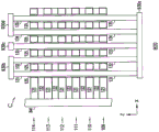
图1A展示根据本文中描述的一些实施例的包含电容器C的结构的呈IC装置100形式的设备。IC装置100可包含以下或包含于以下中:存储器装置、处理器(例如,通用处理器)、专用集成电路(ASIC)、片上系统(SoC)或其它电子(例如,半导体)装置。图1B展示图1A的电容器C的示意图。图1B的描述在描述图1A之后如下描述。FIG. 1A shows an apparatus in the form of an IC device 100 including a structure of a capacitor C, according to some embodiments described herein. IC device 100 may include or be included in a memory device, a processor (eg, a general purpose processor), an application specific integrated circuit (ASIC), a system on a chip (SoC), or other electronic (eg, semiconductor) device. FIG. 1B shows a schematic diagram of capacitor C of FIG. 1A . The description of FIG. 1B follows the description of FIG. 1A as follows.

如图1A中所展示,IC装置100可包含衬底190,在所述衬底上方(上)可形成电容器C。衬底190可包含单晶(也称为单晶体)半导体材料。举例来说,衬底190可包含单晶硅(也称为单晶体硅)。衬底190的单晶半导体材料可包含杂质,使得衬底190可具有特定导电性类型(例如,n型或p型)。衬底190可包含形成于衬底190中之电源控制电路193。电源控制电路193可包含例如晶体管、电阻器的组件和其它电路组件。衬底190还可包含为简单起见未展示的其它电路。As shown in FIG. 1A , IC device 100 may include a substrate 190 over (on) a capacitor C may be formed. Substrate 190 may comprise a single crystal (also referred to as monocrystalline) semiconductor material. For example, substrate 190 may comprise single crystal silicon (also referred to as monocrystalline silicon). The single crystal semiconductor material of substrate 190 may contain impurities such that substrate 190 may have a specific conductivity type (eg, n-type or p-type). Substrate 190 may include power control circuitry 193 formed in substrate 190 . The power control circuit 193 may include components such as transistors, resistors, and other circuit components. Substrate 190 may also include other circuitry not shown for simplicity.

如图1A中所展示,IC装置100可包含不同层级(物理内部装置层级),所述层级包含层级109到114和层级109'到113',其为在垂直于衬底190的z方向上的层级(例如,关于衬底190的竖直层级)。电容器C可包含位于层级109到114中的导电材料121和位于层级109'到113'中的电介质材料122。如图1A中所展示,导电材料121(例如,竖直隔开的导电材料层)和电介质材料122(例如,竖直隔开的电介质材料层)形成于交错布置(例如,交叉布置)中,使得导电材料121中的一种可在电介质材料122的两种之间,且电介质材料122中的一种可在导电材料121的两种之间。导电材料121可包含金属、经导电掺杂的多晶硅或其它导电材料。电介质材料122可包含氧化物材料(例如,二氧化硅SiO2)。As shown in FIG. 1A , IC device 100 may include different levels (physical internal device levels) including levels 109 to 114 and levels 109' to 113', which are in the z-direction perpendicular to substrate 190. Hierarchy (eg, vertical hierarchy with respect to substrate 190). Capacitor C may include conductive material 121 in levels 109-114 and dielectric material 122 in levels 109'-113'. As shown in FIG. 1A , conductive material 121 (e.g., vertically spaced layers of conductive material) and dielectric material 122 (e.g., vertically spaced layers of dielectric material) are formed in an interleaved arrangement (e.g., a crossed arrangement), So that one of the conductive materials 121 can be between two kinds of dielectric materials 122 , and one of the dielectric materials 122 can be between two kinds of conductive materials 121 . The conductive material 121 may include metal, conductively doped polysilicon, or other conductive materials. The dielectric material 122 may include an oxide material (eg, silicon dioxide SiO 2 ).

图1A展示六种导电材料121(例如,导电材料121的六个层)和五种电介质材料122(例如,电介质材料122的五个层)的交错布置的一实例。然而,视IC装置100的电容器C的层(例如,在z方向上的导电材料121和电介质材料122的竖直层)的数量而定,导电材料121的数量(例如,导电材料121的层的数量)和电介质材料122的数量(例如,电介质材料122的层的数量)可变化。IC装置100的电容器C的层可包含导电材料121中的一种和邻近的电介质材料122中的一种。举例来说,图1A展示其中导电材料121和电介质材料122可包含于IC装置100的电容器C中的六个层中的一实例。FIG. 1A shows an example of an interleaved arrangement of six conductive materials 121 (eg, six layers of conductive material 121 ) and five dielectric materials 122 (eg, five layers of dielectric material 122 ). However, depending on the number of layers (e.g., vertical layers of conductive material 121 and dielectric material 122 in the z-direction) of capacitor C of IC device 100, the amount of conductive material 121 (e.g., the number of layers of conductive material 121 amount) and the amount of dielectric material 122 (eg, the number of layers of dielectric material 122 ) may vary. The layers of capacitor C of IC device 100 may include one of conductive materials 121 and an adjacent one of dielectric materials 122 . For example, FIG. 1A shows an example of six layers in which conductive material 121 and dielectric material 122 may be included in capacitor C of IC device 100 .

如图1A中所展示,电容器C可包含穿过电容器C的层(例如,穿过z方向上的导电材料121和电介质材料122)的导电触点131到135(导电柱结构)。举例来说,导电触点131到135中的每一个可具有在垂直于层级109到114和109'到113'的方向(例如,z方向)上延伸的长度。电容器C可包含孔(例如,竖直沟槽)150。在图1A中,为简单起见,仅标签孔150中的两个。孔150中的每一个可延伸穿过导电材料121和电介质材料122。举例来说,孔150中的每一个可包含延伸穿过导电材料121和电介质材料122的竖直壁(例如,侧壁)。导电触点131到135中的每一个可包含相应孔150内部的部分。导电触点131到135可包含金属、经导电掺杂的多晶硅或其它导电材料。导电触点131到135中的每一个可通过相应的电介质材料125(例如,电容器电介质)与导电材料121电分离(例如,电隔离或电绝缘),所述电介质材料可包含氧化物材料(例如,二氧化硅SiO2)。As shown in FIG. 1A , capacitor C may include conductive contacts 131 - 135 (conductive post structures) through the layers of capacitor C (eg, through conductive material 121 and dielectric material 122 in the z-direction). For example, each of conductive contacts 131-135 may have a length extending in a direction (eg, the z-direction) perpendicular to levels 109-114 and 109'-113'. Capacitor C may include holes (eg, vertical trenches) 150 . In FIG. 1A, only two of the label holes 150 are shown for simplicity. Each of holes 150 may extend through conductive material 121 and dielectric material 122 . For example, each of holes 150 may include vertical walls (eg, sidewalls) extending through conductive material 121 and dielectric material 122 . Each of the conductive contacts 131 - 135 may include a portion inside the corresponding hole 150 . Conductive contacts 131-135 may comprise metal, conductively doped polysilicon, or other conductive materials. Each of the conductive contacts 131-135 may be electrically separated (eg, electrically isolated or electrically insulated) from the conductive material 121 by a corresponding dielectric material 125 (eg, a capacitor dielectric), which may include an oxide material (eg, a capacitor dielectric). , silicon dioxide SiO 2 ).

电容器C可包含穿过电容器C的层(例如,穿过z方向上的导电材料121和电介质材料122)的导电触点141(导电柱结构)。图1A中所展示的导电触点141是展示于图1C中(下文详细描述)的多个导电触点141(y方向上)中的一个。如图1A中所展示,导电触点141可具有在垂直于层级109到114和109'到113'的方向(例如,z方向)上延伸的长度。导电触点141可包含相应孔150内部的部分。导电触点141可包含与导电触点131到135相同的材料(或与其不同的材料)。举例来说,导电触点141可包含金属、经导电掺杂的多晶硅或其它导电材料。不同于导电触点131到135中的每一个和导电触点141,电介质材料(例如,电介质材料125)可不在导电触点141与导电材料121之间。因此,导电触点141不与导电材料121电分离(不与其电隔离)。导电触点141可接触(可电耦合到)一组(一些或所有)导电材料121。图1A展示其中导电触点141接触所有导电材料121的一实例。然而,导电触点141可接触少于所有导电材料121。因此,导电触点141可接触一组导电材料121,其中所述组导电材料121可包含所有导电材料121或少于所有(例如,仅部分)导电材料121。Capacitor C may include conductive contacts 141 (conductive post structures) through the layers of capacitor C (eg, through conductive material 121 and dielectric material 122 in the z-direction). The conductive contact 141 shown in FIG. 1A is one of a plurality of conductive contacts 141 (in the y-direction) shown in FIG. 1C (described in detail below). As shown in FIG. 1A , conductive contacts 141 may have lengths that extend in a direction (eg, the z-direction) perpendicular to levels 109-114 and 109'-113'. The conductive contacts 141 may include portions inside the corresponding holes 150 . Conductive contact 141 may comprise the same material (or a different material) than conductive contacts 131 - 135 . For example, the conductive contacts 141 may comprise metal, conductively doped polysilicon, or other conductive materials. Unlike each of conductive contacts 131 - 135 and conductive contact 141 , a dielectric material (eg, dielectric material 125 ) may not be between conductive contact 141 and conductive material 121 . Accordingly, conductive contacts 141 are not electrically separated from (not electrically isolated from) conductive material 121 . Conductive contacts 141 may contact (can be electrically coupled to) set (some or all) of conductive material 121 . FIG. 1A shows an example where conductive contacts 141 contact all of conductive material 121 . However, conductive contacts 141 may contact less than all of conductive material 121 . Accordingly, the conductive contacts 141 may contact a set of conductive materials 121 , wherein the set of conductive materials 121 may include all of the conductive materials 121 or less than all (eg, only some) of the conductive materials 121 .

类似地,导电触点141可接触一组(一些或所有)电介质材料122。图1A展示其中导电触点141接触所有电介质材料122的一实例。然而,导电触点141可接触少于所有电介质材料122。因此,导电触点141可接触一组电介质材料122,其中所述组电介质材料122可包含所有电介质材料122或少于所有(例如,仅部分)电介质材料122。Similarly, conductive contacts 141 may contact a set (some or all) of dielectric material 122 . FIG. 1A shows an example where conductive contacts 141 contact all of dielectric material 122 . However, conductive contacts 141 may contact less than all of dielectric material 122 . Accordingly, the conductive contacts 141 may contact a set of dielectric materials 122 , where the set of dielectric materials 122 may include all of the dielectric material 122 or less than all (eg, only some) of the dielectric material 122 .

如图1A中所展示,电容器C可包含导电区(例如,顶部导电区)130和140,和导电区(例如,底部导电区)191和192。导电区191和192彼此电分离。导电区130和140彼此电分离。导电区130和140中的每一个可以是导电线(例如,金属线)的部分。导电区191和192中的每一个可以是导电线(例如,经导电掺杂的多晶硅)的部分。As shown in FIG. 1A , capacitor C may include conductive regions (eg, top conductive regions) 130 and 140 , and conductive regions (eg, bottom conductive regions) 191 and 192 . Conductive regions 191 and 192 are electrically separated from each other. Conductive regions 130 and 140 are electrically separated from each other. Each of the conductive regions 130 and 140 may be part of a conductive line (eg, a metal line). Each of conductive regions 191 and 192 may be part of a conductive line (eg, conductively doped polysilicon).

如图1A中所展示,导电区130可接触(可电耦合到)导电触点131到135中的每一个的末端(例如,顶部端)处的导电触点131到135。因此,导电触点131到135可通过导电区130电耦合到彼此。As shown in FIG. 1A , conductive region 130 can contact (can be electrically coupled to) conductive contacts 131 - 135 at an end (eg, top end) of each of conductive contacts 131 - 135 . Accordingly, conductive contacts 131 - 135 may be electrically coupled to each other through conductive region 130 .

导电区140可接触(可电耦合到)导电触点141的末端(例如,顶部端)处的导电触点141。Conductive region 140 may contact (can be electrically coupled to) conductive contact 141 at an end (eg, top end) of conductive contact 141 .

导电区192可接触(可电耦合到)导电触点131到135中的每一个的末端(例如,底端)处的导电触点131到135。导电区191可接触(可电耦合到)导电触点141的末端(例如,底部端)处的导电触点141。Conductive region 192 may contact (can be electrically coupled to) conductive contacts 131 - 135 at an end (eg, bottom end) of each of conductive contacts 131 - 135 . Conductive region 191 may contact (can be electrically coupled to) conductive contact 141 at an end (eg, bottom end) of conductive contact 141 .

如图1A中所展示,IC装置100可包含导电路径130'和140'。导电路径130'可提供电容器C的导电触点131到135与电源控制电路193之间的电连接(例如,电流路径)。导电路径140'可提供电容器C的导电触点141与电源控制电路193之间的电气连接(例如,电流路径)。As shown in FIG. 1A , IC device 100 may include conductive paths 130' and 140'. The conductive path 130 ′ may provide an electrical connection (eg, a current path) between the conductive contacts 131 - 135 of the capacitor C and the power control circuit 193 . The conductive path 140 ′ may provide an electrical connection (eg, a current path) between the conductive contact 141 of the capacitor C and the power control circuit 193 .

为简单起见,图1A象征性地将导电路径130'和140'展示为虚线。然而,导电路径130'和140'的结构可包含物理尺寸(例如,可具有长度、宽度和厚度的结构)和导电材料(例如,金属、经导电掺杂的多晶硅或其它导电材料)。导电路径130'可电连接到导电区130。因此,导电路径130'可通过导电区130电耦合到导电触点131到135。导电路径140'可电耦合到导电区140。因此,导电路径140'可通过导电区140电耦合到导电触点141。For simplicity, FIG. 1A symbolically shows conductive paths 130' and 140' as dashed lines. However, the structure of conductive paths 130' and 140' may include physical dimensions (eg, structures that may have length, width, and thickness) and conductive materials (eg, metal, conductively doped polysilicon, or other conductive material). The conductive path 130 ′ may be electrically connected to the conductive region 130 . Accordingly, conductive path 130 ′ may be electrically coupled to conductive contacts 131 - 135 through conductive region 130 . Conductive path 140 ′ may be electrically coupled to conductive region 140 . Accordingly, conductive path 140 ′ may be electrically coupled to conductive contact 141 through conductive region 140 .

图1B展示根据本文中描述的一些实施例的包含电容器C和电容器节点(例如,电容器终端)130”和140”的图1A的IC装置100的部分的示意图。在图1A中,导电触点131到135(导电柱结构)、导电区130和导电路径130'可以是电容器节点130”(图1B)的部分(例如,或替代地可耦合到所述电容器节点130”)。图1A的导电触点141(导电柱结构)、导电区140和导电路径140'可以是电容器节点140”(图1B)的部分(例如,或替代地可耦合到所述电容器节点140”)。图1A的导电材料121可以是电容器C的板片的部分。如图1B中所展示,电容器节点130”和140”可分别通过导电路径130'和140'耦合到电源控制电路193。电容器C可用于低压操作(例如,1V到5V的电压)或高压操作(例如,大于5V的电压)。因此,电容器节点130”和140”可被配置成在低压或高压(1V到20V或更高的电压范围,视用于IC装置100中的电容器C的功能而定)操作。FIG. 1B shows a schematic diagram of a portion of IC device 100 of FIG. 1A including capacitor C and capacitor nodes (eg, capacitor terminals) 130 ″ and 140 ″, according to some embodiments described herein. In FIG. 1A, conductive contacts 131 to 135 (conductive post structures), conductive region 130, and conductive path 130' may be part of (eg, or alternatively may be coupled to) capacitor node 130" (FIG. 1B ). 130"). Conductive contact 141 (conductive post structure), conductive region 140 and conductive path 140' of FIG. 1A may be part of (eg, or alternatively may be coupled to) capacitor node 140" (FIG. 1B). Conductive material 121 of FIG. 1A may be part of a plate of capacitor C. Referring to FIG. As shown in FIG. 1B, capacitor nodes 130" and 140" may be coupled to power control circuitry 193 through conductive paths 130' and 140', respectively. Capacitor C can be used for low voltage operation (eg, voltages of 1V to 5V) or high voltage operation (eg, voltages greater than 5V). Accordingly, capacitor nodes 130 ″ and 140 ″ may be configured to operate at low voltage or high voltage (voltage range of 1V to 20V or higher, depending on the function of capacitor C used in IC device 100 ).

如图1B中所展示,电源控制电路193可包含(或可耦合到)节点180、181和182。节点180和181可分别接收电压V0和V1。电压V1可具有比电压V0更高的值(以伏特单位计)。作为一实例,电压V1可为IC装置100的供电电压(例如,Vcc),且电压V0可以接地(例如,Vss)。节点182可提供电压VOUT。电源控制电路193可操作,使得电压VOUT可具有负值(例如,可小于电压V0)或正值(例如,可为更大的电压V1)。作为一实例,电源控制电路193可包含电荷泵,使得节点182可为电荷泵的输出节点。电荷泵可为正电荷泵,使得电压VOUT的值可为正值(例如,可为更大的IC装置100的供电电压)。As shown in FIG. 1B , power control circuitry 193 may include (or may be coupled to) nodes 180 , 181 , and 182 . Nodes 180 and 181 may receive voltages V0 and V1, respectively. Voltage V1 may have a higher value (in units of volts) than voltage V0. As an example, the voltage V1 may be a supply voltage of the IC device 100 (eg, Vcc), and the voltage V0 may be grounded (eg, Vss). Node 182 may provide a voltage V OUT . The power control circuit 193 is operable such that the voltage V OUT can have a negative value (eg, can be less than the voltage V0 ) or a positive value (eg, can be a larger voltage V1 ). As an example, power control circuit 193 may include a charge pump such that node 182 may be an output node of the charge pump. The charge pump may be a positive charge pump such that the value of voltage V OUT may be positive (eg, may be a larger supply voltage for IC device 100 ).

图1A和图1B展示作为一实例的仅包含一个电容器C的IC装置100。然而,IC装置100可包含多个电容器C,其中所述多个电容器C可形成IC装置100的电荷泵(例如,多级电荷泵)的多个级。1A and 1B show an IC device 100 including only one capacitor C as an example. However, IC device 100 may include multiple capacitors C, where the multiple capacitors C may form multiple stages of a charge pump (eg, a multi-stage charge pump) of IC device 100 .

图1C展示根据本文中描述的一些实施例的包含位于IC装置100的其它其它元件上方的导电区130和140的图1A的IC装置100的部分顶视图。如图1C中所展示,导电区130可位于导电材料121和孔150上方,且可接触(可电耦合到)导电触点131到135(是位于导电区130下的孔150中)。图1C展示作为一实例的是一片(例如,单片)导电材料的导电区130。在IC装置100的替代结构中,导电区130可包含多片(例如,多个分离导电区)导电材料(例如,可由所述多片导电材料形成),所述多片导电材料可接触(可电耦合到)相应导电触点131到135。在替代结构中,多片导电材料可电耦合到彼此,使得导电触点131到135可通过多片导电材料电耦合到彼此。FIG. 1C shows a partial top view of the IC device 100 of FIG. 1A including conductive regions 130 and 140 located above other elements of the IC device 100 according to some embodiments described herein. As shown in FIG. 1C , conductive region 130 may be located over conductive material 121 and hole 150 , and may contact (could be electrically coupled to) conductive contacts 131 - 135 in hole 150 under conductive region 130 . FIG. 1C shows conductive region 130 that is a sheet (eg, monolithic) of conductive material as an example. In alternative configurations for IC device 100, conductive region 130 may comprise (e.g., may be formed from) multiple sheets (e.g., multiple separate conductive regions) of conductive material that may contact (e.g., electrically coupled to) corresponding conductive contacts 131-135. In an alternative configuration, multiple pieces of conductive material may be electrically coupled to each other such that conductive contacts 131 - 135 may be electrically coupled to each other through multiple pieces of conductive material.

如图1C中所展示,导电区140可位于导电材料121上方和一组孔150(例如,最左孔150)上方且可接触(可电耦合到)导电触点141(其位于导电区140下的孔150中)。导电区140可为一片(例如,单片)导电材料。导电区140可接触(可电耦合到)导电触点141中的每一个的末端(例如,顶部端)处的导电触点141。因此,导电触点141(如图1C中所展示)可通过导电区140电耦合到彼此。As shown in FIG. 1C , conductive region 140 may be located above conductive material 121 and over a set of holes 150 (e.g., leftmost hole 150) and may contact (could be electrically coupled to) conductive contact 141 (which is located below conductive region 140). in the hole 150). Conductive region 140 may be a piece (eg, monolithic) of conductive material. Conductive region 140 may contact (can be electrically coupled to) conductive contact 141 at an end (eg, top end) of each of conductive contacts 141 . Accordingly, conductive contacts 141 (as shown in FIG. 1C ) can be electrically coupled to each other through conductive region 140 .

如图1C中所展示,孔150可布置于x方向和y方向(例如,垂直于z方向的平面)上的行和列中。图1C象征性地将导电路径130'和140'展示为虚线。然而,如上文所提及,导电路径130'和140'中的每一个可包含导电材料以提供电源控制电路193(图1A)与相应导电触点141和131到135(图1C)之间的电导。As shown in FIG. 1C , holes 150 may be arranged in rows and columns in the x-direction and y-direction (eg, a plane perpendicular to the z-direction). Figure 1C symbolically shows conductive paths 130' and 140' as dashed lines. However, as mentioned above, each of the conductive paths 130' and 140' may comprise a conductive material to provide communication between the power control circuit 193 (FIG. 1A) and the corresponding conductive contacts 141 and 131-135 (FIG. 1C). conductance.

图1D展示根据本文中描述的一些实施例的包含孔150和导电触点131到135和141的相应部分的层级114处的图1A的IC装置100的部分顶视图。如图1D中所展示,导电触点131到135中的每一个可包含形成于导电材料121中的相应孔150中的部分且可通过相应电介质材料125与导电材料121电分离。在接触导电区130的特定孔中(孔150中),电介质材料125可形成于特定孔的壁(例如,侧壁)上且可包围导电触点131到135中的相应导电触点。在接触导电区140的特定孔中(孔150中),电介质材料125可形成于特定孔的壁(例如,侧壁)上且可包围导电触点141中的相应导电触点。1D shows a partial top view of IC device 100 of FIG. 1A at level 114 including holes 150 and respective portions of conductive contacts 131 - 135 and 141 , according to some embodiments described herein. As shown in FIG. 1D , each of conductive contacts 131 - 135 may include a portion formed in a respective hole 150 in conductive material 121 and may be electrically separated from conductive material 121 by a respective dielectric material 125 . In a particular hole that contacts conductive region 130 (in hole 150 ), dielectric material 125 may be formed on a wall (eg, sidewall) of the particular hole and may surround a corresponding one of conductive contacts 131 - 135 . In particular holes that contact conductive regions 140 (in holes 150 ), dielectric material 125 may be formed on walls (eg, sidewalls) of the particular holes and may surround corresponding ones of conductive contacts 141 .

图1E展示根据本文中描述的一些实施例的包含孔150和导电触点131到135和141的相应部分的层级113处的图1A的IC装置100的部分顶视图。如图1E中所展示,层级113处的图1E的IC装置100的结构与层级114(展示于图1D中)处的IC装置100的结构相同。因此,不重复图1D和图1E的IC装置100的相同元件的详细描述。层级109、110、111和112处的图1A的IC装置100的结构与层级114(图1D)和层级113(图1E)处的图1A的IC装置100的结构相同。FIG. 1E shows a partial top view of IC device 100 of FIG. 1A at level 113 including holes 150 and respective portions of conductive contacts 131 - 135 and 141 , according to some embodiments described herein. As shown in Figure IE, the structure of the IC device 100 of Figure IE at level 113 is the same as the structure of the IC device 100 at level 114 (shown in Figure ID). Therefore, detailed descriptions of the same elements of the IC device 100 of FIGS. 1D and 1E are not repeated. The IC device 100 of FIG. 1A at levels 109 , 110 , 111 , and 112 has the same structure as the IC device 100 of FIG. 1A at levels 114 ( FIG. 1D ) and 113 ( FIG. 1E ).

图1A展示作为一实例的位于IC装置100的某些位置(例如,某些层级)中的导电区130、140、191和192。然而,导电区130和140可位于不同于图1A中所展示的位置的位置中。FIG. 1A shows conductive regions 130 , 140 , 191 , and 192 located in certain locations (eg, certain levels) of IC device 100 as an example. However, conductive regions 130 and 140 may be located in locations other than that shown in FIG. 1A .

以下描述论述与图1A到图1E的IC装置100的电容器C类似(例如,可为其变型)的额外电容器。因此,为简单起见,本文描述中的类似或相同元件被赋予相同标签,且不重复类似或相同元件的详细描述。同样为简单起见,从附图中省略本文中所描述的IC装置的一些元件(例如,导电触点131到135和电介质材料125)的横截面线。The following description discusses additional capacitors similar to (eg, variations on) capacitor C of IC device 100 of FIGS. 1A-1E . Therefore, for simplicity, similar or identical elements in the description herein are given the same labels, and detailed descriptions of similar or identical elements are not repeated. Also for simplicity, cross-sectional lines of some elements of the IC devices described herein (eg, conductive contacts 131-135 and dielectric material 125) are omitted from the figures.

图2A展示根据本文中描述的一些实施例的包含具有位于IC装置200的不同层级中的导电区140和230的电容器C的结构的呈IC装置200形式的设备。导电区140和230彼此电分离。下文描述IC装置100(图1A)与IC装置200(图2A)之间的结构差异。2A shows an apparatus in the form of an IC device 200 including a structure including a capacitor C with conductive regions 140 and 230 located in different levels of the IC device 200, according to some embodiments described herein. Conductive regions 140 and 230 are electrically separated from each other. Structural differences between IC device 100 (FIG. 1A) and IC device 200 (FIG. 2A) are described below.

在图1A中,导电区130和140可位于IC装置100的相同层级(例如,层级114上的层级)中。举例来说,在图1A中,导电区130和140中的每一个可接触位于层级114上的层级中的末端(例如,相应导电触点的部分)处的相应导电触点。在图2A中,导电区140和230可位于IC装置200的不同层级中。举例来说,导电区230可接触位于层级109下的层级(其在层级114下)中的相应导电触点的末端处的每个相应导电触点(131到135)。IC装置200可包含导电路径230'以提供导电区230与电源控制电路193之间的电连接。为简单起见,图2A象征性地将导电路径230'展示为虚线。然而,导电路径230'的结构可包含物理尺寸(例如,可具有长度、宽度和厚度的结构)和导电材料(例如,金属、经导电掺杂的多晶硅或其它导电材料)。In FIG. 1A , conductive regions 130 and 140 may be located in the same level of IC device 100 (eg, a level above level 114 ). For example, in FIG. 1A , each of conductive regions 130 and 140 may contact a respective conductive contact located at an end (eg, portion of a respective conductive contact) in a level above level 114 . In FIG. 2A , conductive regions 140 and 230 may be located in different levels of IC device 200 . For example, conductive region 230 may contact each respective conductive contact ( 131 - 135 ) at the end of a respective conductive contact located in a level below level 109 (which is below level 114 ). IC device 200 may include a conductive path 230 ′ to provide electrical connection between conductive region 230 and power control circuit 193 . For simplicity, FIG. 2A symbolically shows conductive path 230' as a dashed line. However, the structure of the conductive path 230' may include physical dimensions (eg, a structure that may have a length, width, and thickness) and conductive material (eg, metal, conductively doped polysilicon, or other conductive material).

图2B展示根据本文中描述的一些实施例的包含电容器C和电容器节点230”的图2A的IC装置200的部分的示意图。在图2A中,图2A的导电触点131到135、导电区230和导电路径230'可以是电容器节点(例如,电容器终端)230”(图2B)的部分(例如,或替代地可耦合到所述电容器节点230”)。2B shows a schematic diagram of the portion of IC device 200 of FIG. 2A including capacitor C and capacitor node 230″, according to some embodiments described herein. In FIG. 2A, conductive contacts 131-135, conductive region 230 of FIG. 2A And conductive path 230' may be part of (eg, or alternatively may be coupled to) capacitor node (eg, capacitor terminal) 230" (FIG. 2B).

图2C展示根据本文中描述的一些实施例的包含位于IC装置200的导电触点131到135下的导电区230的图2A的IC装置200的部分顶视图。如图2C中所展示,导电区230可位于导电材料121和孔150下。图2C展示作为一实例的是一片(例如,单片)导电材料的导电区230。在IC装置200的替代结构中,导电区230可包含多片(例如,多个分离导电区)导电材料(例如,可由所述多片导电材料形成),所述多片导电材料可接触(例如,可电耦合到)相应导电触点131到135。在替代结构中,多片导电材料可电耦合到彼此,使得导电触点131到135可通过多片导电材料电耦合到彼此。2C shows a partial top view of the IC device 200 of FIG. 2A including a conductive region 230 located under the conductive contacts 131-135 of the IC device 200, according to some embodiments described herein. As shown in FIG. 2C , conductive region 230 may be located under conductive material 121 and hole 150 . FIG. 2C shows conductive region 230 that is a sheet (eg, monolithic) of conductive material as an example. In alternative configurations for IC device 200, conductive region 230 may comprise (e.g., may be formed from) multiple sheets (e.g., a plurality of separate conductive regions) of conductive material that may contact (e.g., , can be electrically coupled to) corresponding conductive contacts 131 to 135. In an alternative configuration, multiple pieces of conductive material may be electrically coupled to each other such that conductive contacts 131 - 135 may be electrically coupled to each other through multiple pieces of conductive material.

图3A展示根据本文中描述的一些实施例的包含具有位于IC装置300的不同层级中的导电区130和340的电容器C的结构的呈IC装置300形式的设备。导电区140和340彼此电分离。下文描述IC装置100(图1A)与IC装置300(图3A)之间的结构差异。3A shows an apparatus in the form of an IC device 300 including a structure including a capacitor C with conductive regions 130 and 340 located in different levels of the IC device 300, according to some embodiments described herein. Conductive regions 140 and 340 are electrically separated from each other. Structural differences between IC device 100 (FIG. 1A) and IC device 300 (FIG. 3A) are described below.

如上文参看图1A所描述,导电区130和140可位于IC装置100的相同层级(例如,层级114上的层级)中。在图3A中,导电区130和340可位于IC装置200的不同层级中。举例来说,导电区340可接触位于层级109下的层级(其在层级114下)的导电触点141的末端处的导电触点141。IC装置300可包含导电路径340'以提供导电区340与电源控制电路193之间的电连接。为简单起见,图3A象征性地将导电路径340'展示为虚线。然而,导电路径340'的结构可包含物理尺寸(例如,可具有长度、宽度和厚度的结构)和导电材料(例如,金属、经导电掺杂的多晶硅或其它导电材料)。As described above with reference to FIG. 1A , conductive regions 130 and 140 may be located in the same level of IC device 100 (eg, a level above level 114 ). In FIG. 3A , conductive regions 130 and 340 may be located in different levels of IC device 200 . For example, conductive region 340 may contact conductive contact 141 at the end of conductive contact 141 at a level below level 109 that is below level 114 . IC device 300 may include a conductive path 340 ′ to provide electrical connection between conductive region 340 and power control circuit 193 . For simplicity, FIG. 3A symbolically shows conductive path 340' as a dashed line. However, the structure of conductive pathway 340' may include physical dimensions (eg, a structure that may have a length, width, and thickness) and conductive material (eg, metal, conductively doped polysilicon, or other conductive material).

图3B展示根据本文中描述的一些实施例的包含电容器C和电容器节点340”的图3A的IC装置300的部分的示意图。在图3A中,图3A的导电触点141、导电区340和导电路径340'可以是电容器节点340”(图3B)的部分(例如,或替代地可耦合到所述电容器节点340”)。3B shows a schematic diagram of the portion of IC device 300 of FIG. 3A including capacitor C and capacitor node 340″, according to some embodiments described herein. In FIG. 3A, conductive contact 141, conductive region 340, and conductive Path 340' may be part of (eg, or alternatively may be coupled to) capacitor node 340" (FIG. 3B).

图3C展示根据本文中描述的一些实施例的包含位于IC装置300的导电触点141下的导电区340的图3A的IC装置300的部分顶视图。导电区130可以是图1C中的相同导电区130。3C shows a partial top view of the IC device 300 of FIG. 3A including a conductive region 340 located under a conductive contact 141 of the IC device 300 according to some embodiments described herein. Conductive region 130 may be the same conductive region 130 in FIG. 1C.

图4A展示根据本文中描述的一些实施例的包含具有位于IC装置400的导电材料121的相同层级中和所述IC装置400的所述导电材料121下的导电区430和440的电容器C的结构的呈IC装置400形式的设备。导电区430和440彼此电分离。下文描述IC装置100(图1A)与IC装置400(图4A)之间的结构差异。4A shows a structure including a capacitor C having conductive regions 430 and 440 located in the same level of conductive material 121 of IC device 400 and under the conductive material 121 of IC device 400, according to some embodiments described herein. An apparatus in the form of an IC device 400 . Conductive regions 430 and 440 are electrically separated from each other. Structural differences between IC device 100 (FIG. 1A) and IC device 400 (FIG. 4A) are described below.

在图1A中,导电区130和140可位于IC装置100的层级114上的相同层级中。在图4A中,导电区430和440也位于相同层级中。然而,导电区430和440在IC装置400的层级114下。IC装置400可包含导电路径430'以提供导电区430与电源控制电路193之间的电连接。IC装置400可包含导电路径440'以提供导电区440与电源控制电路193之间的电连接。为简单起见,图4A象征性地将导电路径430'和440'中的每一个展示为虚线。然而,导电路径430'和440'中的每一个的结构可包含物理尺寸(例如,可具有长度、宽度和厚度的结构)和导电材料(例如,金属、经导电掺杂的多晶硅或其它导电材料)。In FIG. 1A , conductive regions 130 and 140 may be located in the same level above level 114 of IC device 100 . In FIG. 4A, conductive regions 430 and 440 are also located in the same level. However, conductive regions 430 and 440 are below level 114 of IC device 400 . IC device 400 may include a conductive path 430 ′ to provide electrical connection between conductive region 430 and power control circuit 193 . IC device 400 may include a conductive path 440 ′ to provide electrical connection between conductive region 440 and power control circuit 193 . For simplicity, FIG. 4A symbolically shows each of conductive paths 430' and 440' as dashed lines. However, the structure of each of conductive paths 430' and 440' may include physical dimensions (eg, structures that may have length, width, and thickness) and conductive materials (eg, metal, conductively doped polysilicon, or other conductive material ).

图4B展示根据本文中描述的一些实施例的包含电容器C和电容器节点430”和440”的图4A的IC装置400的部分的示意图。在图4A中,图4A的导电触点131到135、导电区430和导电路径430'可以是电容器节点430”(图4B)的部分(例如,或替代地可耦合到所述电容器节点430”)。图4A的导电触点141、导电区440和导电路径440'可以是电容器节点440”(图4B)的部分(例如,或替代地可耦合到所述电容器节点440”)。FIG. 4B shows a schematic diagram of the portion of IC device 400 of FIG. 4A including capacitor C and capacitor nodes 430 ″ and 440 ″, according to some embodiments described herein. In FIG. 4A, conductive contacts 131 through 135, conductive region 430, and conductive path 430' of FIG. 4A may be part of (eg, or alternatively may be coupled to, capacitor node 430" (FIG. 4B) ). Conductive contact 141, conductive region 440, and conductive path 440' of FIG. 4A may be part of (eg, or alternatively may be coupled to) capacitor node 440" (FIG. 4B).

图4C展示根据本文中描述的一些实施例的包含位于导电触点131到135下的导电区430和位于IC装置400的导电触点141下的导电区440的图4A的IC装置400的部分顶视图。如图4C中所展示,导电区430可位于导电材料121和孔150下。图4C展示作为一实例的是一片(例如,单件)导电材料的导电区430。在IC装置400的替代结构中,导电区430可包含多片(例如,多个分离导电区)导电材料(例如,可由所述多片导电材料形成),所述多片导电材料可接触(例如,可电耦合到)相应导电触点131到135。在替代结构中,多片导电材料可电耦合到彼此,使得导电触点131到135可通过多片导电材料电耦合到彼此。4C shows a partial top view of IC device 400 of FIG. 4A including conductive region 430 under conductive contacts 131-135 and conductive region 440 under conductive contact 141 of IC device 400, according to some embodiments described herein. view. As shown in FIG. 4C , conductive region 430 may be located under conductive material 121 and hole 150 . FIG. 4C shows a conductive region 430 that is a sheet (eg, a single piece) of conductive material as an example. In alternative configurations for IC device 400, conductive region 430 may comprise (e.g., may be formed from) multiple sheets (e.g., a plurality of separate conductive regions) of conductive material that may contact (e.g., , can be electrically coupled to) corresponding conductive contacts 131 to 135. In an alternative configuration, multiple pieces of conductive material may be electrically coupled to each other such that conductive contacts 131 - 135 may be electrically coupled to each other through multiple pieces of conductive material.

图5A展示根据本文中描述的一些实施例的包含具有导电区191、192、430和440的电容器C的结构的呈IC装置500形式的设备。IC装置400与500之间的结构差异包含图5A中的导电区191和192的添加。在IC装置500的结构中,导电区191和192(其也存在于图1A的IC装置100中)可以是导线(例如,源极,未展示)的部分以将信号携载到IC装置500的其它组件(未展示)。导电区191和192可以是这些导线的未使用部分且可保留在电容器C的导电材料121下。因此,如图5A中所展示,导电触点131到135可穿过导电区192且接触导电区430。导电触点131到135可或可不电耦合到(例如,可或可不接触)导电区192。类似地,导电触点141可穿过导电区191且接触导电区440。导电触点141可或可不电耦合到(例如,可或可不接触)导电区191。Figure 5A shows an apparatus in the form of an IC device 500 including a structure of a capacitor C having conductive regions 191, 192, 430, and 440, according to some embodiments described herein. The structural differences between IC devices 400 and 500 include the addition of conductive regions 191 and 192 in Figure 5A. In the structure of IC device 500, conductive regions 191 and 192 (which are also present in IC device 100 of FIG. other components (not shown). Conductive regions 191 and 192 may be unused portions of these wires and may remain under the conductive material 121 of capacitor C. Accordingly, conductive contacts 131 - 135 may pass through conductive region 192 and contact conductive region 430 as shown in FIG. 5A . Conductive contacts 131 - 135 may or may not be electrically coupled to (eg, may or may not contact) conductive region 192 . Similarly, conductive contact 141 may pass through conductive region 191 and contact conductive region 440 . Conductive contact 141 may or may not be electrically coupled to (eg, may or may not contact) conductive region 191 .

图5B展示根据本文中描述的一些实施例的包含电容器C的图5A的IC装置500的部分的示意图。图5A的IC装置500的示意图可与图4A的IC装置400的示意图相同。FIG. 5B shows a schematic diagram of a portion of the IC device 500 of FIG. 5A including capacitor C, according to some embodiments described herein. The schematic diagram of IC device 500 of FIG. 5A may be the same as the schematic diagram of IC device 400 of FIG. 4A .

图6A展示根据本文中描述的一些实施例的包含具有形成于导电材料121的边缘处的导电触点641的电容器C的结构的呈IC装置600形式的设备。下文描述IC装置100(图1A)与IC装置600(图6A)之间的结构差异。FIG. 6A shows an apparatus in the form of an IC device 600 including a structure of a capacitor C with conductive contacts 641 formed at edges of conductive material 121, according to some embodiments described herein. Structural differences between IC device 100 (FIG. 1A) and IC device 600 (FIG. 6A) are described below.

如上文参看图1A所描述,导电触点141可形成于孔(例如,孔150)中。在图6A中,导电触点641可不形成于孔中。导电触点641可形成于导电材料121的边缘(例如,最左边缘)处且可接触(可电耦合到)一组(一些或所有)导电材料121。图6A展示其中导电触点641接触所有导电材料121的一实例。然而,导电触点641可接触少于所有导电材料121。因此,导电触点641可接触一组导电材料121,其中所述组导电材料121可包含所有导电材料121或少于所有(例如,仅部分)导电材料121。As described above with reference to FIG. 1A , conductive contacts 141 may be formed in holes (eg, holes 150 ). In FIG. 6A, conductive contacts 641 may not be formed in the holes. Conductive contact 641 may be formed at an edge (eg, the leftmost edge) of conductive material 121 and may contact (can be electrically coupled to) a group (some or all) of conductive material 121 . FIG. 6A shows an example where conductive contacts 641 contact all of conductive material 121 . However, conductive contacts 641 may contact less than all of conductive material 121 . Accordingly, the conductive contacts 641 may contact a set of conductive materials 121 , where the set of conductive materials 121 may include all of the conductive materials 121 or less than all (eg, only some) of the conductive materials 121 .

IC装置600可包含导电区640,其可接触(可电耦合到)导电触点641的顶部(例如,顶部端)。IC装置600可包含导电路径640'以提供导电区640与电源控制电路193之间的电连接。为简单起见,图6A象征性地将导电路径640'展示为虚线。然而,导电路径640'的结构可包含物理尺寸(例如,可具有长度、宽度和厚度的结构)和导电材料(例如,金属、经导电掺杂的多晶硅或其它导电材料)。IC device 600 may include a conductive region 640 that may contact (can be electrically coupled to) a top (eg, top end) of conductive contact 641 . IC device 600 may include a conductive path 640 ′ to provide electrical connection between conductive region 640 and power control circuit 193 . For simplicity, FIG. 6A symbolically shows conductive path 640' as a dashed line. However, the structure of the conductive path 640' may include physical dimensions (eg, a structure that may have a length, width, and thickness) and conductive material (eg, metal, conductively doped polysilicon, or other conductive material).

图6B展示根据本文中描述的一些实施例的包含电容器C和电容器节点640”的图6A的IC装置600的部分的示意图。在图6A中,导电触点641、导电区640和导电路径640'可以是电容器节点(例如,电容器终端)640”(图6B)的部分(例如,或替代地可耦合到所述电容器节点640”)。6B shows a schematic diagram of the portion of IC device 600 of FIG. 6A including capacitor C and capacitor node 640″, according to some embodiments described herein. In FIG. 6A, conductive contact 641, conductive region 640, and conductive path 640′ may be part of (eg, or alternatively coupleable to) a capacitor node (eg, capacitor terminal) 640" (FIG. 6B).

图6C展示根据本文中描述的一些实施例的包含位于IC装置600的导电触点641下的导电区640的图6A的IC装置600的部分顶视图。如图6C中所展示,导电区640可位于导电材料121和导电触点641上方。导电触点641可不位于孔中。导电触点641可为一片(例如,单片)导电材料(例如,金属、经导电掺杂的多晶硅或其它导电材料)。导电触点641包含接触(电耦合到)导电区640的部分(例如,顶部端部分)。6C shows a partial top view of the IC device 600 of FIG. 6A including a conductive region 640 located under a conductive contact 641 of the IC device 600, according to some embodiments described herein. As shown in FIG. 6C , conductive region 640 may be located over conductive material 121 and conductive contact 641 . The conductive contacts 641 may not be located in the holes. The conductive contact 641 may be a piece (eg, monolithic) of conductive material (eg, metal, conductively doped polysilicon, or other conductive material). Conductive contact 641 includes a portion (eg, a top end portion) that contacts (electrically couples to) conductive region 640 .

图7展示根据本文中描述的一些实施例的包含具有形成于导电材料121的边缘处的导电触点741的电容器C的结构的呈IC装置700形式的设备。IC装置700可为图6A的IC装置600的变型。举例来说,IC装置700可包含可分别与图6A的IC装置600的导电触点641和导电区640类似的导电触点741和导电区740。IC装置700可包含与图1A、图2A、图3A、图4A、图5A和图6A中所展示的IC装置的那些类似的其它元件(例如,衬底导电区和导电路径)。然而,为简单起见,这些元件从图7中省略。FIG. 7 shows an apparatus in the form of an IC device 700 including a structure of a capacitor C having conductive contacts 741 formed at edges of conductive material 121 according to some embodiments described herein. IC device 700 may be a variation of IC device 600 of FIG. 6A . For example, IC device 700 may include conductive contacts 741 and conductive regions 740 that may be similar to conductive contacts 641 and conductive regions 640, respectively, of IC device 600 of FIG. 6A. IC device 700 may include other elements (eg, substrate conductive regions and conductive paths) similar to those of the IC devices shown in FIGS. 1A , 2A, 3A, 4A, 5A, and 6A. However, these elements are omitted from FIG. 7 for simplicity.

如图7中所展示,IC装置700的电容器C可包含部分705。部分705可包含为简单起见从图7中省略的其它元件。举例来说,IC装置700的电容器C的部分705可包含上文参看图1A、图2A、图3A、图4A、图5A和图6A所描述的电容器C的部分(例如,导电触点131到135相关的导电区和导电路径)。As shown in FIG. 7 , capacitor C of IC device 700 may include portion 705 . Portion 705 may include other elements omitted from FIG. 7 for simplicity. For example, portion 705 of capacitor C of IC device 700 may include portions of capacitor C (eg, conductive contacts 131 to 135 related conductive areas and conductive paths).

图8展示根据本文中描述的一些实施例的包含具有耦合到不同导电区(例如,底部导电区)830a、830b和830c的导电触点131到135的电容器C的结构的呈IC装置800形式的设备。IC装置800可包含与图1A、图2A、图3A、图4A、图5A、图6A和图7中所展示的IC装置的那些类似的其它元件(例如,衬底、导电区和导电路径)。然而,为简单起见,这些元件从图8中省略。8 shows a structure in the form of an IC device 800 including a capacitor C having conductive contacts 131 through 135 coupled to different conductive regions (e.g., bottom conductive regions) 830a, 830b, and 830c, according to some embodiments described herein. equipment. IC device 800 may include other elements (e.g., substrates, conductive regions, and conductive paths) similar to those of the IC devices shown in FIGS. . However, these elements are omitted from FIG. 8 for simplicity.

如图8中所展示,导电触点131到135中的每一个可包含接触(电耦合到)导电区830a的末端(例如,顶部端)。导电触点131到135可具有接触(电耦合到)导电区192、830b和830c中的不同导电区的末端(例如,底部端)。举例来说,导电触点132、133和134中的每一个的底部端可接触(可电耦合到)导电区192;相应导电触点131和135的底部端可分别接触导电区830b和830c。导电区830b和830c可电耦合到彼此(例如,通过额外导电区(例如,导电线)耦合到彼此,图8中未展示)。As shown in FIG. 8, each of conductive contacts 131-135 may include an end (eg, a top end) that contacts (electrically couples to) conductive region 830a. Conductive contacts 131-135 may have ends (eg, bottom ends) that contact (electrically couple to) different ones of conductive regions 192, 830b, and 830c. For example, a bottom end of each of conductive contacts 132, 133, and 134 may contact (could be electrically coupled to) conductive region 192; bottom ends of corresponding conductive contacts 131 and 135 may contact conductive regions 830b and 830c, respectively. Conductive regions 830b and 830c may be electrically coupled to each other (eg, via additional conductive regions (eg, conductive lines) not shown in FIG. 8 ).

如图8中所展示,在导电区830b与830c之间存在开放空间(例如,x方向上的空间)。因此,将导电触点131到135耦合到相应导电区192、830b和830c可以允许用于IC装置800的其它组件(未展示)的其它连接(例如,导电区830b和830c的层级处的底部导电路径)的更多空间(例如,开放空间处的空间)。As shown in FIG. 8, there is an open space (eg, a space in the x-direction) between conductive regions 830b and 830c. Accordingly, coupling conductive contacts 131-135 to respective conductive regions 192, 830b, and 830c may allow for other connections for other components (not shown) of IC device 800 (e.g., bottom conduction at the level of conductive regions 830b and 830c). paths) (for example, space at open spaces).

图9展示根据本文中描述的一些实施例的包含具有耦合到不同导电区(例如,顶部导电区)930a、930b和930c的导电触点131到135的电容器C的结构的呈IC装置900形式的设备。IC装置900可包含与图1A、图2A、图3A、图4A、图5A、图6A和图7中所展示的IC装置的那些类似的其它元件(例如,衬底、导电区和导电路径)。然而,为简单起见,这些元件从图9中省略。9 shows a structure in the form of an IC device 900 including a capacitor C having conductive contacts 131 through 135 coupled to different conductive regions (e.g., top conductive regions) 930a, 930b, and 930c, according to some embodiments described herein. equipment. IC device 900 may include other elements (e.g., substrates, conductive regions, and conductive paths) similar to those of the IC devices shown in FIGS. . However, these elements are omitted from FIG. 9 for simplicity.

如图9中所展示,导电触点131到135中的每一个可包含接触(电耦合到)导电区930a的末端(例如,底部端)。导电触点131到135可具有接触(电耦合到)导电区930a、930b和930c中的不同导电区的末端(例如,顶部端)。举例来说,导电触点131和132中的每一个的顶部端可接触(可电耦合到)导电区930b,导电触点133的顶部端可接触导电区930c,且导电触点134和135中的每一个的顶部端可接触(可电耦合到)导电区930d。导电区930a、930b和930c可电耦合到彼此(例如,通过一额外导电区(例如,导电线)或通过多个额外导电区(例如,多条导电线)耦合到彼此,图8中未展示)。As shown in FIG. 9, each of conductive contacts 131-135 may include an end (eg, a bottom end) that contacts (electrically couples to) conductive region 930a. Conductive contacts 131-135 may have ends (eg, top ends) that contact (electrically couple to) different ones of conductive regions 930a, 930b, and 930c. For example, a top end of each of conductive contacts 131 and 132 may contact (could be electrically coupled to) conductive region 930b, a top end of conductive contact 133 may contact conductive region 930c, and conductive contacts 134 and 135 may contact The top end of each of the can contact (can be electrically coupled to) the conductive region 930d. Conductive regions 930a, 930b, and 930c may be electrically coupled to each other (e.g., by an additional conductive region (e.g., conductive line) or by multiple additional conductive regions (e.g., multiple conductive lines), not shown in FIG. ).

如图9中所展示,在导电区930b、930c与930d之间存在开放空间(例如,x方向上的空间)。因此,将导电触点131到135耦合到相应导电区930b、930c和930d可以允许用于IC装置900的其它组件(未展示)的其它连接(例如,导电区930b、930c和930d的层级处的顶部导电路径)的更多空间(例如,开放空间处的空间)。As shown in FIG. 9, there is open space (eg, space in the x-direction) between conductive regions 930b, 930c, and 93Od. Accordingly, coupling conductive contacts 131-135 to respective conductive regions 930b, 930c, and 930d may allow for other connections for other components (not shown) of IC device 900 (e.g., at the level of conductive regions 930b, 930c, and 930d). more space (for example, space at the open space) for the top conductive path).

图10到图21展示根据本发明的一些实施例的在包含形成电容器的方法的形成IC装置1000的方法期间的元件的横截面图。形成IC装置1000的方法中的一些可用于形成上文参看图1A到图9所描述的IC装置中的一些(例如,IC装置100)。10-21 show cross-sectional views of elements during a method of forming an IC device 1000 including a method of forming a capacitor, according to some embodiments of the invention. Some of the methods of forming IC device 1000 may be used to form some of the IC devices described above with reference to FIGS. 1A-9 (eg, IC device 100 ).

图10展示在电介质材料1020'形成于z方向上的相应层级1009到1014中之后和在电介质材料1022'形成于z方向上的相应层级1009'到1015'中之后的IC装置1000。z方向(例如,竖直方向上)是垂直于衬底1090(例如,从所述衬底1090向外)的方向。z方向也垂直于x方向。衬底1090可与上文参看图1A所描述的衬底190类似(或与其相同)。如图10中所展示,电介质材料1020'和1022'可形成于IC装置1000的部分1095上方。为不混淆本文中所描述的实施例(例如,IC装置的结构),省略形成IC装置1000的部分1095的结构的方法。然而,熟习此项技术者可认识到部分1095可形成(例如,在电介质材料1020'和1022'形成之前形成)以包含IC装置1000的其它元件。这些其它元件可包含导电区,例如上文参看图1A到图9所描述的导电区(例如,191、192、230、340、430、440、830a、830b和930a)。10 shows IC device 1000 after dielectric material 1020' is formed in respective levels 1009-1014 in the z-direction and after dielectric material 1022' is formed in respective levels 1009'-1015' in the z-direction. The z-direction (eg, in the vertical direction) is a direction perpendicular to (eg, outward from) the substrate 1090 . The z direction is also perpendicular to the x direction. Substrate 1090 may be similar to (or identical to) substrate 190 described above with reference to FIG. 1A . As shown in FIG. 10 , dielectric material 1020 ′ and 1022 ′ may be formed over portion 1095 of IC device 1000 . The method of forming the structure of portion 1095 of IC device 1000 is omitted so as not to obscure the embodiments described herein (eg, the structure of the IC device). However, those skilled in the art will recognize that portion 1095 may be formed (eg, before dielectric material 1020 ′ and 1022 ′ are formed) to contain other elements of IC device 1000 . These other elements may include conductive regions such as those described above with reference to FIGS. 1A-9 (eg, 191 , 192 , 230 , 340 , 430 , 440 , 830a , 830b , and 930a ).

在图10中,形成电介质材料1020'和1022'可包含在衬底1090上方(例如,在衬底1090的部分1095上方)沉积交错的相应层级1009到1014和1009'到1015'中的电介质材料(例如,交错的电介质材料1020'的层和电介质材料1022'的层)。电介质材料1020'可包含氮化物材料(例如,亚硝酸硅SiNO4)。电介质材料1022'可包含氧化物材料(例如,二氧化硅SiO2)。In FIG. 10, forming dielectric material 1020' and 1022' may include depositing dielectric material in alternating respective levels 1009 to 1014 and 1009' to 1015' over substrate 1090 (eg, over portion 1095 of substrate 1090). (eg, alternating layers of dielectric material 1020' and layers of dielectric material 1022'). The dielectric material 1020' may include a nitride material (eg, silicon nitrite SiNO 4 ). The dielectric material 1022' may include an oxide material (eg, silicon dioxide SiO 2 ).

图10展示13种交错的电介质材料1020'和1022'的一实例(例如,13个交错的电介质材料1020'和1022'的层)。电介质材料1020'和1022'的数量(例如,交错的电介质材料1020'和1022'的层的数量)可不同于13,视将形成于IC装置1000中的电容器(例如,图20中的电容器C)的层的数量而定。FIG. 10 shows an example of 13 interleaved dielectric materials 1020' and 1022' (eg, 13 layers of interleaved dielectric materials 1020' and 1022'). The number of dielectric materials 1020' and 1022' (e.g., the number of interleaved layers of dielectric material 1020' and 1022') can be different from 13, depending on the capacitor to be formed in IC device 1000 (e.g., capacitor C in FIG. 20 ) depends on the number of layers.

图11展示在形成孔1050之后的IC装置1000。孔1050可包含电介质材料1020'和1022'中的开口(例如,竖直沟槽)。形成孔1050可包含去除部分电介质材料1020'和1022'(在孔1050的位置处),留下未去除的剩余部分的电介质材料1020和1022(图10),其在图11中分别为电介质材料1020和1022。去除部分电介质材料1020'和1022'(以形成孔1050)可包含钻孔、蚀刻或用于去除材料的其它技术。FIG. 11 shows IC device 1000 after holes 1050 have been formed. Aperture 1050 may comprise an opening (eg, a vertical trench) in dielectric material 1020' and 1022'. Forming hole 1050 may include removing portions of dielectric material 1020' and 1022' (at the location of hole 1050), leaving unremoved remaining portions of dielectric material 1020 and 1022 (FIG. 10), which in FIG. 11 are dielectric material 1020 and 1022. Removing portions of dielectric material 1020' and 1022' (to form hole 1050) may include drilling, etching, or other techniques for removing material.

图12展示图11的IC装置1000的顶视图。如图12中所展示,孔1050可形成于x方向和y方向(例如,垂直于z方向的平面)上的行和列中。FIG. 12 shows a top view of the IC device 1000 of FIG. 11 . As shown in FIG. 12, holes 1050 may be formed in rows and columns in the x-direction and y-direction (eg, a plane perpendicular to the z-direction).

图13展示在电介质材料1025形成于孔1050中之后的IC装置1000。形成电介质材料1025可包含将电介质材料沉积在孔1050中的每一个的壁(例如,侧壁)上。电介质材料1025可包含氧化物材料(例如,二氧化硅SiO2)或其它电介质材料。FIG. 13 shows IC device 1000 after dielectric material 1025 is formed in holes 1050 . Forming dielectric material 1025 may include depositing a dielectric material on the walls (eg, sidewalls) of each of holes 1050 . The dielectric material 1025 may include an oxide material (eg, silicon dioxide SiO 2 ) or other dielectric material.

图14展示图13的IC装置1000的顶视图。如图14中所展示,在孔1050中的相应孔中,电介质材料1025可以是与相应孔的壁共形的相对薄的电介质衬垫。FIG. 14 shows a top view of the IC device 1000 of FIG. 13 . As shown in FIG. 14 , in respective ones of holes 1050 , dielectric material 1025 may be a relatively thin dielectric liner that conforms to the walls of the respective holes.

图15展示在一些(例如,一组)电介质材料1025从一些(例如,一组)孔1050中去除之后的IC装置1000。图16展示图15的IC装置1000的顶视图。如图15和图16中所展示,一组电介质材料1025从一组孔1050(例如,孔1050中的最左孔)中去除。另一组(例如,其余)电介质材料1025可在另一组(例如,其余)孔1050中保留(不去除)。FIG. 15 shows IC device 1000 after some (eg, set) of dielectric material 1025 have been removed from some (eg, set) of holes 1050 . FIG. 16 shows a top view of the IC device 1000 of FIG. 15 . As shown in FIGS. 15 and 16 , a set of dielectric material 1025 is removed from a set of holes 1050 (eg, the leftmost of holes 1050 ). Another set (eg, remaining) of dielectric material 1025 may remain (not be removed) in another set (eg, remaining) of holes 1050 .

图17展示在导电触点1041和1031到1035形成于相应孔1050中之后的IC装置1000。导电触点1041和1031到1035可同时形成(例如,形成于相同方法步骤中)。举例来说,形成导电触点1041和1031到1035可包含在孔1050中沉积导电材料。导电材料(形成导电触点1041和1031到1035)可包含经导电掺杂的多晶硅或其它导电材料。导电触点1031到1035和1041可分别对应于上文所描述的IC装置100、200、300、400、500、600、700、800和900中的一个的电容器C的导电触点141和131到135。FIG. 17 shows IC device 1000 after conductive contacts 1041 and 1031 - 1035 are formed in respective holes 1050 . Conductive contacts 1041 and 1031 - 1035 may be formed simultaneously (eg, in the same method step). For example, forming conductive contacts 1041 and 1031 - 1035 may include depositing a conductive material in hole 1050 . The conductive material (forming conductive contacts 1041 and 1031-1035) may comprise conductively doped polysilicon or other conductive material. The conductive contacts 1031 to 1035 and 1041 may correspond to the conductive contacts 141 and 131 to 1041 of the capacitor C of one of the IC devices 100, 200, 300, 400, 500, 600, 700, 800 and 900 described above, respectively. 135.

图18展示图17的IC装置1000的顶视图。如图18中所展示,相应孔1050中的导电触点1041不由电介质材料1025包围。然而,孔1050中的相应孔中的导电触点1031到1035中的每一个由电介质材料1025包围。FIG. 18 shows a top view of the IC device 1000 of FIG. 17 . As shown in FIG. 18 , the conductive contacts 1041 in the respective holes 1050 are not surrounded by the dielectric material 1025 . However, each of the conductive contacts 1031 to 1035 in a corresponding one of the holes 1050 is surrounded by the dielectric material 1025 .

图19展示在电介质材料1020(图17)从位置1021'中去除之后的IC装置1000。蚀刻制程可用于从位置1021'去除电介质材料1020。位置1021'是邻近导电触点1041、电介质材料1022和电介质材料1025的空白空间(空隙)。如图19中所展示,导电触点1041、电介质材料1022和电介质材料1025(包围导电触点1031到1035)不从IC装置1000中去除。在图19中,导电触点141和131到135(和电介质材料1025)可以是防止电介质材料1022塌陷的支撑结构。FIG. 19 shows IC device 1000 after dielectric material 1020 (FIG. 17) has been removed from location 1021'. An etch process may be used to remove dielectric material 1020 from locations 1021'. Location 1021 ′ is an empty space (void) adjacent to conductive contact 1041 , dielectric material 1022 and dielectric material 1025 . As shown in FIG. 19 , conductive contacts 1041 , dielectric material 1022 , and dielectric material 1025 (surrounding conductive contacts 1031 - 1035 ) are not removed from IC device 1000 . In FIG. 19 , conductive contacts 141 and 131 - 135 (and dielectric material 1025 ) may be support structures that prevent dielectric material 1022 from collapsing.

图20展示在导电材料1021形成于位置1021'(图19)中之后的IC装置1000。导电材料1021中的每一种可以是金属。替代地,导电材料1021中的每一种可以是其它导电材料。在图20中,形成导电材料1021可包含在位置1021'(图19)中沉积导电材料(例如,钨或其它金属)。如图20中所展示,导电触点1031到1035中的每一个可通过电介质材料1025与导电材料1021电分离的(例如,可与其电隔离)。然而,导电触点1041不与导电材料1021电分离(不与其电隔离)。导电触点1041可接触(可电耦合到)导电材料1021。FIG. 20 shows IC device 1000 after conductive material 1021 is formed in location 1021' (FIG. 19). Each of the conductive materials 1021 may be metal. Alternatively, each of the conductive materials 1021 may be other conductive materials. In FIG. 20, forming conductive material 1021 may include depositing a conductive material (eg, tungsten or other metal) in location 1021' (FIG. 19). As shown in FIG. 20 , each of conductive contacts 1031 - 1035 may be electrically separated from (eg, may be electrically isolated from) conductive material 1021 by dielectric material 1025 . However, conductive contacts 1041 are not electrically separated from (not electrically isolated from) conductive material 1021 . Conductive contacts 1041 may contact (can be electrically coupled to) conductive material 1021 .

图20中的导电材料1021、电介质材料1022和1025和导电触点1041和1031到1035可以是IC装置1000的电容器C的部分。导电材料1021和电介质材料1022可分别对应于上文所描述的IC装置100、200、300、400、500、600、700、800和900中的一个的电容器C的导电材料121和电介质材料122。Conductive material 1021 , dielectric material 1022 and 1025 , and conductive contacts 1041 and 1031 to 1035 in FIG. 20 may be part of capacitor C of IC device 1000 . The conductive material 1021 and the dielectric material 1022 may respectively correspond to the conductive material 121 and the dielectric material 122 of the capacitor C of one of the IC devices 100 , 200 , 300 , 400 , 500 , 600 , 700 , 800 and 900 described above.

图21展示在形成IC装置1000的电容器C的其它元件之后的IC装置1000。举例来说,可形成导电区2130和2140,使得导电区(例如,导电线)2130可接触导电触点1031到1035中的每一个,且导电区(例如,导电线)2140可接触导电触点1041。导电区2130和2140形成为作为一实例的具有如图21中所展示的结构。然而,导电区2130和2140可形成为具有其它结构,使得IC装置1000的电容器C可包含与上文所描述的IC装置100、200、300、400、500、600、700、800和900中的一个的电容器C类似(或与其相同)的元件。在图21中,可通过所属领域的技术人员已知的技术形成用于IC装置1000的额外元件,使得IC装置1000可包含与上文所描述的IC装置100、200、300、400、500、600、700、800和900中的一个类似(或与其相同)的元件。FIG. 21 shows IC device 1000 after forming other elements of capacitor C of IC device 1000 . For example, conductive regions 2130 and 2140 may be formed such that conductive region (eg, conductive line) 2130 may contact each of conductive contacts 1031-1035, and conductive region (eg, conductive line) 2140 may contact the conductive contacts 1041. Conductive regions 2130 and 2140 are formed to have a structure as shown in FIG. 21 as an example. However, the conductive regions 2130 and 2140 may be formed to have other structures such that the capacitor C of the IC device 1000 may include a A capacitor C is a similar (or identical) component. In FIG. 21 , additional elements for the IC device 1000 may be formed by techniques known to those skilled in the art, such that the IC device 1000 may comprise the same components as the IC devices 100, 200, 300, 400, 500, A similar (or identical) element to one of 600, 700, 800 and 900.

可调节(例如,修改)形成IC装置1000的电容器C的方法以使得可修改、省略或修改及省略上文参看图10到图21所描述的方法、材料或两者中的一些。举例来说,在图10中,电介质材料1020'形成于相应层级1009到1014中。然而,在形成IC装置1000的电容器C的替代技术(例如,方法)中,电介质材料1020'可被导电材料(例如,经导电掺杂的多晶硅或其它导电材料)替换。The method of forming capacitor C of IC device 1000 may be adjusted (eg, modified) such that some of the methods, materials, or both described above with reference to FIGS. 10-21 may be modified, omitted, or both. For example, in FIG. 10, dielectric material 1020' is formed in respective levels 1009-1014. However, in alternative techniques (eg, methods) of forming capacitor C of IC device 1000, dielectric material 1020' may be replaced by a conductive material (eg, conductively doped polysilicon or other conductive material).

在其中电介质材料1020'(图10)被导电材料替换的替代技术中,可省略上文参看图10到图21所描述的方法(例如,方法步骤)中的一些。举例来说,替代技术可包含与上文参看图10到图18所描述的方法类似(或与其相同)的方法。然而,可从替代技术中省略与图19和图20相关联的方法。举例来说,在与图17和图18(上文所描述)相关联方法之后,替代技术可省略与图19和图20相关联的方法且继续与图21相关联的方法。这表示替代技术可省略形成导电材料1021(与图19和图20相关联)的方法,这是因为图17中的材料1020在替代技术中已经是最初在与图10相关联的方法中形成的导电材料(例如,经导电掺杂的多晶硅)。因此,在替代技术中,导电材料(其替换图10中的电介质材料1020')可在形成导电触点1041和1031到1035之前形成(例如,在与图17相关联的方法中形成)。相反,在IC装置1000的电容器C中,导电材料1021(图19)在形成导电触点1041和1031到1035之后形成。由替代技术形成的电容器的结构可与展示于图21中的IC装置1000的电容器C的结构类似(或与其相同),除图21中的导电材料1021在替代技术中将替换图10中的电介质材料1020'以外。In an alternative technique in which the dielectric material 1020' (FIG. 10) is replaced with a conductive material, some of the methods (eg, method steps) described above with reference to FIGS. 10-21 may be omitted. For example, alternative techniques may include methods similar (or identical) to those described above with reference to FIGS. 10-18 . However, the methods associated with FIGS. 19 and 20 may be omitted from alternative techniques. For example, after the methods associated with FIGS. 17 and 18 (described above), an alternative technique may omit the methods associated with FIGS. 19 and 20 and continue with the methods associated with FIG. 21 . This means that alternative techniques may omit the method of forming conductive material 1021 (associated with FIGS. 19 and 20 ), since material 1020 in FIG. 17 is already initially formed in the method associated with FIG. 10 in the alternative technique. Conductive material (eg, conductively doped polysilicon). Thus, in an alternative technique, a conductive material (which replaces dielectric material 1020' in FIG. 10) may be formed prior to forming conductive contacts 1041 and 1031-1035 (eg, in the method associated with FIG. 17). In contrast, in the capacitor C of the IC device 1000, the conductive material 1021 (FIG. 19) is formed after the conductive contacts 1041 and 1031 to 1035 are formed. The structure of the capacitor formed by the alternative technique may be similar to (or identical to) the structure of capacitor C of IC device 1000 shown in FIG. 21, except that the conductive material 1021 in FIG. Material 1020' outside.

本文中所描述的电容器(例如,本文中所描述的IC装置100和1000和其它装置的电容器C)可具有优于一些习知电容器的改进和益处。举例来说,一些习知电容器可具有结构(例如,梯级结构),使得这种结构中的许多层未被使用,以便避免缺陷(例如,由于方法变化)且改进这些一些习知电容器的功能性。这些未使用的层可限制习知电容器的电容器密度。在IC装置1000的电容器C中,由于电容器C的导电触点(例如,导电触点1041和1031到1035)穿过电容器C的层(例如,穿过导电材料1021),无未使用的导电材料1021可存在于IC装置1000的电容器C中。这允许IC装置1000的电容器C对于给定装置区域(例如,z方向上的给定装置区域)具有比一些习知电容器相对更高的电容器密度。Capacitors described herein (eg, capacitor C of IC devices 100 and 1000 and other devices described herein) may have improvements and benefits over some conventional capacitors. For example, some conventional capacitors may have structures (e.g., ladder structures) such that many layers in such structures are unused in order to avoid defects (e.g., due to process variations) and improve the functionality of these some conventional capacitors . These unused layers can limit the capacitor density of conventional capacitors. In capacitor C of IC device 1000, since the conductive contacts of capacitor C (e.g., conductive contacts 1041 and 1031 to 1035) pass through the layers of capacitor C (e.g., through conductive material 1021), there is no unused conductive material 1021 may exist in capacitor C of IC device 1000 . This allows the capacitors C of IC device 1000 to have a relatively higher capacitor density for a given device area (eg, a given device area in the z-direction) than some conventional capacitors.

此外,一些习知电容器可具有结构(例如,梯级结构),使得这些习知电容器的尺寸(例如,相对于x-y方向的尺寸)在层(例如,梯级结构中的层)的数量增长以容纳增加的电容值时变得更大。在IC装置1000的电容器C中,由于导电触点(例如,导电触点1041和1031到1035)穿过电容器C的层(例如,穿过导电材料1021),电容器C的结构可不同于一些习知电容器的结构(例如,不同于梯级结构)。因此,电容器C的层的数量的增加(例如,以便增加电容值)可造成电容器C的尺寸(例如,相对于x-y方向的尺寸)的可忽略变化或无变化。因此,对于给定电容值,IC装置1000的电容器C的尺寸(例如,相对于x-y方向的尺寸)可相对小于一些习知电容器的尺寸。In addition, some conventional capacitors may have a structure (e.g., a ladder structure) such that the dimensions (e.g., dimensions relative to the x-y direction) of these conventional capacitors grow in the number of layers (e.g., layers in a ladder structure) to accommodate increased The capacitance value becomes larger. In capacitor C of IC device 1000, the structure of capacitor C may differ from some conventional The structure of the capacitor is known (eg, as opposed to the ladder structure). Thus, an increase in the number of layers of capacitor C (eg, to increase capacitance) may result in negligible or no change in the dimensions of capacitor C (eg, relative to the x-y dimension). Thus, for a given capacitance value, the size (eg, the size relative to the x-y direction) of the capacitor C of the IC device 1000 may be relatively smaller than the size of some conventional capacitors.

此外,具有某一结构(例如,梯级结构。如上文所论述)的习知电容器可在形成这些习知电容器的方法期间需要额外的支撑结构。额外支撑结构在形成习知电容器之后保留在这些习知电容器的结构中。这些额外支撑结构可产生可降低习知电容器的效率的寄生组件(例如,寄生电容)。在IC装置1000的电容器C中,由于导电触点(例如,导电触点1041和1031到1035)是电容器C的部分,在形成电容器C的方法期间可不需要额外支撑结构。举例来说,如图19中所展示,导电触点1041和1031到1035(和电介质材料1025)可以是可防止电介质材料1022在电介质材料1020(图17)从位置1021'(图19)去除时塌陷的支撑结构。电容器C中的额外支撑结构的缺失可以允许电容器C与一些习知电容器相比具有相对较少的寄生组件。因此,对于给定电容值,电容器C可比一些习知电容器更有效。Furthermore, conventional capacitors having a certain structure (eg, a ladder structure. as discussed above) may require additional support structures during the methods of forming these conventional capacitors. The additional support structure remains in the structure of conventional capacitors after they are formed. These additional support structures can create parasitic components (eg, parasitic capacitances) that can reduce the efficiency of conventional capacitors. In capacitor C of IC device 1000 , since the conductive contacts (eg, conductive contacts 1041 and 1031 - 1035 ) are part of capacitor C, no additional support structures may be required during the method of forming capacitor C. For example, as shown in FIG. 19 , conductive contacts 1041 and 1031 to 1035 (and dielectric material 1025 ) may be preventable when dielectric material 1022 is removed from location 1021' (FIG. 19 ) Collapsed support structures. The absence of additional support structures in capacitor C may allow capacitor C to have relatively fewer parasitic components than some conventional capacitors. Therefore, for a given capacitance value, capacitor C may be more efficient than some conventional capacitors.

上文所论述的IC装置100和1000的电容器C的改进和益处也可适用于下文参看图22到图37所描述的其它装置的电容器C。The improvements and benefits discussed above for capacitors C of IC devices 100 and 1000 are also applicable to capacitors C of other devices described below with reference to FIGS. 22-37 .

图22到图25展示根据本文中描述的一些实施例的在形成IC装置2200的方法期间法元件的横截面图。IC装置2200可为IC装置1000的变型。因此,用于形成IC装置1000的方法(上文参看图10到图21所描述)中的一些可用于形成图22到图25的IC装置2200。举例来说,图22中的IC装置2200的元件可由用于形成图19的IC装置1000的元件类似或相同的方法形成。因此,图22中的IC装置2200可使用上文参看图11到图19所描述的方法形成。22-25 show cross-sectional views of legal elements during a method of forming an IC device 2200 according to some embodiments described herein. IC device 2200 may be a variation of IC device 1000 . Accordingly, some of the methods used to form IC device 1000 (described above with reference to FIGS. 10-21 ) may be used to form IC device 2200 of FIGS. 22-25 . For example, elements of IC device 2200 in FIG. 22 may be formed by similar or identical methods used to form elements of IC device 1000 of FIG. 19 . Accordingly, IC device 2200 in FIG. 22 may be formed using the methods described above with reference to FIGS. 11-19 .

图23展示在电介质材料(例如,电介质衬垫)2325形成于位置1021'中之后的IC装置2200。电介质材料2325可包含氧化物材料(例如,二氧化硅SiO2)或其它电介质材料。电介质材料2325可形成于位置1021'处的材料的壁上,留下未填充的位置1021'(例如,不含电介质材料2325)的部分(例如,中间部分)。举例来说,如图23中所展示,电介质材料2325可形成于位置1021'处的电介质材料1022的壁、位置1021'处的电介质材料1025的壁和位置1021'处的导电触点1041的壁上。FIG. 23 shows IC device 2200 after dielectric material (eg, dielectric liner) 2325 is formed in location 1021 '. Dielectric material 2325 may include an oxide material (eg, silicon dioxide SiO 2 ) or other dielectric material. Dielectric material 2325 may be formed on the walls of the material at location 1021 ′, leaving a portion (eg, a middle portion) of location 1021 ′ (eg, free of dielectric material 2325 ) unfilled. For example, as shown in FIG. 23, dielectric material 2325 may be formed on the walls of dielectric material 1022 at location 1021', the walls of dielectric material 1025 at location 1021', and the walls of conductive contacts 1041 at location 1021'. superior.

图24展示在导电材料2221形成于位置1021'(图23)中之后的IC装置2200。导电材料2221中的每一种可以是金属。替代地,导电材料2221中的每一种可以是其它导电材料。在图24中,形成导电材料2221可包含将导电材料(例如,钨或其它金属)沉积在不由电介质材料2325占据的位置1021'(图23)中。举例来说,导电材料2221可在位置1021'中沉积在电介质材料2325上。如图24中所展示,导电触点1031到1035中的每一个可通过电介质材料1025和2325与导电材料2221电分离。导电触点1041可通过电介质材料2325与导电材料2221电分离。导电材料2221、电介质材料1022、1025和2325和导电触点1041和1031到1035可以是IC装置2200的电容器C的部分。电介质材料2325可从IC装置2200的电容器C的结构省略。然而,电介质材料2325的内含物可改进IC装置2200的电容器C的结构和操作。FIG. 24 shows IC device 2200 after conductive material 2221 is formed in location 1021' (FIG. 23). Each of the conductive materials 2221 may be metal. Alternatively, each of the conductive materials 2221 may be other conductive materials. In FIG. 24 , forming conductive material 2221 may include depositing a conductive material (eg, tungsten or other metal) in locations 1021 ′ ( FIG. 23 ) not occupied by dielectric material 2325 . For example, conductive material 2221 may be deposited on dielectric material 2325 in location 1021'. As shown in FIG. 24 , each of conductive contacts 1031 - 1035 may be electrically separated from conductive material 2221 by dielectric material 1025 and 2325 . Conductive contacts 1041 may be electrically separated from conductive material 2221 by dielectric material 2325 . Conductive material 2221 , dielectric material 1022 , 1025 and 2325 and conductive contacts 1041 and 1031 to 1035 may be part of capacitor C of IC device 2200 . Dielectric material 2325 may be omitted from the structure of capacitor C of IC device 2200 . However, the inclusion of dielectric material 2325 may improve the structure and operation of capacitor C of IC device 2200 .

图25展示在形成IC装置2200的电容器C的其它元件之后的IC装置2200。举例来说,可形成导电区2530和2540,使得导电区(例如,导电线)2530可接触导电触点1031到1035中的每一个,且导电区(例如,导电线)2540可接触导电触点1041。导电区2530和2540形成为作为一实例的具有如图25中所展示的结构。然而,导电区2530和2540可形成为具有其它结构,使得IC装置2200的电容器C可包含与上文所描述的IC装置100、200、300、400、500、600、700、800和900中的一个的电容器C类似(或与其相同)的元件。在图25中,可通过所属领域的技术人员已知的技术形成用于IC装置2200的额外元件,使得IC装置2200可包含与上文所描述的IC装置100、200、300、400、500、600、700、800和900中的一个类似(或与其相同)的元件。FIG. 25 shows IC device 2200 after forming other elements of capacitor C of IC device 2200 . For example, conductive regions 2530 and 2540 may be formed such that conductive region (eg, conductive line) 2530 may contact each of conductive contacts 1031-1035, and conductive region (eg, conductive line) 2540 may contact the conductive contacts 1041. Conductive regions 2530 and 2540 are formed to have a structure as shown in FIG. 25 as an example. However, conductive regions 2530 and 2540 may be formed to have other structures such that capacitor C of IC device 2200 may include the same components as IC devices 100, 200, 300, 400, 500, 600, 700, 800, and 900 described above. A capacitor C is a similar (or identical) component. In FIG. 25 , additional elements for the IC device 2200 may be formed by techniques known to those skilled in the art, such that the IC device 2200 may comprise the same components as the IC devices 100, 200, 300, 400, 500, A similar (or identical) element to one of 600, 700, 800 and 900.

图26到图29展示根据本文中描述的一些实施例的在形成IC装置2600的方法期间的元件的横截面图。IC装置2600可为IC装置2200的变型。因此,用于形成IC装置1000和2200的方法(上文参看图10到图25所描述)中的一些可用于形成图26到图29的IC装置2600。举例来说,图22中的IC装置2600的元件可由用于形成图23的IC装置2200的元件类似或相同的方法形成。因此,图26中的IC装置2600可使用上文参看图11到图23所描述的方法形成。26-29 show cross-sectional views of elements during a method of forming an IC device 2600 according to some embodiments described herein. IC device 2600 may be a variation of IC device 2200 . Accordingly, some of the methods used to form IC devices 1000 and 2200 (described above with reference to FIGS. 10-25 ) may be used to form IC device 2600 of FIGS. 26-29 . For example, elements of IC device 2600 in FIG. 22 may be formed by similar or identical methods used to form elements of IC device 2200 in FIG. 23 . Accordingly, IC device 2600 in FIG. 26 may be formed using the methods described above with reference to FIGS. 11-23 .

图27展示在一组(例如,一些)电介质材料(例如,电介质衬垫)2325从位置1021'中的一些去除之后的IC装置2600。举例来说,一组电介质材料2325从位置1021'处的导电触点1041的壁(例如,侧壁)和邻近(例如,紧相邻于)导电触点1041的位置1021'处的电介质材料1022和1025的壁去除。FIG. 27 shows IC device 2600 after a set (eg, some) of dielectric material (eg, dielectric liners) 2325 has been removed from some of locations 1021 ′. For example, a set of dielectric material 2325 is formed from a wall (eg, a sidewall) of conductive contact 1041 at location 1021 ′ and dielectric material 1022 at location 1021 ′ adjacent to (eg, immediately adjacent to) conductive contact 1041 . and 1025 for wall removal.

图28展示在导电材料2621形成于位置1021'(图27)中之后的IC装置2600。导电材料2621中的每一种可以是金属。替代地,导电材料2621中的每一种可以是其它导电材料。在图28中,形成导电材料2621可包含在位置1021'(图27)中沉积导电材料(例如,钨或其它金属)。如图28中所展示,导电触点1031到1035中的至少一个可通过电介质材料1025和2325中的一个或两个与导电材料2621电分离。然而,导电触点1041不与导电材料2621电分离。导电触点1041可接触(可电耦合到)至少一组(例如,一些或所有)导电材料2621。FIG. 28 shows IC device 2600 after conductive material 2621 is formed in location 1021' (FIG. 27). Each of the conductive materials 2621 may be metal. Alternatively, each of the conductive materials 2621 may be other conductive materials. In FIG. 28, forming conductive material 2621 may include depositing a conductive material (eg, tungsten or other metal) in location 1021' (FIG. 27). As shown in FIG. 28 , at least one of the conductive contacts 1031 - 1035 may be electrically separated from the conductive material 2621 by one or both of the dielectric materials 1025 and 2325 . However, conductive contacts 1041 are not electrically separated from conductive material 2621 . Conductive contacts 1041 may contact (can be electrically coupled to) at least one set (eg, some or all) of conductive material 2621 .

图29展示在形成IC装置2600的电容器C的其它元件之后的IC装置2600。举例来说,可形成导电区2930和2940,使得导电区(例如,导电线)2930可接触导电触点1031到1035中的每一个,且导电区(例如,导电线)2940可接触导电触点1041。导电区2930和2940形成为作为一实例的具有如图29中所展示的结构。然而,导电区2930和2940可形成为具有其它结构,使得IC装置2600的电容器C可包含与上文所描述的IC装置100、200、300、400、500、600、700、800和900中的一个的电容器C类似(或与其相同)的元件。在图29中,可通过所属领域的技术人员已知的技术形成用于IC装置2600的额外元件,使得IC装置2600可包含与上文所描述的IC装置100、200、300、400、500、600、700、800和900中的一个类似(或与其相同)的元件。FIG. 29 shows IC device 2600 after forming other elements of capacitor C of IC device 2600 . For example, conductive regions 2930 and 2940 may be formed such that conductive region (eg, conductive line) 2930 may contact each of conductive contacts 1031-1035, and conductive region (eg, conductive line) 2940 may contact the conductive contacts 1041. Conductive regions 2930 and 2940 are formed to have a structure as shown in FIG. 29 as an example. However, conductive regions 2930 and 2940 may be formed to have other structures such that capacitor C of IC device 2600 may comprise the same components as IC devices 100, 200, 300, 400, 500, 600, 700, 800, and 900 described above. A capacitor C is a similar (or identical) component. In FIG. 29 , additional elements for IC device 2600 may be formed by techniques known to those skilled in the art, such that IC device 2600 may comprise the same components as IC devices 100 , 200 , 300 , 400 , 500 , A similar (or identical) element to one of 600, 700, 800 and 900.

图30到图34展示根据本文中描述的一些实施例的在形成IC装置3000的方法期间的元件的横截面图。图31展示取自图30的截面线31的IC装置3000的横截面(例如,部分顶视图)。IC装置3000可为IC装置1000的变型。因此,用于形成IC装置1000的方法(上文参看图10到图21所描述)中的一些可用于形成图30到图34的IC装置3000。举例来说,图30中的IC装置3000的元件中的一些可由用于形成图20的IC装置1000的元件的类似或相同的方法形成。因此,为简单起见,IC装置1000与3000之间的类似或相同元件被赋予相同标签,且不重复类似或相同元件的详细描述。下文描述形成IC装置1000(图10到图21)和IC装置3000(图30和图31)的结构和方法的差异。30-34 show cross-sectional views of elements during a method of forming IC device 3000 according to some embodiments described herein. FIG. 31 shows a cross-section (eg, partial top view) of IC device 3000 taken at section line 31 of FIG. 30 . IC device 3000 may be a variation of IC device 1000 . Accordingly, some of the methods used to form IC device 1000 (described above with reference to FIGS. 10-21 ) may be used to form IC device 3000 of FIGS. 30-34 . For example, some of the elements of IC device 3000 in FIG. 30 may be formed by similar or identical methods used to form the elements of IC device 1000 of FIG. 20 . Therefore, similar or identical elements between the IC devices 1000 and 3000 are given the same labels for simplicity, and detailed descriptions of similar or identical elements are not repeated. Differences in the structures and methods of forming IC device 1000 (FIGS. 10 to 21) and IC device 3000 (FIGS. 30 and 31) are described below.

如图30和图31中所展示,不同于图18中的IC装置1000,图30和图31的装置3000可不包含孔(例如,图18中的IC装置1000的最左孔1050),除其中导电触点1031到1035所在的孔1050以外。IC装置3000可包含位于相应层级1009到1014中的导电材料3021和位于相应层级1009'到1015'中的电介质材料3022。30 and 31, unlike IC device 1000 in FIG. 18, device 3000 in FIGS. Outside the hole 1050 where the conductive contacts 1031 to 1035 are located. IC device 3000 may include conductive material 3021 in respective levels 1009-1014 and dielectric material 3022 in respective levels 1009'-1015'.

电介质材料3022可与电介质材料1022同时形成(例如,在相同方法步骤中形成于相同时间处)。替代地,电介质材料3022可形成于与形成电介质材料1022不同的时间处(例如,在形成所述电介质材料1022之前或之后形成)。电介质材料3022可具有与电介质材料1022相同的材料(例如,二氧化硅SiO2)。替代地,导电材料3021和1021可具有不同的材料。Dielectric material 3022 may be formed concurrently with dielectric material 1022 (eg, formed at the same time in the same method step). Alternatively, dielectric material 3022 may be formed at a different time than dielectric material 1022 is formed (eg, before or after the dielectric material 1022 is formed). Dielectric material 3022 may be of the same material as dielectric material 1022 (eg, silicon dioxide SiO 2 ). Alternatively, conductive materials 3021 and 1021 may have different materials.

IC装置3000可包含形成于层级1009到1014中的非易失性存储器单元(未展示)。非易失性存储器单元可以是闪存(例如,3D(三维)NAND)存储器单元。图30中的导电材料3021可以是用于控制对IC装置3000的这些非易失性存储器单元的存取的控制栅极(例如,局部字线)的部分。在图30中,导电材料3021可与导电材料1021同时形成(例如,在相同方法步骤中形成于相同时间处)。替代地,导电材料3021可形成于与形成导电材料1021不同的时间处(例如,在形成所述导电材料1021之前或之后形成)。IC device 3000 may include non-volatile memory cells (not shown) formed in levels 1009-1014. The non-volatile memory cells may be flash memory (eg, 3D (three-dimensional) NAND) memory cells. Conductive material 3021 in FIG. 30 may be part of a control gate (eg, a local word line) for controlling access to these non-volatile memory cells of IC device 3000 . In FIG. 30 , conductive material 3021 may be formed at the same time as conductive material 1021 (eg, formed at the same time in the same method step). Alternatively, conductive material 3021 may be formed at a different time than conductive material 1021 is formed (eg, before or after the conductive material 1021 is formed).

导电材料3021和1021可具有相同的导电材料(例如,金属、经导电掺杂的多晶硅或其它导电材料)。替代地,导电材料3021和1021可具有不同的材料。举例来说,导电材料1021可以是金属且导电材料3021可以是经导电掺杂的多晶硅或其它导电材料。Conductive materials 3021 and 1021 may be of the same conductive material (eg, metal, conductively doped polysilicon, or other conductive material). Alternatively, conductive materials 3021 and 1021 may have different materials. For example, the conductive material 1021 can be metal and the conductive material 3021 can be conductively doped polysilicon or other conductive materials.

如图30和图31中所展示,IC装置3000可包含开口3041'(例如,裂口或间隙)。开口3041'不含材料。举例来说,开口3041'不含(例如,不包含)导电材料1021和3021和电介质材料1022和3022。这意味着开口3041'可不包含将导电材料3021电连接到导电材料1021的材料。As shown in FIGS. 30 and 31 , IC device 3000 may include openings 3041 ' (eg, breaks or gaps). The opening 3041' is free of material. For example, opening 3041 ′ is free of (eg, does not contain) conductive material 1021 and 3021 and dielectric material 1022 and 3022 . This means that opening 3041 ′ may not contain material electrically connecting conductive material 3021 to conductive material 1021 .

图32展示在导电触点3241和电介质材料3255形成于开口3241'中之后的IC装置3000。图33展示取自图32的截面线33的IC装置3000的横截面(例如,部分顶视图)。形成导电触点3241以将多种导电材料1021(一些或所有导电材料1021)电连接到彼此。导电触点3241可对应于IC装置600的电容器C的导电触点641(图6A)。在图32中,形成导电触点3241可包含在开口3041'中沉积导电材料。导电触点3241可以是金属、经导电掺杂的多晶硅或其它导电材料。因此,导电触点3241在形成导电触点1031到1035之后形成。FIG. 32 shows IC device 3000 after conductive contacts 3241 and dielectric material 3255 are formed in openings 3241 '. FIG. 33 shows a cross-section (eg, partial top view) of IC device 3000 taken at section line 33 of FIG. 32 . Conductive contacts 3241 are formed to electrically connect the plurality of conductive materials 1021 (some or all of conductive materials 1021 ) to each other. Conductive contact 3241 may correspond to conductive contact 641 of capacitor C of IC device 600 (FIG. 6A). In FIG. 32 , forming conductive contacts 3241 may include depositing conductive material in openings 3041 ′. The conductive contacts 3241 can be metal, conductively doped polysilicon, or other conductive materials. Accordingly, the conductive contacts 3241 are formed after the conductive contacts 1031 to 1035 are formed.

导电触点3241可形成于导电材料1021的边缘处且可接触(可电耦合到)多种导电材料1021(接触一组(一些或所有)导电材料1021)。图32展示其中导电触点3241接触所有导电材料1021的一实例。然而,导电触点3241可接触少于所有导电材料1021。因此,导电触点3241可接触一组导电材料3021,其中所述组导电材料1021可包含所有导电材料1021或少于所有(例如,仅一部分)导电材料1021。Conductive contacts 3241 may be formed at edges of conductive materials 1021 and may contact (may be electrically coupled to) multiple conductive materials 1021 (contact a group (some or all) of conductive materials 1021 ). FIG. 32 shows an example where conductive contacts 3241 contact all of conductive material 1021 . However, conductive contacts 3241 may contact less than all of conductive material 1021 . Accordingly, conductive contact 3241 may contact set of conductive material 3021 , wherein set of conductive material 1021 may include all of conductive material 1021 or less than all (eg, only a portion) of conductive material 1021 .

可形成电介质材料3255以将导电触点3241与导电材料3021电分离(电隔离)(其同样意味着将导电材料3021与导电材料1021电分离)。这防止导电材料3021通过导电触点3241电耦合到彼此(例如,防止无意中彼此短路)。电介质材料3255可以是氧化物材料(例如,二氧化硅SiO2)或其它电介质材料。电介质材料3255可在形成导电触点3241之前或之后形成。形成电介质材料3255可包含在开口3041'中沉积电介质材料。Dielectric material 3255 may be formed to electrically separate (electrically isolate) conductive contact 3241 from conductive material 3021 (which also means electrically separate conductive material 3021 from conductive material 1021 ). This prevents conductive materials 3021 from being electrically coupled to each other through conductive contacts 3241 (eg, from inadvertently shorting each other). Dielectric material 3255 may be an oxide material (eg, silicon dioxide SiO 2 ) or other dielectric material. Dielectric material 3255 may be formed before or after conductive contacts 3241 are formed. Forming dielectric material 3255 may include depositing a dielectric material in opening 3041'.

图34展示在形成IC装置3000的电容器C的其它元件之后的IC装置3000。举例来说,可形成导电区3430和3440,使得导电区(例如,导电线)3430可接触导电触点1031到1035中的每一个,且导电区(例如,导电线)3440可接触导电触点3241。导电区3430和3440形成为作为一实例的具有如图34中所展示的结构。然而,导电区3430和3440可形成为具有其它结构,使得IC装置3000的电容器C可包含与上文所描述的IC装置100、200、300、400、500、600、700、800和900中的一个的电容器C类似(或与其相同)的元件。在图34中,可通过所属领域的技术人员已知的技术形成用于IC装置3000的额外元件,使得IC装置3000可包含与上文所描述的IC装置100、200、300、400、500、600、700、800和900中的一个类似(或与其相同)的元件。FIG. 34 shows IC device 3000 after forming other elements of capacitor C of IC device 3000 . For example, conductive regions 3430 and 3440 may be formed such that conductive region (eg, conductive line) 3430 may contact each of conductive contacts 1031-1035, and conductive region (eg, conductive line) 3440 may contact the conductive contacts 3241. Conductive regions 3430 and 3440 are formed to have a structure as shown in FIG. 34 as an example. However, conductive regions 3430 and 3440 may be formed to have other structures such that capacitor C of IC device 3000 may include the same capacitor C as described above in IC devices 100, 200, 300, 400, 500, 600, 700, 800, and 900. A capacitor C is a similar (or identical) component. In FIG. 34 , additional elements for IC device 3000 may be formed by techniques known to those skilled in the art, such that IC device 3000 may comprise the same components as IC devices 100, 200, 300, 400, 500, A similar (or identical) element to one of 600, 700, 800 and 900.

上文参看图1A到图34的描述描述了电容器(例如,电容器C)和形成这种电容器的方法。上文所描述的电容器C可形成于半导体装置中(例如,集成在所述半导体装置中),例如参看图1A到图34的IC装置中的任一个。上文参看图1A到图34所描述的电容器C的一实例也可形成于存储器装置中(例如,集成在所述存储器装置中),例如下文参看图35到图37描述的存储器装置中的任一个。The description above with reference to FIGS. 1A through 34 describes capacitors (eg, capacitor C) and methods of forming such capacitors. The capacitor C described above may be formed in (eg, integrated in) a semiconductor device, such as see any of the IC devices of FIGS. 1A-34 . An example of capacitor C described above with reference to FIGS. 1A-34 may also be formed in (eg, integrated in) a memory device, such as any of the memory devices described below with reference to FIGS. 35-37 . one.

图35展示根据本文中描述的一些实施例的包含存储器阵列(或多个存储器阵列)3501a和电容器电路3501b的呈存储器装置3500形式的设备。存储器装置3500可包含上文参看图1A到图34所描述的IC装置中的任一个或可以是其的部分。因此,电容器电路3501b可包含至少一个(例如,仅一个或两个或更多)上文参看图1A到图34所描述的电容器C中的任一个。Figure 35 shows an apparatus in the form of a memory device 3500 including a memory array (or multiple memory arrays) 3501a and a capacitor circuit 3501b according to some embodiments described herein. Memory device 3500 may include, or may be part of, any of the IC devices described above with reference to FIGS. 1A-34 . Accordingly, the capacitor circuit 3501b may include at least one (eg, only one or two or more) of any of the capacitors C described above with reference to FIGS. 1A to 34 .

在图35中,存储器装置3500可包含非易失性存储器装置。存储器装置3500的实例包含3D(例如,竖直)NAND存储器装置和其它非易失性存储器装置。如图35中所展示,存储器装置3500可包含存储器单元3510、3511、3512和3513,其可为电荷俘获存储器单元(例如,电荷俘获闪存)、浮动栅极存储器单元或其它类型的非易失性存储器单元。如图35中所展示,存储器单元3510、3511、3512和3513可布置于源极(例如,源极线)3591与相应数据线(例如,位线)3570、3571和3572之间的存储器单元串3520、3521和3522中,其可携载对应的信号(例如,位线信号)BL0、BL1和BL2。存储器装置3500可包含选择晶体管3560和3561、控制选择晶体管3560的选择线3580(和信号SGD)和控制选择晶体管3561的选择线3581(和信号SGS)。存储器装置3500可包含控制栅极(例如,字线)3540、3541、3542和3543,其可携载信号(例如,字线信号)WL0、WL1、WL2和WL3,以分别控制对存储器单元3510、3511、3512和3513的存取。In FIG. 35, memory device 3500 may include a non-volatile memory device. Examples of memory device 3500 include 3D (eg, vertical) NAND memory devices and other non-volatile memory devices. As shown in FIG. 35, memory device 3500 may include memory cells 3510, 3511, 3512, and 3513, which may be charge-trap memory cells (e.g., charge-trap flash memory), floating gate memory cells, or other types of nonvolatile memory cells. memory unit. As shown in FIG. 35, memory cells 3510, 3511, 3512, and 3513 may be arranged in strings of memory cells between a source (e.g., source line) 3591 and corresponding data lines (e.g., bit lines) 3570, 3571, and 3572. 3520, 3521 and 3522, which may carry corresponding signals (eg, bit line signals) BL0, BL1 and BL2. Memory device 3500 may include select transistors 3560 and 3561 , select line 3580 (and signal SGD) controlling select transistor 3560 , and select line 3581 (and signal SGS) controlling select transistor 3561 . Memory device 3500 can include control gates (e.g., word lines) 3540, 3541, 3542, and 3543, which can carry signals (e.g., word line signals) WL0, WL1, WL2, and WL3 to control the operation of memory cells 3510, 3510, 3511, 3512 and 3513 access.

所属领域的普通技术人员可认识到例如存储器装置3500的存储器装置(例如,3DNAND存储器装置)可包含其它组件。然而,这些组件未展示在图35中以便不混淆本文中所描述的实例实施例。One of ordinary skill in the art can recognize that a memory device such as memory device 3500 (eg, a 3D NAND memory device) can include other components. However, these components are not shown in Figure 35 so as not to obscure the example embodiments described herein.

图36展示根据本文中描述的一些实施例的图35的存储器装置3500的部分的结构的侧视图。为简单起见,横截面线(例如,舱口线)从展示于图36中的存储器装置3500的元件中省略。同样为简单起见,图36省略示意性地展示于图35中的存储器装置3500的一些元件(例如,数据线3572和其它元件)。Figure 36 shows a side view of the structure of a portion of the memory device 3500 of Figure 35, according to some embodiments described herein. For simplicity, cross-section lines (eg, hatch lines) are omitted from the elements of memory device 3500 shown in FIG. 36 . Also for simplicity, Figure 36 omits some elements of the memory device 3500 shown schematically in Figure 35 (eg, data lines 3572 and other elements).

如图36中所展示,存储器装置3500可包含衬底3690,在所述衬底3690上方可形成存储器单元3510、3511、3512和3513(例如,关于衬底3690竖直地形成)。存储器装置3500包含关于z维度的不同层级3609到3614。层级3609到3614是存储器装置3500的衬底3690与数据线3570和3571之间的内部装置层级。如图36中所展示,存储器单元3510、3511、3512和3513可分别位于(例如,关于衬底3690竖直地位于)层级3610、3611、3612和3613中。As shown in FIG. 36, memory device 3500 can include a substrate 3690 over which memory cells 3510, 3511, 3512, and 3513 can be formed (eg, formed vertically with respect to substrate 3690). Memory device 3500 includes different hierarchies 3609-3614 with respect to the z-dimension. Levels 3609 to 3614 are the internal device levels between substrate 3690 and data lines 3570 and 3571 of memory device 3500 . As shown in FIG. 36, memory cells 3510, 3511, 3512, and 3513 may be located (eg, located vertically with respect to substrate 3690) in levels 3610, 3611, 3612, and 3613, respectively.

控制栅极3540、3541、3542和3543(分别与存储器单元3510、3511、3512和3513相关联)也可分别位于(例如,关于衬底3690竖直地位于)层级3610、3611、3612和3613中。选择线3580和选择晶体管3560位于层级3614中。选择线3581和选择晶体管3561可位于层级3609中。存储器装置3500还可包含控制栅极3540、3541、3542和3543之间的电介质材料(例如,二氧化硅SiO2)3522,如图36中所展示。Control gates 3540, 3541, 3542, and 3543 (associated with memory cells 3510, 3511, 3512, and 3513, respectively) may also be located (e.g., vertically with respect to substrate 3690) in levels 3610, 3611, 3612, and 3613, respectively. . Select line 3580 and select transistor 3560 are located in level 3614 . Select line 3581 and select transistor 3561 may be located in level 3609 . Memory device 3500 may also include a dielectric material (eg, silicon dioxide Si02 ) 3522 between control gates 3540, 3541, 3542, and 3543, as shown in FIG.

衬底3690可与上文参看图1A到图34所描述的衬底190或1090类似。如图36中所展示,衬底190可包含形成于衬底3690和电荷泵电路3694中的电源控制电路193。图36展示作为一实例的与电源控制电路193分离的电荷泵电路3694。然而,电荷泵电路3694可以是电源控制电路193的部分,使得电容器C可以是电荷泵电路3694的部分且可受电源控制电路193控制。Substrate 3690 may be similar to substrate 190 or 1090 described above with reference to FIGS. 1A-34 . As shown in FIG. 36 , substrate 190 may include power control circuitry 193 formed in substrate 3690 and charge pump circuitry 3694 . FIG. 36 shows the charge pump circuit 3694 separate from the power supply control circuit 193 as an example. However, charge pump circuit 3694 may be part of power control circuit 193 such that capacitor C may be part of charge pump circuit 3694 and controllable by power control circuit 193 .

衬底3690还可包含形成于衬底3690中的电路3696。电路3696可包含感测放大器、页缓冲电路、解码器电路(例如,存取存储器单元3510、3511、3512和3513的行和列存取电路)和例如存储器装置3500的存储器装置的其它电路。Substrate 3690 may also include circuitry 3696 formed in substrate 3690 . Circuitry 3696 may include sense amplifiers, page buffer circuits, decoder circuits (eg, row and column access circuits to access memory cells 3510 , 3511 , 3512 , and 3513 ), and other circuits of a memory device such as memory device 3500 .

源极3591(例如,源极区)可包含导电材料(例如,导电区)且可形成于衬底3690的部分的上方(例如,通过将导电材料沉积在衬底3690上方)。替代地,源极3591可形成于衬底3690的部分中或形成于其上(例如,通过掺杂衬底3690的部分)。Source 3591 (eg, source region) may include a conductive material (eg, a conductive region) and may be formed over portions of substrate 3690 (eg, by depositing a conductive material over substrate 3690 ). Alternatively, source 3591 may be formed in or on portions of substrate 3690 (eg, by doping portions of substrate 3690).

如图36中所展示,存储器装置3500可包含具有在垂直于衬底3690的方向(例如,存储器装置3500的z方向上的竖直方向)上延伸的长度的柱(导电柱)3650和3651。柱3650和3651中的每一个可包含导电材料(例如,导电通道)以允许导电路径(例如,电流路径)在操作(例如,读取写入或擦除)存储器装置3500期间形成源极3591和相应数据线(例如,数据线3570或3571)。As shown in FIG. 36, memory device 3500 may include pillars (conductive pillars) 3650 and 3651 having lengths extending in a direction perpendicular to substrate 3690 (eg, the vertical direction in the z-direction of memory device 3500). Each of pillars 3650 and 3651 may contain conductive material (eg, a conductive channel) to allow a conductive path (eg, a current path) to form source 3591 and corresponding data line (eg, data line 3570 or 3571).

如图36中所展示,存储器单元3510、3511、3512和3513可沿着相应柱(例如,柱状3650或3651)的不同段定位。控制栅极3540、3541、3542和3543(与相应存储器单元3510、3511、3512和3513相关联)也可沿着相应柱(例如,柱3650或3651)的不同段定位。控制栅极3540、3541、3542和3543中的每一个可用于控制对相应层级上的存储器单元(或多个存储器单元)的存取。举例来说,与信号WL0相关联的控制栅极3540可用于控制对存储器单元3510的存取,且与信号WL1相关联的控制栅极3541可用于控制对存储器单元3511的存取。As shown in FIG. 36, memory cells 3510, 3511, 3512, and 3513 can be positioned along different segments of a respective pillar (eg, pillar 3650 or 3651). Control gates 3540, 3541, 3542, and 3543 (associated with respective memory cells 3510, 3511, 3512, and 3513) may also be positioned along different segments of respective pillars (eg, pillars 3650 or 3651). Each of control gates 3540, 3541, 3542, and 3543 can be used to control access to a memory cell (or cells) on the corresponding level. For example, control gate 3540 associated with signal WLO may be used to control access to memory cell 3510 and control gate 3541 associated with signal WL1 may be used to control access to memory cell 3511.

电容器电路3501b可包含电容器C。图36展示其中电容器电路3501b的电容器C包含图1A的IC装置100的电容器C的相同元件(给出相同标签)的一实例。如图36中所展示,电路3501b的电容器C可包含位于层级3609到3614中的组件(例如,电容器组件),其为存储器单元3510、3511、3512和3513的相同层级。举例来说,导电材料121和控制栅极3540、3541、3542和3543可位于层级3609到3614中的相同相应层级中,且电介质材料122和3622可位于层级3609到3614之间的相同相应层级中。导电材料121和控制栅极3540、3541、3542和3543可具有相同的材料或不同的材料。The capacitor circuit 3501b may include a capacitor C. FIG. 36 shows an example where capacitor C of capacitor circuit 3501b includes the same elements (given the same labels) as capacitor C of IC device 100 of FIG. 1A . As shown in FIG. 36 , capacitor C of circuit 3501 b may include components (eg, capacitor components) located in levels 3609 - 3614 , which are the same level of memory cells 3510 , 3511 , 3512 , and 3513 . For example, conductive material 121 and control gates 3540, 3541, 3542, and 3543 may be located in the same corresponding one of levels 3609-3614, and dielectric material 122 and 3622 may be located in the same corresponding level between levels 3609-3614. . The conductive material 121 and the control gates 3540, 3541, 3542, and 3543 may have the same material or different materials.

导电材料121可与控制栅极3540、3541、3542和3543同时形成(例如,在相同方法步骤中形成于相同时间处)。因此,导电材料121和控制栅极3540、3541、3542和3543可具有相同材料(例如,金属)。Conductive material 121 may be formed simultaneously with control gates 3540, 3541, 3542, and 3543 (eg, formed at the same time in the same method step). Accordingly, the conductive material 121 and the control gates 3540, 3541, 3542, and 3543 may have the same material (eg, metal).

在存储器装置3500的替代结构中,导电材料121可形成于不同于形成控制栅极3540、3541、3542和3543的时间的时间处(例如,在形成所述控制栅极之前或之后形成)。在替代结构中,导电材料121可具有与控制栅极3540、3541、3542和3543的材料(或多种材料)不同(或替代地与其相同)的材料(或多种材料)。作为一实例,导电材料121可以是金属且控制栅极3540、3541、3542和3543可以是经导电掺杂的多晶硅或其它导电材料。在另一实例中,控制栅极3540、3541、3542和3543可以是金属且导电材料121可以是经导电掺杂的多晶硅或其它导电材料。In an alternate structure of memory device 3500, conductive material 121 may be formed at a time different from when control gates 3540, 3541, 3542, and 3543 are formed (eg, before or after the control gates are formed). In alternative configurations, conductive material 121 may have a material (or materials) that is different (or alternatively the same) as material (or materials) of control gates 3540 , 3541 , 3542 , and 3543 . As an example, conductive material 121 may be metal and control gates 3540, 3541, 3542, and 3543 may be conductively doped polysilicon or other conductive material. In another example, control gates 3540, 3541, 3542, and 3543 can be metal and conductive material 121 can be conductively doped polysilicon or other conductive material.

图36展示其中电容器电路3501b的电容器C可包含图1A的IC装置100的电容器C的一实例。然而,图36的电容器电路3501b可包含图34的电容器C,使得控制栅极3540、3541、3542和3543可以是图34的相应导电材料3021的部分(例如,导电材料3021中的四种),且电介质材料3622可以是图34的相应电介质材料3022的部分(例如,电介质材料3022中的四种)。FIG. 36 shows an example in which capacitor C of capacitor circuit 3501b may comprise capacitor C of IC device 100 of FIG. 1A . However, capacitor circuit 3501b of FIG. 36 may include capacitor C of FIG. 34 such that control gates 3540, 3541, 3542, and 3543 may be part of the corresponding conductive material 3021 of FIG. 34 (e.g., four of conductive material 3021), And the dielectric material 3622 may be part of the corresponding dielectric material 3022 of FIG. 34 (eg, four of the dielectric materials 3022 ).

上文参看图35和图36的描述提供其中电容器电路3501b的电容器C可包含图1A的电容器C或图34的电容器C的一实例。然而,图36的电容器电路3501b的电容器C可包含上文参看图1A到图34所描述的电容器C中的任一个。The description above with reference to FIGS. 35 and 36 provides an example in which the capacitor C of the capacitor circuit 3501b may include the capacitor C of FIG. 1A or the capacitor C of FIG. 34 . However, capacitor C of capacitor circuit 3501b of FIG. 36 may include any of the capacitors C described above with reference to FIGS. 1A-34 .

图37展示根据本文中描述的一些实施例的呈存储器装置3700形式的设备的框图。存储器装置3700可包含装置部分3701,其可包含存储器阵列(或多个存储器阵列)3701a和电容器电路3701b。存储器阵列3701a和电容器电路3701b可分别对应于(例如,可包含)上文参看图35和图36所描述的存储器装置3500的存储器阵列3501a和电容器电路3501b。Figure 37 shows a block diagram of an apparatus in the form of a memory device 3700 according to some embodiments described herein. Memory device 3700 may include device portion 3701, which may include a memory array (or multiple memory arrays) 3701a and a capacitor circuit 3701b. Memory array 3701a and capacitor circuit 3701b may correspond to (eg, may include) memory array 3501a and capacitor circuit 3501b , respectively, of memory device 3500 described above with reference to FIGS. 35 and 36 .

如图37中所展示,存储器阵列3701a可含有存储器单元3710。存储器单元3710可包含非易失性单元。举例来说,存储器单元3710可以是电荷俘获存储器单元(例如,电荷俘获闪存)、浮动栅极存储器单元或其它类型的非易失性存储器单元。As shown in FIG. 37 , memory array 3701a may contain memory cells 3710 . Memory unit 3710 may include non-volatile units. For example, memory cell 3710 may be a charge trap memory cell (eg, charge trap flash memory), a floating gate memory cell, or another type of non-volatile memory cell.

在存储器装置3700的物理结构中,存储器单元3710可竖直地布置(例如,堆叠在彼此上方)在存储器装置3700的衬底(例如,包含存储器装置3700的IC芯片的半导体衬底)上方的存储器装置3700的不同物理层级中。电容器电路3701b可形成于形成存储器单元3710的相同物理层级中的存储器装置3700的衬底上方。In the physical structure of memory device 3700, memory cells 3710 may be arranged vertically (e.g., stacked on top of each other) over a substrate of memory device 3700 (e.g., a semiconductor substrate containing an IC chip of memory device 3700). In different physical layers of the device 3700. Capacitor circuit 3701b may be formed over the substrate of memory device 3700 in the same physical level as memory cell 3710 is formed.

如图37中所展示,存储器单元3710可布置于块(存储器单元块)中,例如块3701a0和3701a1。块3701a0和3701a1中的每一个可包含多个存储器单元3710。图37展示具有两个块3701a0和3701a1的存储器装置3700。存储器装置3700可具有超过两个块。As shown in FIG. 37 , memory cells 3710 may be arranged in blocks (memory cell blocks), such as blocks 3701a 0 and 3701a 1 . Each of blocks 3701a 0 and 3701a 1 may contain a plurality of memory cells 3710 . Figure 37 shows a memory device 3700 with two blocks 3701a 0 and 3701a 1 . Memory device 3700 may have more than two blocks.

如图37中所展示,存储器装置3700可包含存取线(其可包含字线)3750和数据线(其可包含位线)3770。存取线3750可携载信号(例如,字线信号)WL0到WLm。数据线3770可携载信号(例如,位线信号)BL0到BLn。存储器装置3700可使用存取线3750来选择性地存取块3701a0和3701a1且使用数据线3770来选择性地与块3701a0和3701a1的存储器单元3710交换信息(例如,数据)。As shown in FIG. 37 , memory device 3700 can include access lines (which can include word lines) 3750 and data lines (which can include bit lines) 3770 . Access line 3750 can carry signals (eg, word line signals) WL0 through WLm. Data lines 3770 can carry signals (eg, bit line signals) BL0-BLn. Memory device 3700 can selectively access blocks 3701a 0 and 3701a 1 using access line 3750 and selectively exchange information (eg, data) with memory cells 3710 of blocks 3701a 0 and 3701a 1 using data line 3770 .

存储器装置3700可包含地址寄存器3707以接收线(例如,地址线)3703上的地址信息(例如,地址信号)ADDR。存储器装置3700可包含可解码来自地址寄存器3707的地址信息的行存取电路3708和列存取电路3709。基于解码的地址信息,存储器装置3700可确定在存储器操作期间将存取哪些块3701a0和3701a1的哪些存储器单元3710。存储器装置3700可执行读取操作以读取(例如,感测)存储器单元3710中的信息(例如,预先存储的信息)或写入(例如,编程)操作以存储(例如,编程)存储器单元3710中的信息。存储器装置3700可使用与信号BL0到BLn相关联的数据线3770以提供将存储于存储器单元3710中的信息或获得从存储器单元3710读取(例如,感测)的信息。存储器装置3700也可执行擦除操作以擦除来自块3701a0和3701a1的存储器单元3710中的一些或所有的信息。Memory device 3700 may include address register 3707 to receive address information (eg, address signal) ADDR on line (eg, address line) 3703 . Memory device 3700 can include row access circuitry 3708 and column access circuitry 3709 that can decode address information from address register 3707 . Based on the decoded address information, the memory device 3700 can determine which memory cells 3710 of which blocks 3701a 0 and 3701a 1 are to be accessed during a memory operation. The memory device 3700 may perform a read operation to read (e.g., sense) information (e.g., pre-stored information) in the memory unit 3710 or a write (e.g., program) operation to store (e.g., program) the memory unit 3710 information in . Memory device 3700 can use data lines 3770 associated with signals BL0-BLn to provide information to be stored in memory cells 3710 or to obtain information read (eg, sensed) from memory cells 3710 . Memory device 3700 may also perform an erase operation to erase information from some or all of memory cells 3710 of blocks 3701a 0 and 3701a 1 .

存储器装置3700可包含控制单元3718(其可包含例如状态机(例如,有限状态机)、寄存器电路的组件和其它组件),所述控制单元被配置成基于线3704上的控制信号控制存储器装置3700的存储器操作(例如,读取、写入和擦除操作)。线3704上的控制信号的实例包含一或多个时钟信号和其它信号(例如,芯片启用信号CE#、写入启用信号WE#)以指示存储器装置3700可执行哪个操作(例如,读取、写入或擦除操作)。Memory device 3700 may include a control unit 3718 (which may include components such as state machines (e.g., finite state machines), register circuits, and other components) configured to control memory device 3700 based on control signals on line 3704 memory operations (for example, read, write, and erase operations). Examples of control signals on line 3704 include one or more clock signals and other signals (e.g., chip enable signal CE#, write enable signal WE#) to instruct memory device 3700 which operation (e.g., read, write enter or erase operation).

存储器装置3700可包含感测和缓冲电路3720,其可包含例如感测放大器和页缓冲电路(例如,数据锁存器)的组件。感测和缓冲电路3720可对来自列存取电路3709的信号BL_SEL0到BL_SELn作出反应。感测和缓冲电路3720可被配置成确定(例如,通过感测)从块3701a0和3701a1的存储器单元3710(例如,在读取操作期间)读取的信息的值且将信息的值提供给线(例如,全局数据线)3775。感测和缓冲电路3720也可被配置成使用线3775上的信号以基于线3775上的信号的值(例如,电压值)(例如,在写入操作期间)确定将存储(例如,编程)于块3701a0和3701a1的存储器单元3710的信息的值(例如,在写入操作期间)。Memory device 3700 may include sense and buffer circuitry 3720, which may include components such as sense amplifiers and page buffer circuits (eg, data latches). Sense and buffer circuit 3720 can be responsive to signals BL_SEL0 through BL_SELn from column access circuit 3709 . Sense and buffer circuit 3720 may be configured to determine (e.g., by sensing) the value of information read from memory cells 3710 of blocks 3701a 0 and 3701a 1 (e.g., during a read operation) and to provide the value of the information Give line (eg global data line) 3775. Sense and buffer circuit 3720 may also be configured to use the signal on line 3775 to determine, based on the value (e.g., voltage value) of the signal on line 3775 (e.g., during a write operation) to store (e.g., program) in The value of the information of memory cells 3710 of blocks 3701a 0 and 3701a 1 (eg, during a write operation).

存储器装置3700可包含输入/输出(I/O)电路3717以交换块3701a0和3701a1的存储器单元3710与线(例如,I/O线)3705之间的信息。线3705上的信号DQ0到DQN可表示从块3701a0和3701a1的存储器单元3710读取或存储于其中的信息。线3705可包含存储器装置3700内的节点或其中可存在存储器装置3700的包装上的引脚(或焊球)。存储器装置3700外部的其它装置(例如,存储器控制器或处理器)可通过线3703、3704和3705与存储器装置3700通信。Memory device 3700 may include input/output (I/O) circuitry 3717 to exchange information between memory cells 3710 and lines (eg, I/O lines) 3705 of blocks 3701a 0 and 3701a 1 . Signals DQ0 through DQN on line 3705 may represent information read from or stored in memory cells 3710 of blocks 3701a 0 and 3701a 1 . Lines 3705 may include nodes within memory device 3700 or pins (or balls) on a package where memory device 3700 may be present. Other devices external to memory device 3700 , such as a memory controller or processor, may communicate with memory device 3700 over lines 3703 , 3704 , and 3705 .

存储器装置3700可供电电压,包含供电电压Vcc和Vss。供电电压Vss可在地面电位(例如,具有大约零伏特的值)下操作。供电电压Vcc可包含从例如电池的外部电源或交流电到直流电(AC-DC)转换器电路供应到存储器装置3700的外部电压。The memory device 3700 may be supplied with supply voltages, including supply voltages Vcc and Vss. The supply voltage Vss may operate at ground potential (eg, have a value of approximately zero volts). The supply voltage Vcc may include an external voltage supplied to the memory device 3700 from an external power source such as a battery or an alternating current to direct current (AC-DC) converter circuit.

存储器装置3700可包含发电机电路3721以向存储器装置3700的不同部件提供电力(例如,电压)。发电机电路3721可使用供电电压Vcc和Vss以产生可在存储器装置3700的操作(例如,读取、写入和擦除操作)期间使用的额外电压(未展示)。额外电压可比供电电压Vcc和Vss(例如,高于电压Vcc的正电压或低于电压Vss的负电压)更高或更低。举例来说,发电机电路3721可包含与图36的电荷泵电路3694类似的电荷泵电路,且电容器电路3701b可包含至少一个电容器(例如,上文参看图1A到图36所描述的至少一个电容器C)。在这个实例中,发电机电路3721可与电容器电路3701b结合操作以产生高于电压Vcc的泵抽电压。The memory device 3700 can include a generator circuit 3721 to provide power (eg, voltage) to the various components of the memory device 3700 . The generator circuit 3721 can use the supply voltages Vcc and Vss to generate additional voltages (not shown) that can be used during operations of the memory device 3700 (eg, read, write, and erase operations). The extra voltage may be higher or lower than the supply voltages Vcc and Vss (eg, positive voltage higher than voltage Vcc or negative voltage lower than voltage Vss). For example, generator circuit 3721 may include a charge pump circuit similar to charge pump circuit 3694 of FIG. 36, and capacitor circuit 3701b may include at least one capacitor (e.g., the at least one capacitor described above with reference to FIGS. C). In this example, generator circuit 3721 may operate in conjunction with capacitor circuit 3701b to generate a pumping voltage higher than voltage Vcc.

可编程存储器单元3710中的每一个以存储表示至多一个位(例如,单个位)的值或多个位(例如两个、三个、四个或另一位数)的值的信息。举例来说,可编程存储器单元3710中的每一个以存储表示单个位的二进位值“0”或“1”的信息。单个位/单元有时称为单个层级单元。在另一实例中,可编程存储器单元3710中的每一个以存储表示多个位的值,例如两个位的四个可能的值“00”、“01”、“10”和“11”中的一个、三个位的八个可能的值“000”、“001”、“010”、“011”、“100”、“101”、“110”和“111”中的一个或另一数量的多个位的其它值中的一个的信息。具有存储多个位的能力的单元有时称为多层级单元(或多状态单元)。Each of memory cells 3710 can be programmed to store information representing a value of at most one bit (eg, a single bit) or a value of multiple bits (eg, two, three, four, or another number of digits). For example, each of memory cells 3710 can be programmed to store information representing a single bit of binary value "0" or "1". A single bit/cell is sometimes called a single hierarchy cell. In another example, each of the memory cells 3710 can be programmed to store a value representing a plurality of bits, such as two of the four possible values "00," "01," "10," and "11." One of the eight possible values "000", "001", "010", "011", "100", "101", "110" and "111" or another number of one, three bits of Information about one of the other values of multiple bits. Cells with the ability to store multiple bits are sometimes called multi-level cells (or multi-state cells).

存储器装置3700可包含非易失性存储器装置,使得存储器单元3710可在从存储器装置3700断开电力(例如,电压Vcc、Vss或两者)时保留存储于其上的信息。举例来说,存储器装置3700可以是快闪存储器装置,例如NAND闪存(例如,3D NAND)、NOR快闪存储器装置,或另一种存储器装置,例如可变电阻存储器装置(例如,相变存储器装置或电阻RAM(随机存取存储器)装置)。Memory device 3700 may include a non-volatile memory device such that memory unit 3710 may retain information stored thereon when power (eg, voltage Vcc, Vss, or both) is removed from memory device 3700 . For example, memory device 3700 may be a flash memory device such as a NAND flash memory (e.g., 3D NAND), a NOR flash memory device, or another memory device such as a variable resistance memory device (e.g., a phase change memory device or resistive RAM (Random Access Memory) devices).

本领域的普通技术人员可认识到,存储器装置3700可包括其它组件,其中若干未展示于图37中以便不混淆本文中所描述的实例实施例。One of ordinary skill in the art may recognize that memory device 3700 may include other components, several of which are not shown in Figure 37 so as not to obscure the example embodiments described herein.

存储器装置3700的至少一部分(例如,装置部分3701)可包含与上文参看图1A到图36所描述的装置(例如,IC装置或存储器装置)的结构(例如,电容器C的结构)中的任一个类似或相同的结构。At least a portion of memory device 3700 (eg, device portion 3701) may include any of the structures (eg, the structure of capacitor C) of devices (eg, IC devices or memory devices) described above with reference to FIGS. 1A through 36 . A similar or identical structure.

设备(例如,装置100、1000、2200、2600、3000、3500和3700)和方法(例如,形成IC装置1000、2200、2600和3000的方法)的示例意欲提供各种实施例的结构的通用理解且并不意欲提供可借助本文中所描述的结构的设备的所有元件和特征的完整描述。举例来说,“设备”在本文中指的是装置(例如,装置100、1000、2200、2600、3000、3500和3700中的任一个)或系统(例如,可包含装置100、1000、2200、2600、3000、3500和3700中的任一个法电子物品)。Examples of apparatuses (e.g., devices 100, 1000, 2200, 2600, 3000, 3500, and 3700) and methods (e.g., methods of forming IC devices 1000, 2200, 2600, and 3000) are intended to provide a general understanding of the structure of various embodiments And it is not intended to provide a complete description of all elements and features of an apparatus that may utilize the structures described herein. For example, "apparatus" herein refers to a device (eg, any of devices 100, 1000, 2200, 2600, 3000, 3500, and 3700) or a system (eg, may include devices 100, 1000, 2200, 2600 , 3000, 3500 and 3700 in any one of the legal electronic items).

上文参看图1到图37所描述的组件中的任一个可以数种方式实施,包含通过软件模拟。因此,设备(例如装置100、1000、2200、2600、3000、3500和3700或上文所描述的这些装置中的每一个的部分)皆可在本文中被表征为“多个模块”(或“模块”)。这些模块可包含硬件电路、单处理器和/或多处理器电路、存储器电路、软件程序模块和对象和/或固件和其组合,如对于各种实施例的特定实施方案来说需要和/或适当。举例来说,这些模块可包含于系统操作模拟包中,例如软件电信号模拟包、电力使用和范围模拟包、电容-电感模拟包、电力/散热模拟包、信号发射-接收模拟包,和/或用以操作或模拟各种潜在实施例的操作的软件和硬件的组合。Any of the components described above with reference to FIGS. 1-37 can be implemented in several ways, including through software emulation. Accordingly, apparatuses such as apparatuses 100, 1000, 2200, 2600, 3000, 3500, and 3700, or portions of each of these apparatuses described above, may be characterized herein as "modules" (or "modules" module"). These modules may comprise hardware circuits, uniprocessor and/or multiprocessor circuits, memory circuits, software program modules and objects and/or firmware and combinations thereof, as required for a particular implementation of the various embodiments and/or appropriate. For example, these modules may be included in system operation simulation packages such as software electrical signal simulation packages, power usage and range simulation packages, capacitance-inductance simulation packages, power/heat dissipation simulation packages, signal transmit-receive simulation packages, and/or Or a combination of software and hardware to operate or simulate the operation of various potential embodiments.

存储器装置100、1000、2200、2600、3000、3500和3700可包含于设备(例如,电子电路)中,例如高速计算机、通信和信号处理电路、单处理器或多处理器模块、单个或多个嵌入式处理器、多核处理器、消息信息开关以及专用模块,包含多层、多片模块。这些设备可进一步包含作为多种其它设备(例如,电子系统)(例如电视机、移动电话、个人计算机(例如,膝上型计算机、桌上型计算机、手持式计算机、平板计算机等)、工作站、无线电、视频播放器、音频播放器(例如,MP3(动画专家组、音频层3)播放器)、车辆、医疗装置(例如,心脏监视器、血压监视器等)、机顶盒等)内的子组件。Memory devices 100, 1000, 2200, 2600, 3000, 3500, and 3700 may be included in apparatuses (e.g., electronic circuits), such as high-speed computers, communication and signal processing circuits, single or multiprocessor modules, single or multiple Embedded processors, multi-core processors, message information switches and dedicated modules, including multi-layer and multi-chip modules. These devices may further include functions as various other devices (e.g., electronic systems) (e.g., televisions, mobile phones, personal computers (e.g., laptops, desktops, handhelds, tablets, etc.), workstations, Subassemblies within radios, video players, audio players (e.g., MP3 (Motion Experts Group, Audio Layer 3) players), vehicles, medical devices (e.g., heart monitors, blood pressure monitors, etc.), set-top boxes, etc. .

上文参看图1到图6所描述的实施例包含设备和通过所述设备执行操作的方法。设备中的一个包含沿着具有在垂直于存储器装置的衬底的方向上延伸的长度的柱定位的易失存储器单元。易失存储器单元中的每一个包含电容器和至少一个晶体管。电容器包含电容器板。电容器板由柱的半导体材料的部分形成或由通过电介质与柱分离的导电材料形成。描述包含额外设备和方法的其它实施例。The embodiments described above with reference to FIGS. 1 to 6 include apparatuses and methods of performing operations by the apparatuses. One of the devices includes a volatile memory cell positioned along a pillar having a length extending in a direction perpendicular to a substrate of the memory device. Each of the volatile memory cells includes a capacitor and at least one transistor. Capacitors contain capacitor plates. The capacitor plate is formed from part of the semiconducting material of the pillar or from a conductive material separated from the pillar by a dielectric. Other embodiments including additional devices and methods are described.

在实施方式和权利要求中,通过术语“中的一个”接合的物品列表可意味着所列物品中的任一种。举例来说,如果列举物品A和B,那么短语“A和B中的一个”意味着仅A或仅B。在另一实例中,如果列出物品A、B和C,那么短语“A、B和C中的一个”意味着仅A;仅B;或仅C。物品A可包含单个元件或多个元件。物品B可包含单个元件或多个元件。物品C可包含单个元件或多个元件。In the description and claims, a list of items joined by the term "one of" may mean any of the listed items. For example, if items A and B are listed, the phrase "one of A and B" means only A or only B. In another example, if items A, B, and C are listed, the phrase "one of A, B, and C" means only A; only B; or only C. Item A may comprise a single element or a plurality of elements. Item B may comprise a single element or multiple elements. Item C may comprise a single element or a plurality of elements.

在实施方式和权利要求中,通过术语“中的至少一个”接合的物品列表可意味着所列物品的任何组合。举例来说,如果列举物品A和B,那么短语“A和B中的至少一个”意味着仅A;仅B;或A和B。在另一实例中,如果列举物品A、B和C,那么短语“A、B和C中的至少一个”意味着仅A;仅B;仅C;A和B(不包含C);A和C(不包含B);B和C(不包含A);或所有的A、B和C。物品A可包含单个元件或多个元件。物品B可包含单个元件或多个元件。物品C可包含单个元件或多个元件。In the description and claims, a list of items joined by the term "at least one of" may mean any combination of the listed items. For example, if items A and B are listed, the phrase "at least one of A and B" means only A; only B; or A and B. In another example, if items A, B, and C are listed, the phrase "at least one of A, B, and C" means only A; only B; only C; A and B (excluding C); A and C (excluding B); B and C (excluding A); or all of A, B, and C. Item A may comprise a single element or a plurality of elements. Item B may comprise a single element or multiple elements. Item C may comprise a single element or a plurality of elements.

在实施方式和权利要求中,通过术语“中的一个”接合的物品列表可意味着所列物品中的仅一个。举例来说,如果列举物品A和B,那么短语“A和B中的一个”意味着仅A(不包含B)或仅B(不包含A)。在另一实例中,如果列出物品A、B和C,那么短语“A、B和C中的一个”意味着仅A;仅B;或仅C。物品A可包含单个元件或多个元件。物品B可包含单个元件或多个元件。物品C可包含单个元件或多个元件。In the embodiments and claims, a list of items joined by the term "one of" may mean only one of the listed items. For example, if items A and B are listed, the phrase "one of A and B" means only A (excluding B) or only B (excluding A). In another example, if items A, B, and C are listed, the phrase "one of A, B, and C" means only A; only B; or only C. Item A may comprise a single element or a plurality of elements. Item B may comprise a single element or multiple elements. Item C may comprise a single element or a plurality of elements.

以上描述和附图说明本发明主题的一些实施例,以使所属领域的技术人员能够实践本发明主题的实施例。其它实施例可并入有结构性、逻辑上、电性、工艺以及其它变化。实例仅代表可能的变化。一些实施例的部分和特征可包含在其它实施例的那些部分和特征中,或代替那些部分和特征。在阅读和理解以上描述后,所属领域的技术人员将明白许多其它实施例。The foregoing description and drawings illustrate some embodiments of the inventive subject matter to enable those skilled in the art to practice the inventive subject matter. Other embodiments may incorporate structural, logical, electrical, process, and other changes. Examples represent possible variations only. Portions and features of some embodiments may be included in, or substituted for, those of other embodiments. Many other embodiments will be apparent to those of ordinary skill in the art upon reading and understanding the above description.

Claims (35)

1. An apparatus integrated in a semiconductor device, comprising:
conductive material located in different levels of the apparatus;
dielectric materials located in different levels of the apparatus, one of the conductive materials being between two of the dielectric materials and one of the dielectric materials being between two of the conductive materials;
a first conductive contact having a length extending through the conductive material and the dielectric material in a direction perpendicular to the level of the apparatus, and the first conductive contact being electrically separated from the conductive material;
a second conductive contact having a length extending through the conductive material and the dielectric material in a direction perpendicular to the level of the apparatus, and the second conductive contact being electrically separated from the conductive material;
a third conductive contact having a length extending through the conductive material and the dielectric material in a direction perpendicular to the level of the apparatus, and the third conductive contact being electrically separated from the conductive material;
a conductive region at a level different from the level of conductive material and different from the level of dielectric material, the conductive region extending in a direction from the first conductive contact to the second conductive contact and from the second conductive contact to the third conductive contact, and the conductive region being in direct contact with the first, second, and third conductive contacts; and
an additional conductive contact that contacts a set of the conductive materials, wherein the additional conductive contact is electrically separate from the first, second, and third conductive contacts.
2. The apparatus of claim 1, wherein the first conductive contact is part of a first node of a capacitor and the additional conductive contact is part of a second node of the capacitor.
3. The apparatus of claim 1, wherein the additional conductive contact is a first additional conductive contact, the apparatus further comprising:
a fourth conductive contact having a length extending through the conductive material and the dielectric material in a direction perpendicular to the level of the apparatus, and the fourth conductive contact being electrically separated from the conductive material;
a second additional conductive contact that contacts a plurality of the conductive materials; and
one additional conductive region electrically coupled to the first additional conductive contact and the second additional conductive contact, the one additional conductive region extending in a direction perpendicular to a direction from the first conductive contact to the second conductive contact.
4. The apparatus of claim 1, wherein the conductive region is a first conductive region located at a first level of the apparatus, the apparatus further comprising:
a second conductive region in a second level of the apparatus and contacting the additional conductive contact, wherein the conductive material and the dielectric material are between the first level and the second level.
5. The apparatus of claim 1, wherein the conductive region is a first conductive region located at a first level of the apparatus, the apparatus further comprising:
a second conductive region located in a second level of the apparatus and contacting the additional conductive contact.
6. The apparatus of claim 5, wherein the conductive material and the dielectric material are located on a substrate of the apparatus, and the first level is between the substrate and a combination of the conductive material and the dielectric material.
7. The apparatus of claim 5, wherein the conductive material and the dielectric material are located on a substrate of the apparatus, and the conductive material and the dielectric material are between the first level and the substrate.
8. The apparatus of claim 1, wherein the additional conductive contact contacts a set of the dielectric material.
9. The apparatus of claim 1, wherein the set of conductive materials includes all of the conductive materials.
10. The apparatus of claim 1, wherein the set of conductive materials includes less than all of the conductive material.
11. An apparatus integrated in a semiconductor device, comprising:
a plurality of conductive material layers which are staggered layer by layer above the substrate;
a plurality of layers of dielectric material interleaved with the plurality of layers of conductive material; and
a capacitor, which comprises a first capacitor and a second capacitor,
a first conductive pillar structure forming a first node of the capacitor, the first conductive pillar structure extending vertically through at least two of the plurality of conductive material layers, the first conductive pillar structure including a plurality of pillars extending vertically through the at least two of the plurality of conductive material layers, and the plurality of pillars being electrically coupled to each other;
a capacitor dielectric electrically separating the first conductive pillar structure from the at least two of the plurality of conductive material layers, the first conductive pillar structure extending through the at least two of the plurality of conductive material layers;
a second conductive pillar structure forming a second node of the capacitor, the second conductive pillar structure including a first pillar, a second pillar, and a third pillar, each of the first, second, and third pillars extending vertically through a first conductive material layer of the plurality of conductive material layers and a second conductive material layer of the plurality of conductive material layers, wherein the first pillar is in contact with the first conductive material layer and the second conductive material layer of the plurality of conductive material layers, the second pillar is in contact with the first conductive material layer and the second conductive material layer of the plurality of conductive material layers, and the third pillar is in contact with the first conductive material layer and the second conductive material layer of the plurality of conductive material layers, wherein each of the first, second, and third pillars of the second conductive pillar structure is electrically separated from the plurality of pillars of the first conductive pillar structure, and wherein a direction from the first pillar to the second pillar of the second conductive pillar structure is perpendicular to a direction from the first pillar to the second pillar of the first conductive pillar structure.
12. The apparatus of claim 11, wherein a plurality of pillars of the first conductive pillar structure and the first, second, and third pillars of the second conductive pillar structure comprise conductively-doped polysilicon.
13. An apparatus integrated in a semiconductor device, comprising:
conductive material located in different levels of the apparatus;
dielectric materials located in different levels of the apparatus, one of the conductive materials being between two of the dielectric materials and one of the dielectric materials being between two of the conductive materials;
a first plurality of conductive contacts, each of the first plurality of conductive contacts having a length extending through the conductive material and the dielectric material in a direction perpendicular to the level of the device, each of the first plurality of conductive contacts separated from the conductive material by an additional dielectric material different from the dielectric material;
a second plurality of conductive contacts, each of the second plurality of conductive contacts having a length extending through the conductive material and the dielectric material in the direction perpendicular to the level of the device, each of the second plurality of conductive contacts contacting a set of the conductive material, wherein the second plurality of conductive contacts are electrically separated from the first plurality of conductive contacts;
a first conductive region in direct contact with each of the first plurality of conductive contacts at an end of each of the first plurality of conductive contacts, the first plurality of conductive contacts including a first conductive contact, a second conductive contact, and a third conductive contact, and the first conductive region extending in a direction from the first conductive contact to the second conductive contact and from the second conductive contact to the third conductive contact; and
a second conductive region in direct contact with each of the second plurality of conductive contacts at an end of each of the second plurality of conductive contacts.
14. The apparatus of claim 13, further comprising:
a first plurality of additional conductive contacts, each of the first plurality of additional conductive contacts having a length extending through the conductive material and the dielectric material in the direction perpendicular to the level of the apparatus, each of the first plurality of additional conductive contacts being separated from the conductive material by a second additional dielectric material, the first plurality of additional conductive contacts being electrically coupled to the first plurality of conductive contacts; and
a first additional conductive area contacting the first plurality of additional conductive contacts and the first conductive area.
15. The apparatus of claim 13, further comprising:
a first hole extending through the conductive material and the dielectric material, wherein each of the first plurality of conductive contacts includes a portion of the first hole inside the hole; and
a second hole extending through the conductive material and the dielectric material, wherein each of the second plurality of conductive contacts includes a portion inside a hole in the second hole.
16. The apparatus of claim 13, wherein the conductive material is a metal.
17. The apparatus of claim 13, wherein the first plurality of conductive contacts are polysilicon.
18. The apparatus of claim 13, wherein the first conductive region and the second conductive region are located in the same tier of the apparatus.
19. The apparatus of claim 13, wherein the first conductive zone and the second conductive zone are located in different levels of the apparatus.
20. An apparatus integrated in a semiconductor device, comprising:
a substrate;
a first memory cell located in a first level of the apparatus and on the substrate;
a second memory cell located in a second level of the apparatus and on the substrate;
a first conductive material in the first level;
a second electrically conductive material in the second level;
a dielectric material between the first conductive material and the second conductive material;
a first conductive contact having a length extending in a direction perpendicular to the substrate, the first conductive contact being electrically separated from the first conductive material and the second conductive material;
a second conductive contact having a length extending in a direction perpendicular to the substrate, the second conductive contact being electrically separated from the first conductive material and the second conductive material;
a third conductive contact having a length extending in a direction perpendicular to the substrate, the third conductive contact being electrically separated from the first conductive material and the second conductive material;
a conductive region at a different level than the levels of the first and second conductive materials and different than the level of the dielectric material, the conductive region extending in a direction from the first conductive contact to the second conductive contact and from the second conductive contact to the third conductive contact, and the conductive region being in direct contact with the first, second, and third conductive contacts; and
an additional conductive contact contacting the first conductive material and the second conductive material, wherein the additional conductive contact is electrically separate from the first conductive contact, the second conductive contact, and the third conductive contact.
21. The apparatus of claim 20, wherein the first and second conductive contacts are part of a capacitor of the apparatus.
22. The apparatus of claim 20, wherein the substrate includes a charge pump circuit, and the first and second conductive contacts are coupled to the charge pump circuit.
23. The apparatus of claim 20, further comprising:
a first control gate in the first level; and
a second control gate in the second level, wherein the second conductive contact is between an edge of the first conductive material and the first control gate and between an edge of the second conductive material and the second control gate.
24. The apparatus of claim 20, further comprising:
additional dielectric material between the first conductive contact and each of the conductive materials and between the first conductive contact and the dielectric material.
25. The apparatus of claim 21, further comprising a charge pump circuit, and wherein the capacitor is part of the charge pump circuit.
26. A method for forming a semiconductor device, comprising:
forming conductive materials and dielectric materials in different levels of a device such that one of the conductive materials is between two of the dielectric materials and one of the dielectric materials is between two of the conductive materials;
forming a first conductive contact having a length extending through the conductive material and the dielectric material in a direction perpendicular to the level of the device, the first conductive contact being formed such that the first conductive contact is electrically separated from the conductive material;
forming a second conductive contact having a length extending through the conductive material and the dielectric material in a direction perpendicular to the level of the device, the second conductive contact formed such that the second conductive contact is electrically separated from the conductive material;
forming a third conductive contact having a length extending through the conductive material and the dielectric material in a direction perpendicular to the level of the device, the third conductive contact formed such that the third conductive contact is electrically separated from the conductive material;
forming a conductive region at a level different from the level of conductive material and different from the level of dielectric material, the conductive region formed such that the conductive region extends in a direction from the first conductive contact to the second conductive contact and from the second conductive contact to the third conductive contact, and such that the conductive region is in direct contact with the first, second and third conductive contacts; and
forming an additional conductive contact such that the second conductive contact contacts a set of the conductive materials, wherein the additional conductive contact is electrically separated from the first, second, and third conductive contacts.
27. The method of claim 26, wherein the conductive material is formed after forming the first conductive contact.
28. The method of claim 26, wherein the conductive material is formed prior to forming the first conductive contact.
29. The method of claim 26, wherein the first conductive contact and the second conductive contact are formed simultaneously.
30. The method of claim 26, wherein the additional conductive contact is formed after forming the first conductive contact.
31. A method for forming a semiconductor device, comprising:
forming first and second dielectric materials in different levels of a device such that one of the first dielectric materials is between two of the second dielectric materials and one of the second dielectric materials is between two of the first dielectric materials;
forming a hole through the first dielectric material and the second dielectric material;
forming additional dielectric material on the walls of the hole;
retaining a first set of the additional dielectric material in a first set of the holes;
removing a second set of the additional dielectric material from a second set of the holes;
forming a first plurality of conductive contacts in the first set of holes;
forming a second plurality of conductive contacts in the second set of holes;
removing the first dielectric material at locations containing the first dielectric material;
forming a conductive material at the location where the first dielectric material has been removed, wherein forming the conductive material is performed after the first dielectric material has been removed; and
the method further comprises:
forming a first conductive region such that the first conductive region is in direct contact with each of the first plurality of conductive contacts at an end of each of the first plurality of conductive contacts, the first plurality of conductive contacts including a first conductive contact, a second conductive contact, and a third conductive contact, and the first conductive region extending in a direction from the first conductive contact to the second conductive contact and from the second conductive contact to the third conductive contact;
forming a second conductive region such that the second conductive region is in direct contact with each of the second plurality of conductive contacts at an end of each of the second plurality of conductive contacts; and
wherein the second plurality of conductive contacts is electrically separated from the first plurality of conductive contacts.
32. The method of claim 31, further comprising:
forming a third dielectric material on walls of material in the locations where the first dielectric material has been removed, wherein forming the third dielectric material is performed after the first dielectric material has been removed and before forming the conductive material, wherein,
the conductive material is separated from the first plurality of conductive contacts by the additional dielectric material and the third dielectric material.
33. The method of claim 31, further comprising:
forming a third dielectric material on walls of material in the locations where the first dielectric material has been removed, wherein forming the third dielectric material is performed after the first dielectric material has been removed and before forming the conductive material;
removing a set of the third dielectric material from walls of the second plurality of conductive contacts, wherein,
the conductive material is separated from the first plurality of conductive contacts by the additional dielectric material and the third dielectric material, and at least one set of conductive material contacts the second plurality of conductive contacts.
34. A method for forming a semiconductor device, comprising:
forming first and second dielectric materials in different levels of a device such that one of the first dielectric materials is between two of the second dielectric materials and one of the second dielectric materials is between two of the first dielectric materials;
forming a hole through the first dielectric material and the second dielectric material;
forming additional dielectric material on the walls of the hole;
forming a first plurality of conductive contacts in the holes;
removing the first dielectric material at locations containing the first dielectric material;
forming a conductive material at the location after removing the first dielectric material;
forming a second conductive contact such that the second conductive contact contacts a set of the conductive materials; and
the method further comprises:
forming a first conductive region such that the first conductive region is in direct contact with each of the first plurality of conductive contacts at an end of each of the first plurality of conductive contacts, the first plurality of conductive contacts including a first conductive contact, a second conductive contact, and a third conductive contact, and the first conductive region extending in a direction from the first conductive contact to the second conductive contact and from the second conductive contact to the third conductive contact;
forming a second conductive region such that the second conductive region is in direct contact with the second conductive contact; and
wherein the second conductive contact is electrically separated from the first plurality of conductive contacts.
35. The method of claim 34, wherein the second conductive contact is formed after forming the first plurality of conductive contacts.
CN201810996618.6A 2017-08-29 2018-08-29 Capacitor with vertical contacts extending through a conductive layer Active CN109427973B (en)

Applications Claiming Priority (2)

Application Number Priority Date Filing Date Title
US15/689,735 US11489038B2 (en) 2017-08-29 2017-08-29 Capacitors having vertical contacts extending through conductive tiers
US15/689,735 2017-08-29

Publications (2)

Publication Number Publication Date
CN109427973A CN109427973A (en) 2019-03-05
CN109427973B true CN109427973B (en) 2023-04-07

Family

ID=65437811

Family Applications (1)

Application Number Title Priority Date Filing Date
CN201810996618.6A Active CN109427973B (en) 2017-08-29 2018-08-29 Capacitor with vertical contacts extending through a conductive layer

Country Status (2)

Country Link
US (2) US11489038B2 (en)
CN (1) CN109427973B (en)

Families Citing this family (6)

* Cited by examiner, † Cited by third party
Publication number Priority date Publication date Assignee Title
US11489038B2 (en) 2017-08-29 2022-11-01 Micron Technology, Inc. Capacitors having vertical contacts extending through conductive tiers
KR102685508B1 (en) * 2019-07-23 2024-07-17 에스케이하이닉스 주식회사 Semiconductor memory device
KR102832188B1 (en) 2019-10-08 2025-07-09 에스케이하이닉스 주식회사 Non-Volatile Memory Device And Method of Manufacturing The Same
US11404533B2 (en) * 2020-08-18 2022-08-02 Nanya Technology Corporation Capacitance structure and manufacturing method thereof
US11437097B2 (en) * 2020-12-09 2022-09-06 Micron Technology, Inc. Voltage equalization for pillars of a memory array
JP2022181756A (en) * 2021-05-27 2022-12-08 ウィンボンド エレクトロニクス コーポレーション semiconductor storage device

Family Cites Families (37)

* Cited by examiner, † Cited by third party
Publication number Priority date Publication date Assignee Title
US4221047A (en) * 1979-03-23 1980-09-09 International Business Machines Corporation Multilayered glass-ceramic substrate for mounting of semiconductor device
US4245273A (en) * 1979-06-29 1981-01-13 International Business Machines Corporation Package for mounting and interconnecting a plurality of large scale integrated semiconductor devices
US4328530A (en) * 1980-06-30 1982-05-04 International Business Machines Corporation Multiple layer, ceramic carrier for high switching speed VLSI chips
US4302625A (en) * 1980-06-30 1981-11-24 International Business Machines Corp. Multi-layer ceramic substrate
US4407007A (en) * 1981-05-28 1983-09-27 International Business Machines Corporation Process and structure for minimizing delamination in the fabrication of multi-layer ceramic substrate
US4478677A (en) * 1983-12-22 1984-10-23 International Business Machines Corporation Laser induced dry etching of vias in glass with non-contact masking
US4622058A (en) * 1984-06-22 1986-11-11 International Business Machines Corporation Formation of a multi-layer glass-metallized structure formed on and interconnected to multi-layered-metallized ceramic substrate
US5917707A (en) * 1993-11-16 1999-06-29 Formfactor, Inc. Flexible contact structure with an electrically conductive shell
JP2610487B2 (en) * 1988-06-10 1997-05-14 株式会社日立製作所 Ceramic laminated circuit board
US5177670A (en) * 1991-02-08 1993-01-05 Hitachi, Ltd. Capacitor-carrying semiconductor module
US5583359A (en) * 1995-03-03 1996-12-10 Northern Telecom Limited Capacitor structure for an integrated circuit
JP2812358B2 (en) * 1996-03-18 1998-10-22 日本電気株式会社 LSI package and LSI package manufacturing method
US9054094B2 (en) * 1997-04-08 2015-06-09 X2Y Attenuators, Llc Energy conditioning circuit arrangement for integrated circuit
US6528837B2 (en) * 1997-10-06 2003-03-04 Micron Technology, Inc. Circuit and method for an open bit line memory cell with a vertical transistor and trench plate trench capacitor
US6088215A (en) * 1997-11-03 2000-07-11 Motorola, Inc. Capacitor and method of manufacture
US6187694B1 (en) * 1997-11-10 2001-02-13 Intel Corporation Method of fabricating a feature in an integrated circuit using two edge definition layers and a spacer
US6072690A (en) 1998-01-15 2000-06-06 International Business Machines Corporation High k dielectric capacitor with low k sheathed signal vias
KR100304285B1 (en) * 1998-08-27 2001-11-02 박종섭 Multilayer Capacitors with Diffusion Barriers
TW428248B (en) * 1999-09-30 2001-04-01 Taiwan Semiconductor Mfg Structure and method of metal conductive layer and dielectric layer
US6327134B1 (en) * 1999-10-18 2001-12-04 Murata Manufacturing Co., Ltd. Multi-layer capacitor, wiring board, and high-frequency circuit
US7176565B2 (en) * 2001-12-03 2007-02-13 Intel Corporation Capacitors having separate terminals on three or more sides
JP4548571B2 (en) * 2002-10-08 2010-09-22 日本特殊陶業株式会社 Manufacturing method of multilayer capacitor
JP3901697B2 (en) * 2004-03-19 2007-04-04 Tdk株式会社 Multilayer capacitor
US7566974B2 (en) * 2004-09-29 2009-07-28 Sandisk 3D, Llc Doped polysilicon via connecting polysilicon layers
TWI271754B (en) * 2006-02-16 2007-01-21 Jmicron Technology Corp Three-dimensional capacitor structure
JP4854345B2 (en) * 2006-03-16 2012-01-18 富士通株式会社 Capacitor sheet and electronic circuit board
US9693841B2 (en) * 2007-04-02 2017-07-04 Ension, Inc. Surface treated staples, sutures and dental floss and methods of manufacturing the same
US8669658B2 (en) * 2007-07-24 2014-03-11 Taiwan Semiconductor Manufacturing Company, Ltd. Crosstalk-free WLCSP structure for high frequency application
KR100925623B1 (en) * 2007-08-31 2009-11-06 삼성전기주식회사 Multilayer Chip Capacitor, Circuit Board Apparatus and Circuit Board Having Same
US8378450B2 (en) * 2009-08-27 2013-02-19 International Business Machines Corporation Interdigitated vertical parallel capacitor
KR20130070153A (en) 2011-12-19 2013-06-27 에스케이하이닉스 주식회사 Capacitor and resistor of semiconductor device, memory system and method for manufacturing the same
TWI443698B (en) * 2012-09-13 2014-07-01 Ind Tech Res Inst Decoupling device and fabricating method thereof
KR102169865B1 (en) * 2013-09-27 2020-10-26 에스케이하이닉스 주식회사 Semiconductor device
CN105900197B (en) * 2014-01-28 2019-09-13 瑞典爱立信有限公司 Capacitor structure and capacitor using the same
US9524964B2 (en) * 2014-08-14 2016-12-20 Xilinx, Inc. Capacitor structure in an integrated circuit
WO2016205078A2 (en) 2015-06-15 2016-12-22 Sandisk Technologies Llc Passive devices for integration with three-dimensional memory devices
US11489038B2 (en) 2017-08-29 2022-11-01 Micron Technology, Inc. Capacitors having vertical contacts extending through conductive tiers

Also Published As

Publication number Publication date
US11489038B2 (en) 2022-11-01
US12457757B2 (en) 2025-10-28
CN109427973A (en) 2019-03-05
US20190067412A1 (en) 2019-02-28
US20230031083A1 (en) 2023-02-02

Similar Documents

Publication Publication Date Title
CN109427973B (en) Capacitor with vertical contacts extending through a conductive layer
US10354730B2 (en) Multi-deck memory device with access line and data line segregation between decks and method of operation thereof
CN109690772B (en) Memory device including multiple select gates and different bias conditions
US10354734B2 (en) Memory device including multiple gate-induced drain leakage current generator circuits
US10181341B1 (en) Memory device including current generator plate
US11785787B2 (en) 3D vertical nand memory device including multiple select lines and control lines having different vertical spacing
US20160329340A1 (en) Nonvolatile memory device
US20130028024A1 (en) Apparatuses and methods including memory array data line selection
CN113130502B (en) Non-volatile memory device using dummy memory block as pool capacitor
CN113012740A (en) Memory device including data lines on multiple device levels
US11682581B2 (en) Memory device including self-aligned conductive contacts
CN112997253B (en) Improvement of read time of three-dimensional memory device
JP2024527040A (en) MEMORY DEVICE HAVING MEMORY CELL STRINGS AND SEPARATE READ AND WRITE CONTROL GATES - Patent application
JP7399990B2 (en) capacitor structure
US20250372169A1 (en) Memory device including conductive contacts aligned with support structures
TW202608224A (en) Memory device including conductive contacts in treated tiers

Legal Events

Date Code Title Description
PB01 Publication
PB01 Publication
SE01 Entry into force of request for substantive examination
GR01 Patent grant
GR01 Patent grant