CN109164536B - Intelligent optical power distribution device based on super surface material - Google Patents
Intelligent optical power distribution device based on super surface material Download PDFInfo
- Publication number
- CN109164536B CN109164536B CN201811037248.XA CN201811037248A CN109164536B CN 109164536 B CN109164536 B CN 109164536B CN 201811037248 A CN201811037248 A CN 201811037248A CN 109164536 B CN109164536 B CN 109164536B
- Authority
- CN
- China
- Prior art keywords
- axis direction
- nano
- power distribution
- optical power
- polarized light
- Prior art date
- Legal status (The legal status is an assumption and is not a legal conclusion. Google has not performed a legal analysis and makes no representation as to the accuracy of the status listed.)
- Expired - Fee Related
Links
- 230000003287 optical effect Effects 0.000 title claims abstract description 36
- 238000009826 distribution Methods 0.000 title claims abstract description 30
- 239000000463 material Substances 0.000 title claims abstract description 14
- 239000011449 brick Substances 0.000 claims abstract description 31
- 239000000758 substrate Substances 0.000 claims abstract description 30
- 230000005540 biological transmission Effects 0.000 claims abstract description 9
- XUIMIQQOPSSXEZ-UHFFFAOYSA-N Silicon Chemical compound [Si] XUIMIQQOPSSXEZ-UHFFFAOYSA-N 0.000 claims description 35
- 229910052710 silicon Inorganic materials 0.000 claims description 35
- 239000010703 silicon Substances 0.000 claims description 35
- 238000005457 optimization Methods 0.000 claims description 14
- 238000002834 transmittance Methods 0.000 claims description 11
- 238000013139 quantization Methods 0.000 claims description 9
- 238000000034 method Methods 0.000 claims description 8
- 229910021419 crystalline silicon Inorganic materials 0.000 claims description 2
- 239000005350 fused silica glass Substances 0.000 claims description 2
- 239000002210 silicon-based material Substances 0.000 claims description 2
- VYPSYNLAJGMNEJ-UHFFFAOYSA-N Silicium dioxide Chemical compound O=[Si]=O VYPSYNLAJGMNEJ-UHFFFAOYSA-N 0.000 claims 1
- 239000011521 glass Substances 0.000 claims 1
- 230000001678 irradiating effect Effects 0.000 claims 1
- 230000010287 polarization Effects 0.000 abstract description 8
- 230000033228 biological regulation Effects 0.000 description 3
- 230000008878 coupling Effects 0.000 description 3
- 238000010168 coupling process Methods 0.000 description 3
- 238000005859 coupling reaction Methods 0.000 description 3
- 238000010586 diagram Methods 0.000 description 3
- 238000007792 addition Methods 0.000 description 1
- 238000004364 calculation method Methods 0.000 description 1
- 238000004891 communication Methods 0.000 description 1
- 230000000694 effects Effects 0.000 description 1
- 230000010354 integration Effects 0.000 description 1
- 238000004519 manufacturing process Methods 0.000 description 1
- 238000012986 modification Methods 0.000 description 1
- 230000004048 modification Effects 0.000 description 1
- 239000013307 optical fiber Substances 0.000 description 1
- 238000005070 sampling Methods 0.000 description 1
- 238000004088 simulation Methods 0.000 description 1
- 238000006467 substitution reaction Methods 0.000 description 1
Images


Classifications
-
- G—PHYSICS
- G02—OPTICS
- G02B—OPTICAL ELEMENTS, SYSTEMS OR APPARATUS
- G02B6/00—Light guides; Structural details of arrangements comprising light guides and other optical elements, e.g. couplings
- G02B6/10—Light guides; Structural details of arrangements comprising light guides and other optical elements, e.g. couplings of the optical waveguide type
- G02B6/12—Light guides; Structural details of arrangements comprising light guides and other optical elements, e.g. couplings of the optical waveguide type of the integrated circuit kind
- G02B6/122—Basic optical elements, e.g. light-guiding paths
- G02B6/125—Bends, branchings or intersections
-
- G—PHYSICS
- G02—OPTICS
- G02B—OPTICAL ELEMENTS, SYSTEMS OR APPARATUS
- G02B1/00—Optical elements characterised by the material of which they are made; Optical coatings for optical elements
- G02B1/002—Optical elements characterised by the material of which they are made; Optical coatings for optical elements made of materials engineered to provide properties not available in nature, e.g. metamaterials
-
- G—PHYSICS
- G02—OPTICS
- G02B—OPTICAL ELEMENTS, SYSTEMS OR APPARATUS
- G02B6/00—Light guides; Structural details of arrangements comprising light guides and other optical elements, e.g. couplings
- G02B6/10—Light guides; Structural details of arrangements comprising light guides and other optical elements, e.g. couplings of the optical waveguide type
- G02B6/12—Light guides; Structural details of arrangements comprising light guides and other optical elements, e.g. couplings of the optical waveguide type of the integrated circuit kind
- G02B6/126—Light guides; Structural details of arrangements comprising light guides and other optical elements, e.g. couplings of the optical waveguide type of the integrated circuit kind using polarisation effects
Landscapes
- Physics & Mathematics (AREA)
- General Physics & Mathematics (AREA)
- Optics & Photonics (AREA)
- Engineering & Computer Science (AREA)
- Microelectronics & Electronic Packaging (AREA)
- Polarising Elements (AREA)
Abstract
本发明提供了一种基于超表面材料的智能光功率分配器件,其特征在于,包括:由纳米砖单元排列而成,并且能将沿纳米砖单元长短轴方向入射的正交线偏振光分别聚焦到不同位置进行光功率分配的超表面阵列结构,其中,纳米砖单元由介质基底和形成在介质基底上的纳米砖构成,并且介质基底和纳米砖均为亚波长尺寸。本发明所提供的智能光功率分配器件利用传输相位超表面材料的偏振独立特性,对沿纳米砖长短轴方向上的正交光波分别进行相位操控,将沿纳米砖长短轴方向的正交光波分别聚焦到不同位置,从而实现高效的光功率分配。

The invention provides an intelligent optical power distribution device based on metasurface material, which is characterized by comprising: the nano-brick units are arranged and can focus the orthogonal linearly polarized light incident along the long and short axis directions of the nano-brick units respectively. A metasurface array structure for optical power distribution to different positions, wherein the nanobrick unit is composed of a dielectric substrate and nanobricks formed on the dielectric substrate, and both the dielectric substrate and the nanobricks have subwavelength dimensions. The intelligent optical power distribution device provided by the present invention utilizes the polarization-independent properties of the transmission phase metasurface material to perform phase manipulation of the orthogonal light waves along the long and short axes of the nanobricks, respectively, and separate the orthogonal light waves along the long and short axes of the nanobricks. Focusing to different positions for efficient optical power distribution.
Description
技术领域technical field
本发明属于微纳光学领域,具体涉及基于超表面材料的智能光功率分配器件。The invention belongs to the field of micro-nano optics, in particular to an intelligent optical power distribution device based on metasurface materials.
技术背景technical background
光功率分配器是把光信号分为多路输出的无源光器件。目前的光功率分配器有耦合型分路器和分支型分路器。耦合型分路器是使光信号在特殊的耦合区域发生耦合,并进行再分配的器件。这种器件的分光比难以精确调控、且制作工艺较复杂,成本较高。而分叉光路直接把光信号分为多路输出的器件。分光比通过调整分支角来控制,对于某一种固定的分叉光路器难以实现实时的分光比调控。因此亟待新的方法突破和创新。The optical power divider is a passive optical device that divides the optical signal into multiple outputs. The current optical power splitter has a coupling type splitter and a branch type splitter. A coupling splitter is a device that couples and redistributes optical signals in a special coupling area. The spectroscopic ratio of this device is difficult to precisely control, and the fabrication process is complicated and the cost is high. The bifurcated optical path directly divides the optical signal into multiple output devices. The splitting ratio is controlled by adjusting the branch angle, and it is difficult to realize real-time splitting ratio regulation for a certain fixed branched optical path device. Therefore, new method breakthroughs and innovations are urgently needed.
发明内容SUMMARY OF THE INVENTION
本发明是为了解决上述问题而进行的,目的在于提供一种基于超表面材料的智能光功率分配器件,利用传输相位超表面材料的偏振独立特性,对沿纳米砖长短轴方向上的正交光波分别进行相位操控,将沿纳米砖长短轴方向的正交光波分别聚焦到不同位置,从而实现高效的光功率分配。The present invention is carried out to solve the above problems, and the purpose is to provide an intelligent optical power distribution device based on metasurface materials, which utilizes the polarization-independent properties of the transmission phase metasurface materials to detect orthogonal light waves along the long and short axes of the nanobricks. Phase manipulation is performed separately to focus the orthogonal light waves along the long and short axes of the nanobricks to different positions, thereby achieving efficient optical power distribution.
本发明为了实现上述目的,采用了以下方案:In order to achieve the above object, the present invention adopts the following scheme:
本发明提供一种基于超表面材料的智能光功率分配器件,其特征在于,包括:由纳米砖单元排列而成,并且能将沿纳米砖单元长短轴方向入射的正交线偏振光波分别聚焦到不同位置进行光功率分配的超表面阵列结构,其中,纳米砖单元由介质基底和形成在介质基底上的纳米砖构成,并且介质基底和纳米砖均为亚波长尺寸。The invention provides an intelligent optical power distribution device based on metasurface material, which is characterized in that: it is formed by arranging nano-brick units, and can focus the orthogonal linearly polarized light waves incident along the long and short axis directions of the nano-brick units respectively to A metasurface array structure for optical power distribution at different positions, wherein the nanobrick unit is composed of a dielectric substrate and nanobricks formed on the dielectric substrate, and both the dielectric substrate and the nanobricks have subwavelength dimensions.
进一步,本发明提供的基于超表面材料的智能光功率分配器件还可以具有以下特征:在超表面阵列结构中,纳米砖的长度和宽度大小不一,通过平行于x轴方向和y轴方向的不同长度的纳米砖分别控制入射光的相位和透过率,使x方向线偏振光和y方向的线偏振光经纳米砖阵列后分别聚焦到不同位置,从而实现光功率分配。Further, the intelligent optical power distribution device based on the metasurface material provided by the present invention may also have the following characteristics: in the metasurface array structure, the length and width of the nanobricks are different, and the lengths and widths of the nanobricks are different in size, through the parallel to the x-axis direction and the y-axis direction. Nanobricks of different lengths control the phase and transmittance of the incident light respectively, so that the linearly polarized light in the x-direction and the linearly polarized light in the y-direction are focused to different positions after passing through the nanobrick array, thereby realizing optical power distribution.
进一步,本发明提供的基于超表面材料的智能光功率分配器件还可以具有以下特征:纳米砖单元的结构参数采用如下方法得到:Further, the intelligent optical power distribution device based on the metasurface material provided by the present invention may also have the following characteristics: the structural parameters of the nano-brick unit are obtained by the following methods:
设x轴方向和y轴方向分别为与纳米砖的长轴和短轴相平行的方向,以透射的平行于x轴方向的线偏振光和平行于y轴方向的线偏振光的效率及硅纳米砖单元的相位值组


以上提及的超表面阵列结构是由硅纳米砖单元排列而成的阵列,硅纳米砖单元由介质基底和介质基底上刻蚀的硅纳米砖构成。硅纳米砖单元中,介质基底和硅纳米砖均为长方体形,介质基底和硅纳米砖的长宽高均为亚波长尺度,介质基底的工作面为正方形。介质基底和其上刻蚀的硅纳米砖的各个面分别相平行,且介质基底和其上刻蚀的硅纳米砖的中心点的连线垂直于介质基底。The above-mentioned metasurface array structure is an array formed by arranging silicon nano-brick units, and the silicon nano-brick units are composed of a dielectric substrate and silicon nano-bricks etched on the dielectric substrate. In the silicon nanobrick unit, both the dielectric substrate and the silicon nanobrick are rectangular parallelepipeds, the length, width and height of the dielectric substrate and the silicon nanobrick are both subwavelength scales, and the working surface of the dielectric substrate is a square. The surfaces of the dielectric substrate and the silicon nano-bricks etched thereon are respectively parallel, and the line connecting the center points of the dielectric substrate and the silicon nano-bricks etched thereon is perpendicular to the dielectric substrate.
超表面阵列结构的长短轴方向分别为长方体形纳米砖单元的长边和短边所对应的方向。超表面阵列结构中,所有介质基底的长宽高相等;所有硅纳米砖的高相等,但长宽不一,应根据相位需求设计。由于具有这样的结构,使得超表面阵列结构具有偏振独立特性,通过硅纳米砖长轴方向的长度(x方向)控制平行于x轴方向的线偏振光的相位和透过率,通过硅纳米砖短轴方向的长度(y方向)控制平行于y轴方向的线偏振光的相位和透过率,从而可使x方向线偏振光和y方向的线偏振光经硅纳米砖阵列后分别聚焦到不同位置,从而实现分光。The direction of the long and short axes of the metasurface array structure is the direction corresponding to the long side and the short side of the cuboid nanobrick unit, respectively. In the metasurface array structure, all dielectric substrates have the same length, width and height; all silicon nanobricks have the same height, but different lengths and widths, which should be designed according to the phase requirements. Due to such a structure, the metasurface array structure has polarization-independent properties, and the phase and transmittance of linearly polarized light parallel to the x-axis direction are controlled by the length of the long-axis direction of the silicon nanobricks (x-direction). The length of the short-axis direction (y direction) controls the phase and transmittance of the linearly polarized light parallel to the y-axis direction, so that the linearly polarized light in the x-direction and the linearly polarized light in the y-direction can be focused on the silicon nanobrick array respectively. Different positions to achieve light splitting.
上述超表面阵列结构的设计方法,包括:The design method of the above-mentioned metasurface array structure includes:
(1)建立硅纳米砖单元的工作面坐标系,x轴方向和y轴方向分别与介质基底工作面的两组边平行;(1) Establish the working surface coordinate system of the silicon nanobrick unit, and the x-axis direction and the y-axis direction are respectively parallel to the two sets of sides of the working surface of the dielectric substrate;
(2)确定量化相位采样等级N,构建相位量化值组


(3)采用电磁仿真法优化硅纳米砖单元的结构参数,结构参数包括硅纳米砖中平行于x轴方向和y轴方向的长度Lx、Ly硅纳米砖的高度H和介质基底工作面边长C;(3) The structural parameters of the silicon nanobrick unit are optimized by electromagnetic simulation method. The structural parameters include the length Lx parallel to the x-axis direction and the y-axis direction of the silicon nanobrick, the height H of the Ly silicon nanobrick and the side length of the working surface of the dielectric substrate. C;
对各纳米砖单元的结构参数对应的相位


(4)基于步骤(3)的优化结果获取各相位对应的结构参数,把各单元结构排布到相应位置得到超表面阵列结构。(4) Obtaining structural parameters corresponding to each phase based on the optimization result of step (3), and arranging each unit structure to a corresponding position to obtain a metasurface array structure.
发明的作用与效果The role and effect of the invention
(1)本发明只需改变硅纳米砖单元大小即可实现2π范围内的相位调制,工艺简单,具有很高的稳定性与可靠性。(1) The present invention can realize phase modulation in the range of 2π only by changing the size of the silicon nano-brick unit, the process is simple, and has high stability and reliability.
(2)本发明采用偏振独立的硅纳米砖单元可实现对x方向的线偏光和y方向的线偏光分别进行调控,从而使得其聚焦到不同方向的不同位置处,实现分工功能。进一步借助于起偏器可以改变入射光在长短轴方向的光分量,从而实现实时的、任意的、精确的光功率分配。(2) The present invention adopts the polarization-independent silicon nano-brick unit to realize the control of the linearly polarized light in the x-direction and the linearly-polarized light in the y-direction, so as to focus on different positions in different directions and realize the division of labor. Further, by means of a polarizer, the optical components of the incident light in the long and short axis directions can be changed, thereby realizing real-time, arbitrary, and accurate optical power distribution.
(3)本发明仅需借助起偏器可改变入射光在长短轴方向的光分量,实现任意分光比调控,且操作简单、易于实现。借助起偏器来改变光分量的原理为,任何偏振方向的光都能分解成两个相互正交线偏振光的组合。经过起偏器后变为沿着起偏器方向的线偏光,进一步可以把该线偏光沿着纳米砖长短轴方向进行分解,从而实现入射光能量的调控,而且仅仅需要改变起偏器的方向则可以实现实时的、任意的、精确的调控。(3) The present invention can change the light components of the incident light in the direction of the long and short axes only by means of the polarizer, so as to realize the regulation of any light splitting ratio, and the operation is simple and easy to realize. The principle of changing the light component with the help of a polarizer is that light in any polarization direction can be decomposed into a combination of two mutually orthogonal linearly polarized lights. After passing through the polarizer, it becomes linearly polarized light along the direction of the polarizer. The linearly polarized light can be further decomposed along the long and short axes of the nanobricks, so as to realize the regulation of incident light energy, and only the direction of the polarizer needs to be changed. Then real-time, arbitrary and precise control can be realized.
(4)本发明所提供的智能光功率分配器件成本低,可批量生产;单元尺寸小,方便集成,可以广泛应用于光纤通信、传感等领域。(4) The intelligent optical power distribution device provided by the present invention has low cost and can be mass-produced; the unit size is small, which is convenient for integration, and can be widely used in optical fiber communication, sensing and other fields.
附图说明Description of drawings
图1为本发明实施例中所设计的超表面阵列结构的局部结构示意图;1 is a schematic diagram of a partial structure of a metasurface array structure designed in an embodiment of the present invention;
图2为本发明实施例中硅纳米砖单元的结构示意图;2 is a schematic structural diagram of a silicon nanobrick unit in an embodiment of the present invention;
图3为本发明实施例中透射光的相位和透射率随纳米砖尺寸的变化结果图,其中(a)为X方向相位随纳米砖长Lx、宽Ly变化的结果,(b)为X方向透过率随纳米砖长Lx、宽Ly变化的结果,(c)为Y方向相位随纳米砖长Lx、宽Ly变化的结果,(d)为Y方向透过率随纳米砖长Lx、宽Ly变化结果;Fig. 3 is the result graph of the change of the phase and transmittance of the transmitted light with the size of the nano-brick in the embodiment of the present invention, wherein (a) is the result of the change of the phase in the X direction with the length Lx and the width Ly of the nano-brick, and (b) is the X direction The results of the transmittance changing with the nanobrick length Lx and width Ly, (c) is the result of the Y-direction phase changing with the nanobrick length Lx and width Ly, (d) is the Y-direction transmittance changing with the nanobrick length Lx and width Ly. Ly change result;
图4为本发明实施例中光功率分配器件的工作原理图。FIG. 4 is a working principle diagram of an optical power distribution device in an embodiment of the present invention.
具体实施方式Detailed ways
以下结合附图对本发明涉及的基于超表面材料的智能光功率分配器件的具体实施方案进行详细地说明。The specific embodiments of the metasurface material-based intelligent optical power distribution device involved in the present invention will be described in detail below with reference to the accompanying drawings.
<实施例><Example>
如图1和2所示,本实施例所提供的基于超表面材料的智能光功率分配器件10为由多个硅纳米砖单元11排列而成的超表面阵列结构。硅纳米砖单元11由介质基底11a和其上刻蚀的硅纳米砖11b构成。介质基底11a和硅纳米砖11b均为长方体形,介质基底11a和硅纳米砖11b的长宽高均为亚波长尺度,介质基底11a的工作面为正方形。介质基底11a和其上刻蚀的硅纳米砖11b的各个面分别相平行,且介质基底11a和其上刻蚀的硅纳米砖11b的中心点的连线垂直于介质基底11a。所有介质基底11a的长宽高相等;所有硅纳米砖11b的高相等,但长宽不一。As shown in FIGS. 1 and 2 , the intelligent optical
由于具有这样的结构,使得超表面阵列结构具有偏振独立特性,通过硅纳米砖11b长轴方向的长度(x方向)控制平行于x轴方向的线偏振光的相位和透过率,通过硅纳米砖11b短轴方向的长度(y方向)控制平行于y轴方向的线偏振光的相位和透过率,从而可使x方向线偏振光和y方向的线偏振光经硅纳米砖11b阵列后分别聚焦到不同位置,从而实现光功率分配。Due to such a structure, the metasurface array structure has polarization-independent properties, and the phase and transmittance of linearly polarized light parallel to the x-axis direction are controlled by the length of the
该智能光功率分配器件10的具体涉及方法包括如下步骤:The specific method involved in the intelligent optical
第一步:根据实际使用情况确定主波长,即工作波长。本实施例中主波长658nm。硅纳米砖采用晶体硅材料,介质基底采用熔融石英玻璃材料。The first step: determine the main wavelength according to the actual use, that is, the working wavelength. In this embodiment, the dominant wavelength is 658 nm. The silicon nanobrick is made of crystalline silicon material, and the dielectric substrate is made of fused silica glass material.
第二步:相位量化为4台阶。确定相位量化值,分别为0°、90°、180°和270°。本实施例可构建16组相位量化值组

第三步:针对该波长和量化台阶数,用平行于x轴方向的线偏振光和平行于y轴方向的线偏振光同时垂直入射硅纳米砖单元工作面,以透射的平行于x轴方向的线偏振光和平行于y轴方向的线偏振光的效率、以及x轴方向和y轴方向的相位值


经优化计算得C=250nm,H=310nm,不同的Lx、Ly对应不同的透过率和相位延迟量。After optimization, C=250nm, H=310nm, and different Lx and Ly correspond to different transmittance and phase retardation.
如图3所示,分析扫描结果,以透射效率最高、且与目标相位组的差值绝对值最小为优化目标,得到了满足4台阶分布的纳米砖尺寸(见图3中圆圈标注)。As shown in Figure 3, by analyzing the scanning results, taking the highest transmission efficiency and the smallest absolute value of the difference from the target phase group as the optimization goal, the nanobrick size that satisfies the 4-step distribution is obtained (marked by the circle in Figure 3).
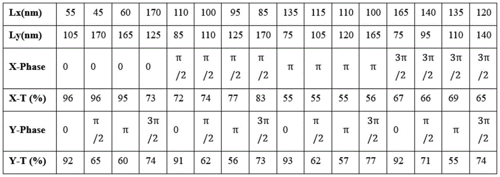
下列表1提供了各组相位值所对应的Lx和Ly值。其中,X-T和Y-T分别表示平行于x轴方向的线偏振光和平行于y轴方向的线偏振光的透过效率,X-phase和Y-phase分别表示x轴方向和y轴方向的相位值。由表1可知,优化后的硅纳米砖单元,在保证相位值的同时,还获得了较高的透过率和一致性。Table 1 below provides the corresponding Lx and Ly values for each set of phase values. Among them, XT and YT represent the transmission efficiency of the linearly polarized light parallel to the x-axis direction and the linearly polarized light parallel to the y-axis direction, respectively, and X-phase and Y-phase represent the phase values in the x-axis direction and the y-axis direction, respectively. . It can be seen from Table 1 that the optimized silicon nanobrick unit can obtain high transmittance and consistency while ensuring the phase value.
表1 Lx和Ly对应的4台阶位相值及透过效率对应表Table 1 Corresponding table of 4-step phase value and transmission efficiency corresponding to Lx and Ly
第四步:基于以下相位分布计算公式,得到纳米砖阵列上任意点的相位值,然后把连续相位进行4台阶量化,然后基于第三步的优化结果获取各相位对应的结构参数,把各单元结构排布到相应位置即得到如图3所示的超表面阵列结构。Step 4: Based on the following phase distribution calculation formula, obtain the phase value of any point on the nano-brick array, then quantify the continuous phase in 4 steps, and then obtain the structural parameters corresponding to each phase based on the optimization results of the third step, and quantify each cell. When the structures are arranged in corresponding positions, the metasurface array structure shown in Fig. 3 is obtained.


式中f为焦距,x,y为纳米砖在超表面阵列上的坐标。θx,θy为平行于x轴的线偏光和平行于y轴的线偏光经过纳米砖阵列后焦点离轴角度。λ为波长。where f is the focal length, and x and y are the coordinates of the nanobricks on the metasurface array. θ x , θ y are the off-axis angles of the focus after the linearly polarized light parallel to the x-axis and the linearly polarized light parallel to the y-axis pass through the nanobrick array. λ is the wavelength.
如图4所示,本实施例提供的智能光功率分配器件10的工作原理为:当沿着x方向的线偏光入射时,智能光功率分配器件10的分光比为1:0,当沿着y方向的线偏光入射时,智能光功率分配器件10的分光比为0:1。由于任意偏振态的光都能分解成两个相互正交线偏振光的组合。所以通过调整起偏器的旋转方向,能对任意偏振态的光实现的任意分光比M:N。As shown in FIG. 4 , the working principle of the intelligent optical
以上实施例仅仅是对本发明技术方案所做的举例说明。本发明所涉及的基于超表面材料的智能光功率分配器件并不仅仅限定于在以上实施例中所描述的内容,而是以权利要求所限定的范围为准。本发明所属领域技术人员在该实施例的基础上所做的任何修改或补充或等效替换,都在本发明的权利要求所要求保护的范围内。The above embodiments are merely examples to illustrate the technical solutions of the present invention. The metasurface material-based intelligent optical power distribution device involved in the present invention is not limited only to the content described in the above embodiments, but is subject to the scope defined by the claims. Any modifications or additions or equivalent substitutions made by those skilled in the art of the present invention on the basis of this embodiment are within the scope of protection claimed in the claims of the present invention.
Claims (2)


Priority Applications (1)
| Application Number | Priority Date | Filing Date | Title |
|---|---|---|---|
| CN201811037248.XA CN109164536B (en) | 2018-09-06 | 2018-09-06 | Intelligent optical power distribution device based on super surface material |
Applications Claiming Priority (1)
| Application Number | Priority Date | Filing Date | Title |
|---|---|---|---|
| CN201811037248.XA CN109164536B (en) | 2018-09-06 | 2018-09-06 | Intelligent optical power distribution device based on super surface material |
Publications (2)
| Publication Number | Publication Date |
|---|---|
| CN109164536A CN109164536A (en) | 2019-01-08 |
| CN109164536B true CN109164536B (en) | 2020-08-07 |
Family
ID=64894306
Family Applications (1)
| Application Number | Title | Priority Date | Filing Date |
|---|---|---|---|
| CN201811037248.XA Expired - Fee Related CN109164536B (en) | 2018-09-06 | 2018-09-06 | Intelligent optical power distribution device based on super surface material |
Country Status (1)
| Country | Link |
|---|---|
| CN (1) | CN109164536B (en) |
Families Citing this family (5)
| Publication number | Priority date | Publication date | Assignee | Title |
|---|---|---|---|---|
| CN109782390B (en) * | 2019-03-08 | 2020-06-16 | 北京邮电大学 | Optical beam splitter based on non-periodic sub-wavelength grating and design method thereof |
| CN111025430B (en) * | 2019-11-11 | 2021-05-18 | 武汉大学 | Metasurface Array Structure and Its Application in Image Display Multiplexing with Adjustable Grayscale |
| CN110989088B (en) * | 2019-12-06 | 2020-08-25 | 武汉大学 | Multiplexing/demultiplexing device and method based on lens and super-surface lens |
| CN112213800B (en) * | 2020-11-04 | 2022-04-19 | 中航华东光电有限公司 | Phase control type light deflection device based on micro-nano structure |
| CN115941044A (en) * | 2022-11-30 | 2023-04-07 | 武汉邮电科学研究院有限公司 | A metasurface optical broadcaster and communication system based on optical fiber end face |
Citations (5)
| Publication number | Priority date | Publication date | Assignee | Title |
|---|---|---|---|---|
| CN104777545A (en) * | 2015-05-05 | 2015-07-15 | 武汉大学 | A silicon nanobrick array polarizing beam splitter |
| CN107664780A (en) * | 2017-10-11 | 2018-02-06 | 武汉大学 | Dielectric nano brick array structure and its application as high-reflecting film and high transmittance film |
| CN107870446A (en) * | 2017-10-25 | 2018-04-03 | 武汉大学 | A Method of Converting Evanescent Waves into Traveling Waves |
| WO2018071870A2 (en) * | 2016-10-14 | 2018-04-19 | President And Fellows Of Harvard College | High performance visible wavelength meta-axicons for generating bessel beams |
| CN108490509A (en) * | 2018-04-08 | 2018-09-04 | 武汉大学 | The super surfacing of dielectric geometric phase of low depth-to-width ratio and its structural optimization method |
Family Cites Families (1)
| Publication number | Priority date | Publication date | Assignee | Title |
|---|---|---|---|---|
| US11231544B2 (en) * | 2015-11-06 | 2022-01-25 | Magic Leap, Inc. | Metasurfaces for redirecting light and methods for fabricating |
-
2018
- 2018-09-06 CN CN201811037248.XA patent/CN109164536B/en not_active Expired - Fee Related
Patent Citations (5)
| Publication number | Priority date | Publication date | Assignee | Title |
|---|---|---|---|---|
| CN104777545A (en) * | 2015-05-05 | 2015-07-15 | 武汉大学 | A silicon nanobrick array polarizing beam splitter |
| WO2018071870A2 (en) * | 2016-10-14 | 2018-04-19 | President And Fellows Of Harvard College | High performance visible wavelength meta-axicons for generating bessel beams |
| CN107664780A (en) * | 2017-10-11 | 2018-02-06 | 武汉大学 | Dielectric nano brick array structure and its application as high-reflecting film and high transmittance film |
| CN107870446A (en) * | 2017-10-25 | 2018-04-03 | 武汉大学 | A Method of Converting Evanescent Waves into Traveling Waves |
| CN108490509A (en) * | 2018-04-08 | 2018-09-04 | 武汉大学 | The super surfacing of dielectric geometric phase of low depth-to-width ratio and its structural optimization method |
Non-Patent Citations (5)
| Title |
|---|
| Broadband Focusing Flat Mirrors Based on Plasmonic Gradient Metasurfaces;Anders Pors et al.;《Nano Letters》;20130228(第13期);第829-834页 * |
| Dielectric metasurface based high-efficiency polarization splitters;Zhongyi Guo et al.;《RSC Advances》;20170203;第7卷(第16期);第9873-9874页 * |
| High-Order Dielectric Metasurfaces for High-Efficiency Polarization Beam Splitters and Optical Vortex Generators;Zhongyi Guo et al.;《Nanoscale Research Letters》;20170829;第12卷;第1-8页 * |
| Zhongyi Guo et al..Dielectric metasurface based high-efficiency polarization splitters.《RSC Advances》.2017,第7卷(第16期),第9872-9879页. * |
| 基于超表面结构的等离子体偏振器件的研究;李荣真;《中国优秀硕士学位论文全文数据库 工程科技Ⅱ辑》;20170215(第02期);第15-16页 * |
Also Published As
| Publication number | Publication date |
|---|---|
| CN109164536A (en) | 2019-01-08 |
Similar Documents
| Publication | Publication Date | Title |
|---|---|---|
| CN109164536B (en) | Intelligent optical power distribution device based on super surface material | |
| Li et al. | Efficient polarization beam splitter based on all-dielectric metasurface in visible region | |
| CN111090148B (en) | A multi-core optical fiber multiplexing and demultiplexing device and method based on metasurface lens | |
| CN110333560B (en) | Broadband achromatic device based on medium super surface | |
| CN105629463B (en) | A kind of design method for the circularly polarized light separator for surpassing surface based on artificial micro-structure | |
| CN105549130B (en) | Two grades of zoom lens based on polarization state control | |
| CN109212741B (en) | Continuous zoom lens and optical system | |
| CN110391579B (en) | Medium super-surface for generating double terahertz special beams | |
| Wang et al. | Inverse-designed Jones matrix metasurfaces for high-performance meta-polarizers | |
| CN106772795A (en) | A kind of photonic crystals splitter structure of efficient multifrequency point 1 × 3 | |
| CN109073815A (en) | Optical element | |
| CN110082906A (en) | Optical phased array based on imperfect asymmetric AWG | |
| Cai et al. | Observation of polarization-maintaining near-field directionality | |
| CN108873165B (en) | Random polarization state synthesizer of double-core optical fiber based on super-structure surface integration | |
| CN113568076B (en) | Double-function superlens and optical rotation detection method | |
| Ke et al. | Photonic crystal broadband y-shaped 1× 2 beam splitter inversely designed by genetic algorithm | |
| CN102650713B (en) | Photonic crystal waveguide TM-polarization separator | |
| Wang et al. | Design and optimization of non-uniform 1× 5 PLC splitter using orthogonal experimental method | |
| Xiong et al. | Triple-layer array splitter for zeroth-order suppressing under normal incidence | |
| CN114035247A (en) | All-dielectric metasurface structures for generating two-dimensional Airy vortex beams | |
| CN108828787A (en) | A kind of big field angle achromatic waveplate of micro-nano structure | |
| CN104102016B (en) | Photonic crystal based polarizing beam splitter design method | |
| CN111722420B (en) | Super-surface-based optical spin angular momentum spatial mode converter | |
| CN105607274A (en) | P-polarization-light controllable splitting ratio polarization beam splitter and work method thereof | |
| Zhang et al. | Aberration-corrected beam scanning system based on cascaded metalens arrays |
Legal Events
| Date | Code | Title | Description |
|---|---|---|---|
| PB01 | Publication | ||
| PB01 | Publication | ||
| SE01 | Entry into force of request for substantive examination | ||
| SE01 | Entry into force of request for substantive examination | ||
| GR01 | Patent grant | ||
| GR01 | Patent grant | ||
| CF01 | Termination of patent right due to non-payment of annual fee |
Granted publication date: 20200807 Termination date: 20210906 |
|
| CF01 | Termination of patent right due to non-payment of annual fee |